Low Power SRAM VLSI Final Presentation Stephen Durant






- Slides: 24

Low Power SRAM VLSI Final Presentation Stephen Durant Ryan Kruba Matt Restivo Voravit Vorapitat

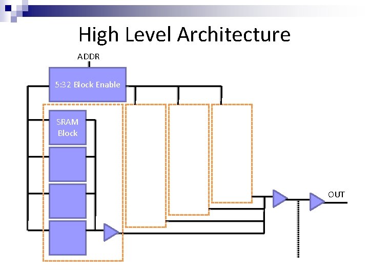
High Level Architecture ADDR 5: 32 Block Enable SRAM Block OUT

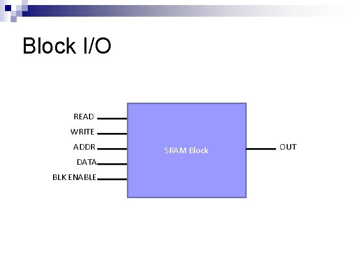
Block I/O READ WRITE ADDR DATA BLK ENABLE SRAM Block OUT

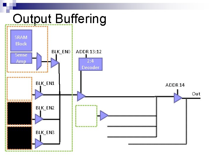
Output Buffering SRAM Block Sense Amp BLK_EN 0 ADDR 13: 12 2: 4 Decoder BLK_EN 1 ADDR 14 Out BLK_EN 2 BLK_EN 3

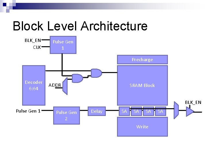
Block Level Architecture BLK_EN CLK Pulse Gen 1 Precharge Decoder 6: 64 ADDR SRAM Block BLK_EN Pulse Gen 1 Pulse Gen 2 Delay SA SA SA Write SA

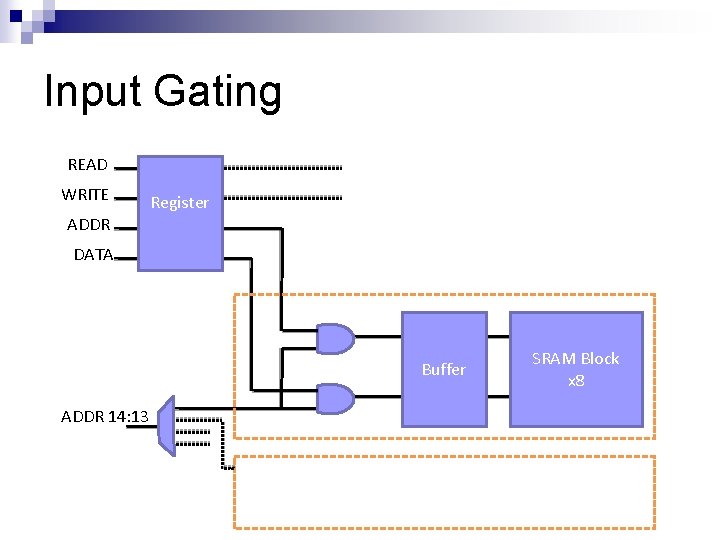
Input Gating READ WRITE Register ADDR DATA Buffer ADDR 14: 13 SRAM Block x 8

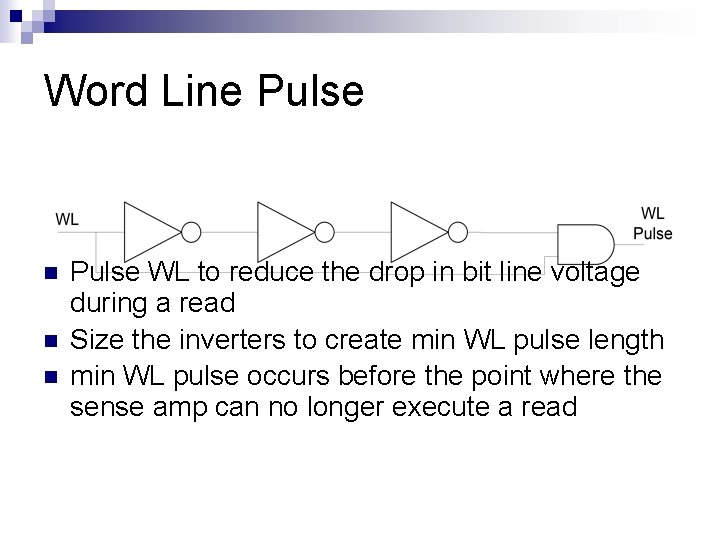
Word Line Pulse n n n Pulse WL to reduce the drop in bit line voltage during a read Size the inverters to create min WL pulse length min WL pulse occurs before the point where the sense amp can no longer execute a read

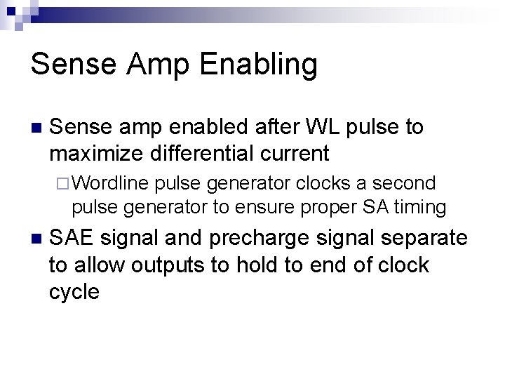
Sense Amp Enabling n Sense amp enabled after WL pulse to maximize differential current ¨ Wordline pulse generator clocks a second pulse generator to ensure proper SA timing n SAE signal and precharge signal separate to allow outputs to hold to end of clock cycle

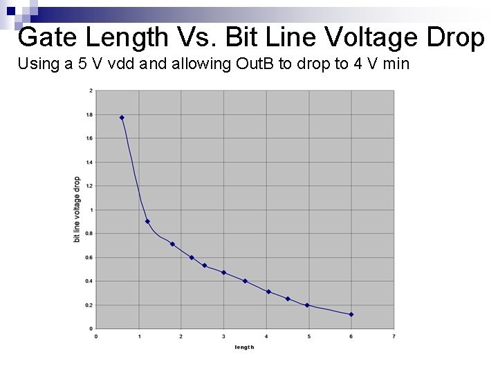
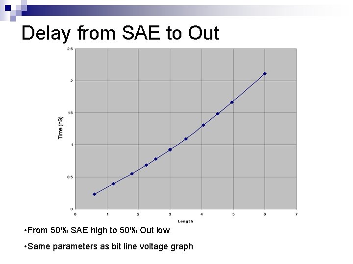
Sense Amp n Size three nmos transistors to control: ¨ Bit line voltage drop ¨ Delay

Gate Length Vs. Bit Line Voltage Drop Using a 5 V vdd and allowing Out. B to drop to 4 V min

Delay from SAE to Out • From 50% SAE high to 50% Out low • Same parameters as bit line voltage graph

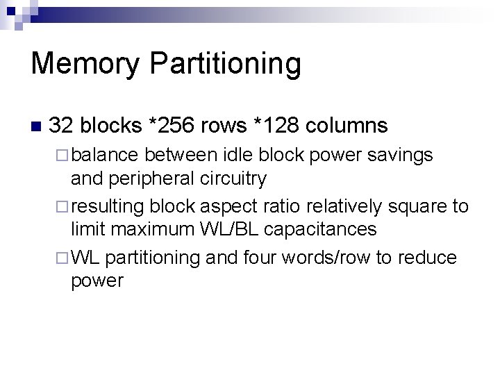
Memory Partitioning n 32 blocks *256 rows *128 columns ¨ balance between idle block power savings and peripheral circuitry ¨ resulting block aspect ratio relatively square to limit maximum WL/BL capacitances ¨ WL partitioning and four words/row to reduce power

Simulation Model n Multiple voltage sources to accurately measure energy ¨ Wordline, active column, inactive column, and peripheral n Etotal = EWL+32 Eact+96 Einact+E peripheral

Low Power Techniques

Optimal Signal Order for Energy Goal: Making WL pulse as short as possible. Read n SAE must be asserted only after WL pulse ends. Write n WL pulse must start after BL or BLB completely discharged.

Write ’ 0’ CLK BL WL SAE Read Write ’ 1’ Read

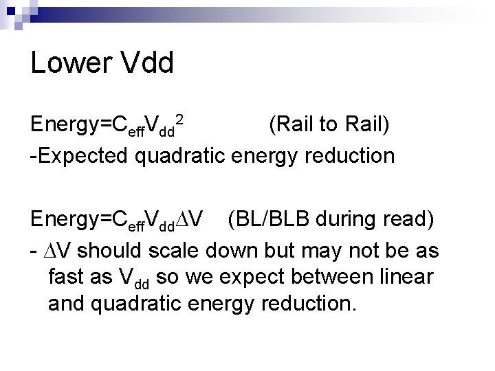
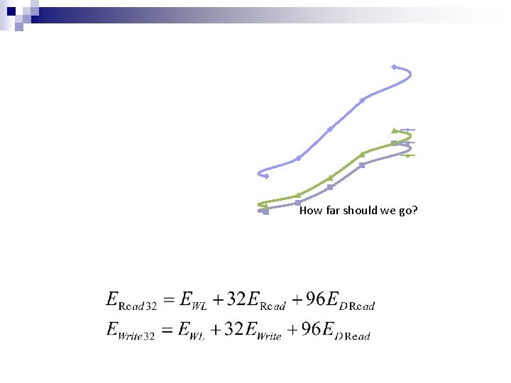
Lower Vdd Energy=Ceff. Vdd 2 (Rail to Rail) -Expected quadratic energy reduction Energy=Ceff. Vdd∆V (BL/BLB during read) - ∆V should scale down but may not be as fast as Vdd so we expect between linear and quadratic energy reduction.

Simulation Result for 1 bit 6 Energy vs Vdd for 1 bit read/write 5 Energy (p. J) 4 WL 3 Write Read DRead 2 1 0 0 0, 5 1 1, 5 Vdd (V) 2 2, 5 Note: The Read/Write/Dread shown here is BL energy only 3

250 Energy vs Vdd for 32 bit read/write Energy (p. J) 200 150 Total. Write Total. Read 100 Total Average 50 How far should we go? 0 0 0, 5 1 1, 5 Vdd (V) 2 2, 5 3

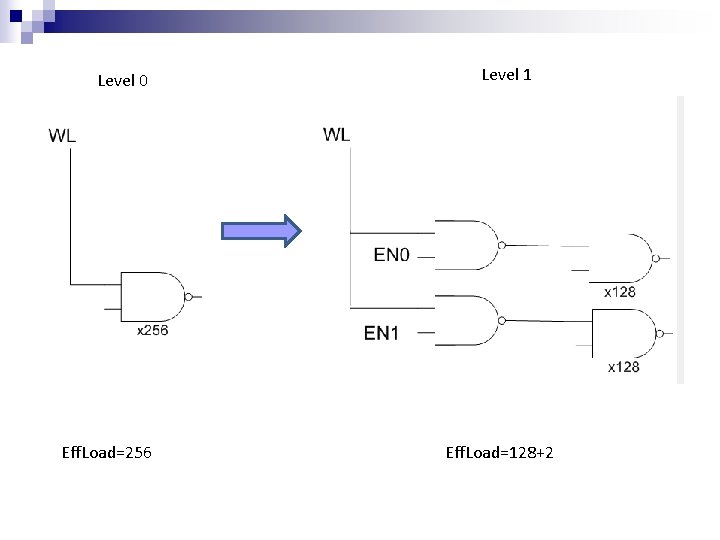
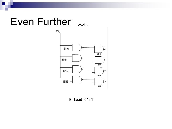
Clock Gating Try to reduce the capacitance that high activity signal have to drive. n Example: WL Pulse which have to drive 256 of 2 -input NAND! n

Level 0 Eff. Load=256 Level 1 Eff. Load=128+2

Even Further Level 2 Eff. Load=64+4

Simulation Result 25 Energy vs Clock Gating Level Energy (p. J) 20 15 10 5 0 0 0, 5 1 1, 5 2 Level of Clock Gating 2, 5 3 3, 5

Some note about clock gating n It act like a decoder, in our design we choose to use level 2 clock gating for WL pulse so we did not need 8 to 256 decode any more, we just need the 6 to 64.