Low Power Design of Standard Cell Digital VLSI









- Slides: 40

Low Power Design of Standard Cell Digital VLSI Circuits By Siri Uppalapati Thesis Directors: Prof. M. L. Bushnell and Prof. V. D. Agrawal ECE Department, Rutgers University May 18, 2004 MS Defense: Uppalapati 1

Talk Outline l l l Motivation Background Prior Work Proposed Design Flow Results Conclusion and Future Work May 18, 2004 MS Defense: Uppalapati 2

Motivation l Increasing gate count + increasing clock frequency = increasing POWER l Portable equipment runs on battery l Power consumption due to glitches can be 30 – 70% May 18, 2004 MS Defense: Uppalapati 3

Motivation: Chip Power Density Source: Intel Sun’s Surface Power Density (W/cm 2) 10000 Rocket Nozzle 1000 Nuclear Reactor 100 8086 Hot Plate 10 4004 8008 8085 386 286 8080 1 1970 May 18, 2004 1980 P 6 Pentium® 486 1990 Year 2000 MS Defense: Uppalapati 2010 4

Motivation (cont’d…) l Present day Application Specific Integrated Circuit (ASIC) chips employ standard cell based design style • A quick way to design circuits with millions of gates l Existing glitch reduction techniques demand gate re-design: not suitable for a cell-based design May 18, 2004 MS Defense: Uppalapati 5

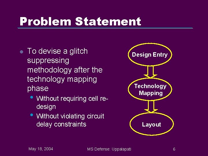
Problem Statement l To devise a glitch suppressing methodology after the technology mapping phase • Without requiring cell re • design Without violating circuit delay constraints May 18, 2004 MS Defense: Uppalapati Design Entry Technology Mapping Layout 6

Talk Progress l l l Motivation Background Prior Work Proposed Design Flow Results Conclusion and Future Work May 18, 2004 MS Defense: Uppalapati 7

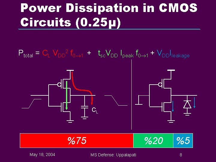
Power Dissipation in CMOS Circuits (0. 25µ) Ptotal = CL VDD 2 f 0 1 + tsc. VDD Ipeak f 0 1 + VDDIleakage CL %75 May 18, 2004 %20 MS Defense: Uppalapati %5 8

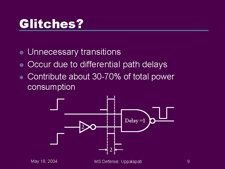
Glitches? l l l Unnecessary transitions Occur due to differential path delays Contribute about 30 -70% of total power consumption Delay =1 2 2 May 18, 2004 MS Defense: Uppalapati 9

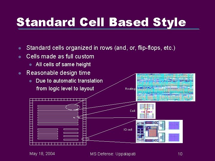
Standard Cell Based Style l l Standard cells organized in rows (and, or, flip-flops, etc. ) Cells made as full custom l l All cells of same height Reasonable design time l Due to automatic translation from logic level to layout Routing Cell IO cell May 18, 2004 MS Defense: Uppalapati 10

Talk Progress l l l Motivation Background Prior Work Proposed Design Flow Results Conclusion and Future Work May 18, 2004 MS Defense: Uppalapati 11

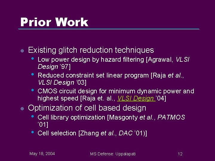
Prior Work l Existing glitch reduction techniques • • • l Low power design by hazard filtering [Agrawal, VLSI Design ’ 97] Reduced constraint set linear program [Raja et al. , VLSI Design ’ 03] CMOS circuit design for minimum dynamic power and highest speed [Raja et. al. , VLSI Design ’ 04] Optimization of cell based design • • Cell library optimization [Masgonty et al. , PATMOS ’ 01] Cell selection [Zhang et al. , DAC ’ 01)] May 18, 2004 MS Defense: Uppalapati 12

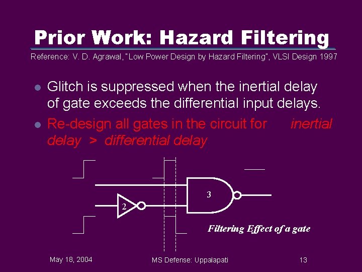
Prior Work: Hazard Filtering Reference: V. D. Agrawal, “Low Power Design by Hazard Filtering”, VLSI Design 1997 l l Glitch is suppressed when the inertial delay of gate exceeds the differential input delays. Re-design all gates in the circuit for inertial delay > differential delay 3 2 Filtering Effect of a gate May 18, 2004 MS Defense: Uppalapati 13

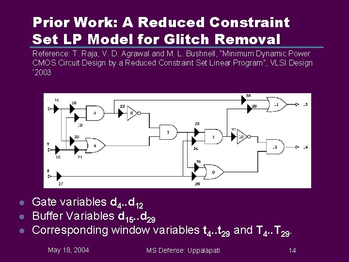
Prior Work: A Reduced Constraint Set LP Model for Glitch Removal Reference: T. Raja, V. D. Agrawal and M. L. Bushnell, “Minimum Dynamic Power CMOS Circuit Design by a Reduced Constraint Set Linear Program”, VLSI Design ‘ 2003 l l l Gate variables d 4. . d 12 Buffer Variables d 15. . d 29 Corresponding window variables t 4. . t 29 and T 4. . T 29. May 18, 2004 MS Defense: Uppalapati 14

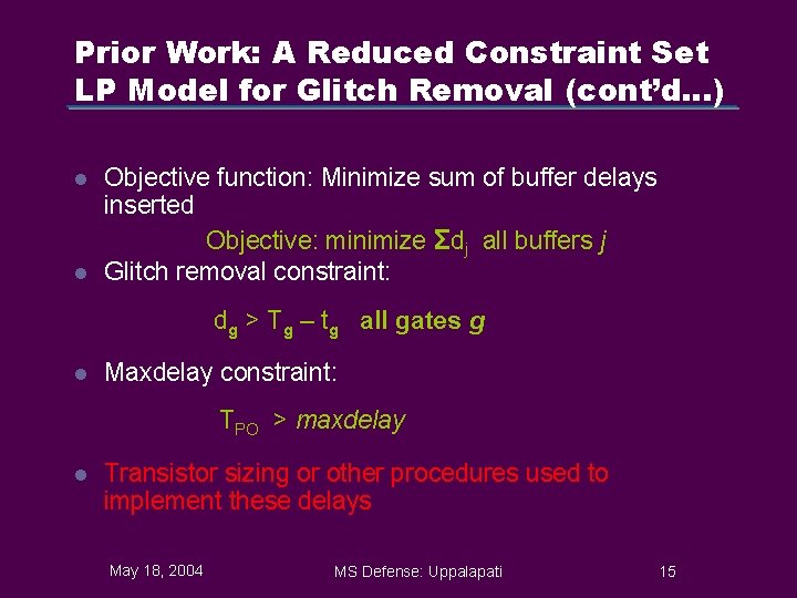
Prior Work: A Reduced Constraint Set LP Model for Glitch Removal (cont’d…) l l Objective function: Minimize sum of buffer delays inserted Objective: minimize Σdj all buffers j Glitch removal constraint: dg > Tg – tg all gates g l Maxdelay constraint: TPO > maxdelay l Transistor sizing or other procedures used to implement these delays May 18, 2004 MS Defense: Uppalapati 15

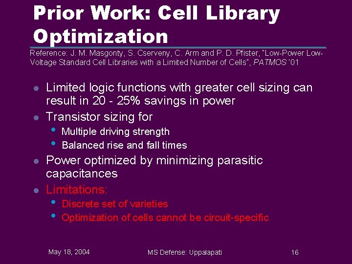
Prior Work: Cell Library Optimization Reference: J. M. Masgonty, S. Cserveny, C. Arm and P. D. Pfister, “Low-Power Low. Voltage Standard Cell Libraries with a Limited Number of Cells”, PATMOS ‘ 01 l l Limited logic functions with greater cell sizing can result in 20 - 25% savings in power Transistor sizing for • • Multiple driving strength Balanced rise and fall times Power optimized by minimizing parasitic capacitances Limitations: • • Discrete set of varieties Optimization of cells cannot be circuit-specific May 18, 2004 MS Defense: Uppalapati 16

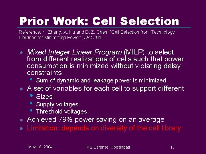
Prior Work: Cell Selection Reference: Y. Zhang, X. Hu and D. Z. Chen, “Cell Selection from Technology Libraries for Minimizing Power”, DAC ‘ 01 l l Mixed Integer Linear Program (MILP) to select from different realizations of cells such that power consumption is minimized without violating delay constraints • Sum of dynamic and leakage power is minimized • • Supply voltages Threshold voltages A set of variables for each cell to support different • Sizes Achieved 79% power saving on an average Limitation: depends on diversity of the cell library May 18, 2004 MS Defense: Uppalapati 17

Talk Progress l l l Motivation Background Prior Work Proposed Design Flow Results Conclusion and Future Work May 18, 2004 MS Defense: Uppalapati 18

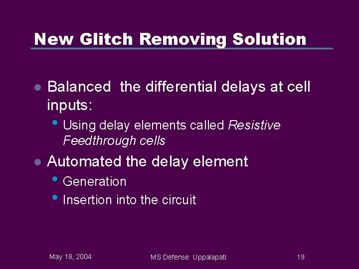
New Glitch Removing Solution l Balanced the differential delays at cell inputs: • Using delay elements called Resistive Feedthrough cells l Automated the delay element • Generation • Insertion into the circuit May 18, 2004 MS Defense: Uppalapati 19

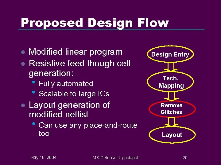
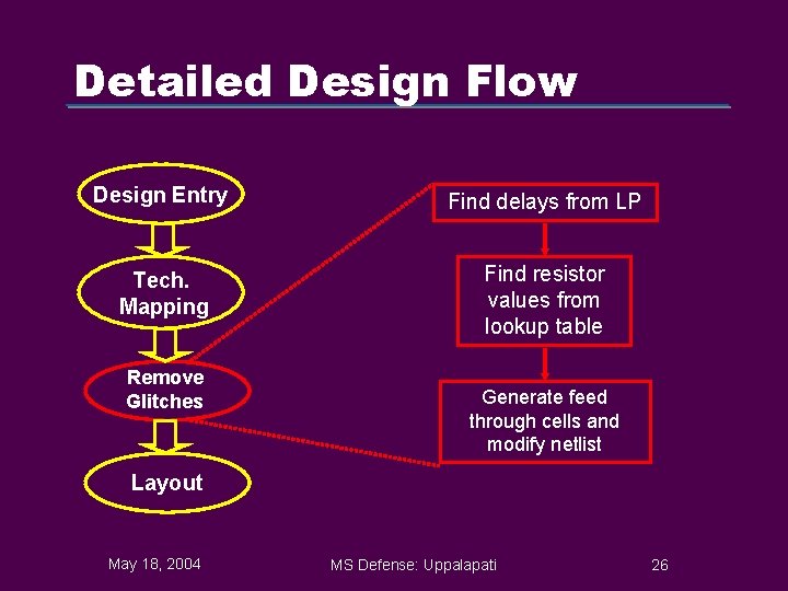
Proposed Design Flow l l l Modified linear program Resistive feed though cell generation: Design Entry • Fully automated • Scalable to large ICs Tech. Mapping Layout generation of modified netlist Remove Glitches • Can use any place-and-route tool May 18, 2004 Layout MS Defense: Uppalapati 20

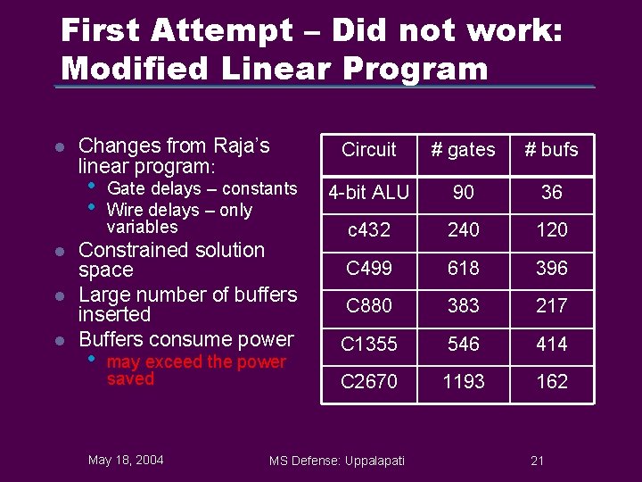
First Attempt – Did not work: Modified Linear Program l Changes from Raja’s linear program: • • l l l Gate delays – constants Wire delays – only variables Constrained solution space Large number of buffers inserted Buffers consume power • may exceed the power saved May 18, 2004 Circuit # gates # bufs 4 -bit ALU 90 36 c 432 240 120 C 499 618 396 C 880 383 217 C 1355 546 414 C 2670 1193 162 MS Defense: Uppalapati 21

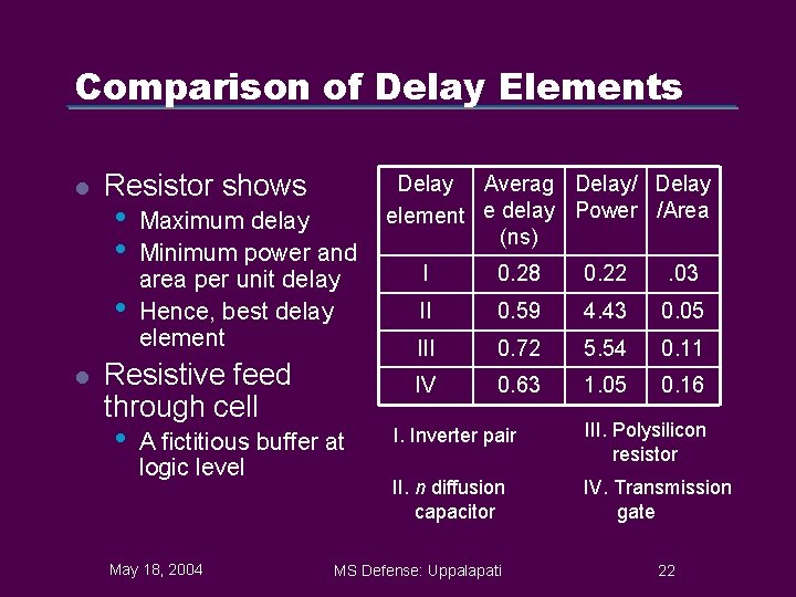
Comparison of Delay Elements l Resistor shows • • • l Maximum delay Minimum power and area per unit delay Hence, best delay element Resistive feed through cell • A fictitious buffer at logic level May 18, 2004 Delay Averag Delay/ Delay element e delay Power /Area (ns) I 0. 28 0. 22 . 03 II 0. 59 4. 43 0. 05 III 0. 72 5. 54 0. 11 IV 0. 63 1. 05 0. 16 I. Inverter pair III. Polysilicon resistor II. n diffusion capacitor IV. Transmission gate MS Defense: Uppalapati 22

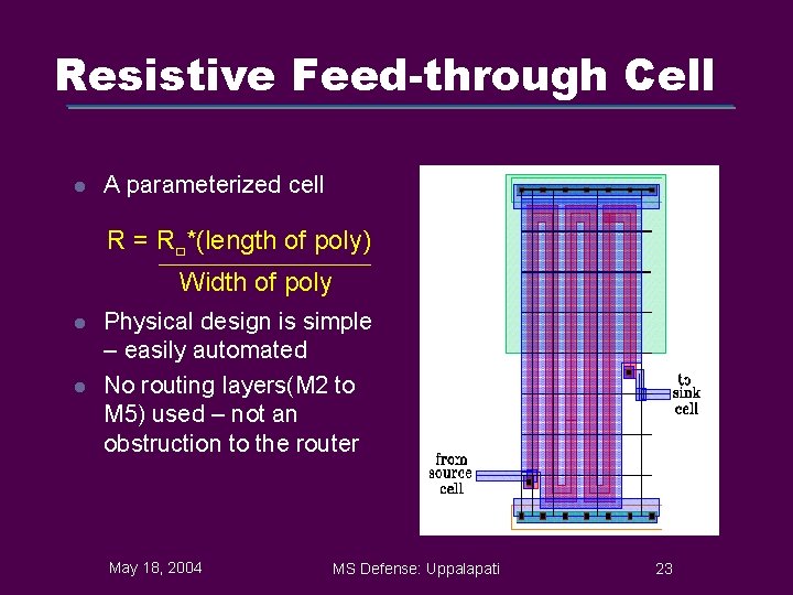
Resistive Feed-through Cell l A parameterized cell R = R□*(length of poly) Width of poly l l Physical design is simple – easily automated No routing layers(M 2 to M 5) used – not an obstruction to the router May 18, 2004 MS Defense: Uppalapati 23

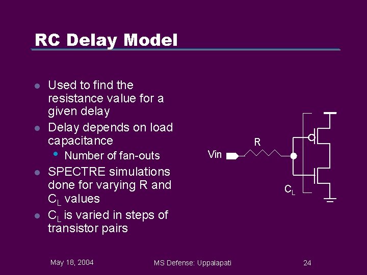
RC Delay Model l l Used to find the resistance value for a given delay Delay depends on load capacitance • l l Number of fan-outs R Vin SPECTRE simulations done for varying R and CL values CL is varied in steps of transistor pairs May 18, 2004 MS Defense: Uppalapati CL 24

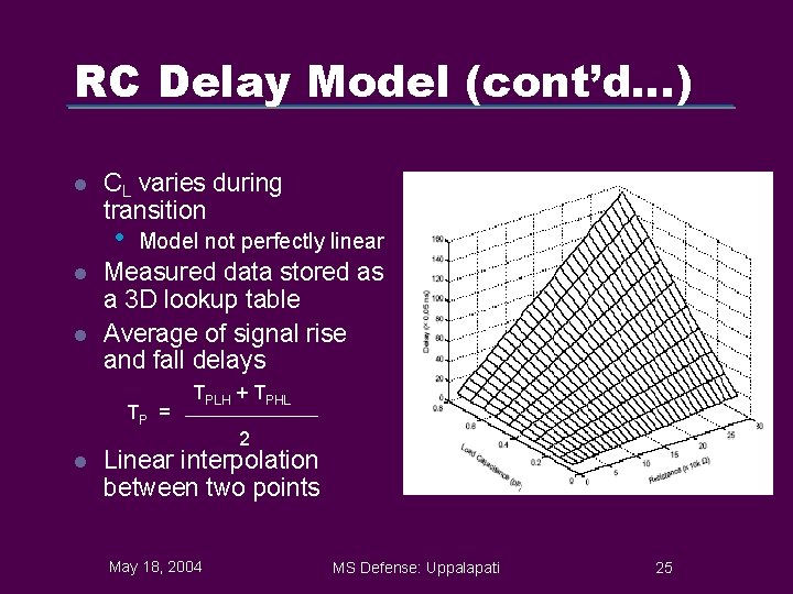
RC Delay Model (cont’d…) l CL varies during transition • l l Model not perfectly linear Measured data stored as a 3 D lookup table Average of signal rise and fall delays TP = TPLH + TPHL 2 l Linear interpolation between two points May 18, 2004 MS Defense: Uppalapati 25

Detailed Design Flow Design Entry Find delays from LP Tech. Mapping Find resistor values from lookup table Remove Glitches Generate feed through cells and modify netlist Layout May 18, 2004 MS Defense: Uppalapati 26

Talk Progress l l l Motivation Background Prior Work Proposed Design Flow Results Conclusion and Future Work May 18, 2004 MS Defense: Uppalapati 27

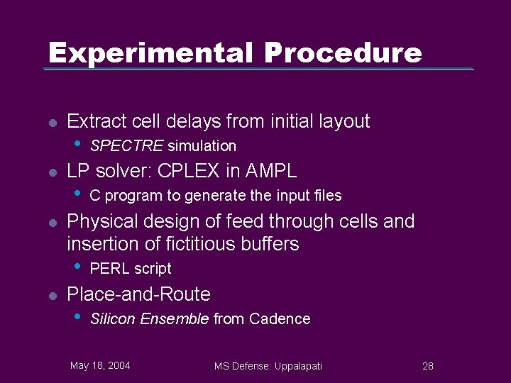
Experimental Procedure l l l Extract cell delays from initial layout • LP solver: CPLEX in AMPL • C program to generate the input files Physical design of feed through cells and insertion of fictitious buffers • l SPECTRE simulation PERL script Place-and-Route • Silicon Ensemble from Cadence May 18, 2004 MS Defense: Uppalapati 28

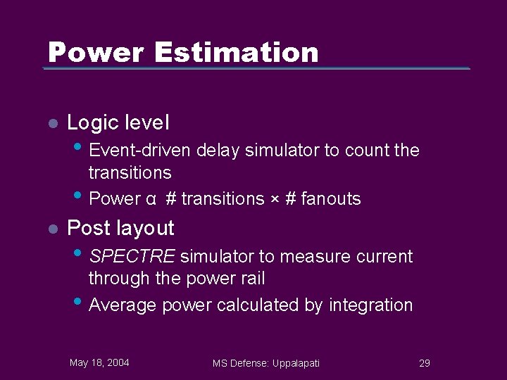
Power Estimation l Logic level • Event-driven delay simulator to count the • l transitions Power α # transitions × # fanouts Post layout • SPECTRE simulator to measure current • through the power rail Average power calculated by integration May 18, 2004 MS Defense: Uppalapati 29

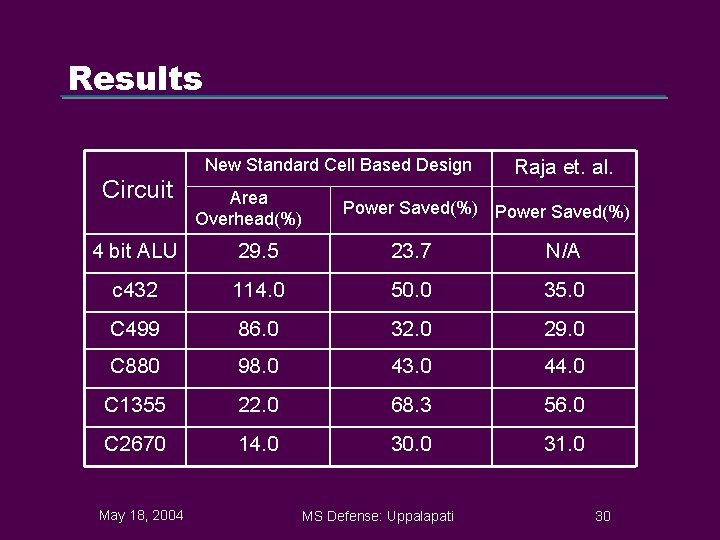
Results New Standard Cell Based Design Circuit Area Overhead(%) Raja et. al. Power Saved(%) 4 bit ALU 29. 5 23. 7 N/A c 432 114. 0 50. 0 35. 0 C 499 86. 0 32. 0 29. 0 C 880 98. 0 43. 0 44. 0 C 1355 22. 0 68. 3 56. 0 C 2670 14. 0 30. 0 31. 0 May 18, 2004 MS Defense: Uppalapati 30

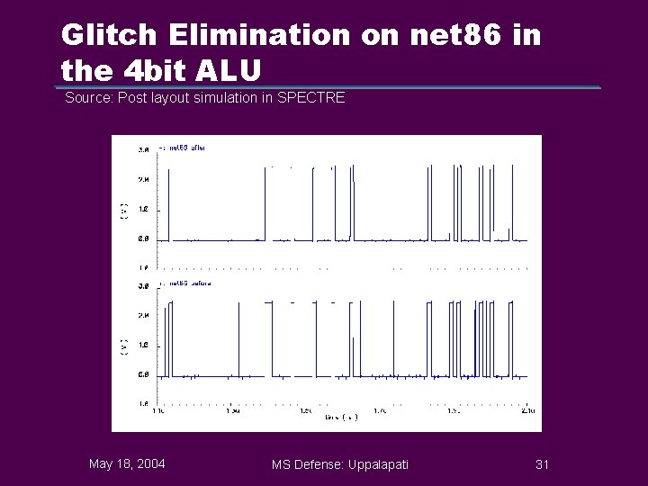
Glitch Elimination on net 86 in the 4 bit ALU Source: Post layout simulation in SPECTRE May 18, 2004 MS Defense: Uppalapati 31

Energy Saving in 4 bit ALU May 18, 2004 MS Defense: Uppalapati 32

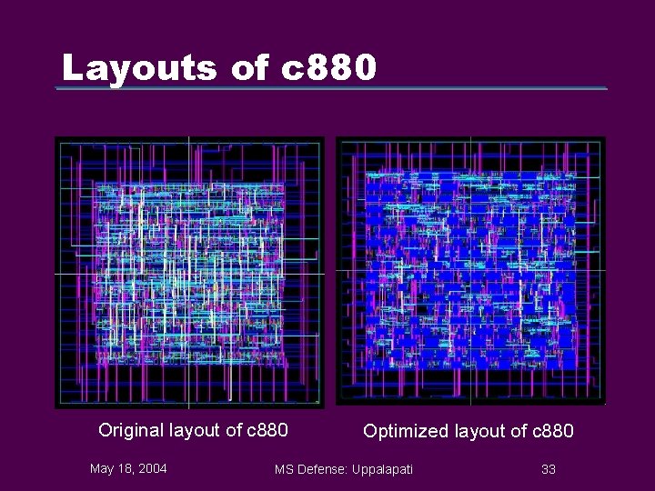
Layouts of c 880 Original layout of c 880 May 18, 2004 Optimized layout of c 880 MS Defense: Uppalapati 33

Talk Progress l l l Motivation Background Prior Work Proposed Design Flow Results Conclusion and Future Work May 18, 2004 MS Defense: Uppalapati 34

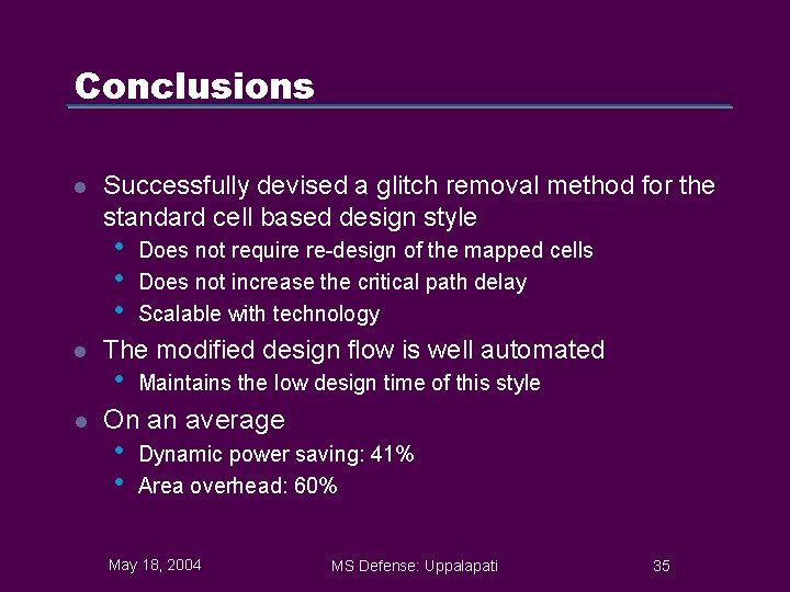
Conclusions l Successfully devised a glitch removal method for the standard cell based design style • • • l l Does not require re-design of the mapped cells Does not increase the critical path delay Scalable with technology The modified design flow is well automated • Maintains the low design time of this style On an average • • Dynamic power saving: 41% Area overhead: 60% May 18, 2004 MS Defense: Uppalapati 35

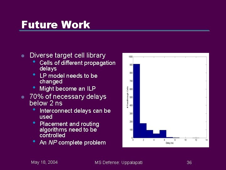
Future Work l l Diverse target cell library • • • Cells of different propagation delays LP model needs to be changed Might become an ILP • • Interconnect delays can be used Placement and routing algorithms need to be controlled An NP complete problem 70% of necessary delays below 2 ns • May 18, 2004 MS Defense: Uppalapati 36

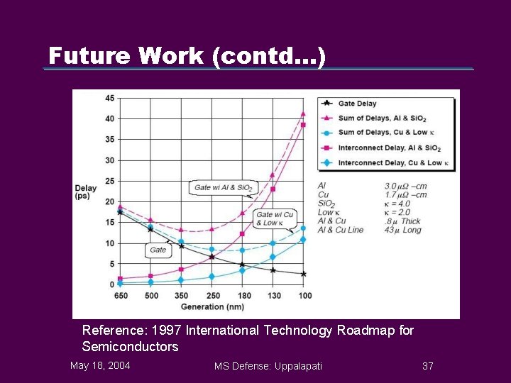
Future Work (contd…) Reference: 1997 International Technology Roadmap for Semiconductors May 18, 2004 MS Defense: Uppalapati 37

References l l V. D. Agrawal, “Low Power Design by Hazard Filtering”, VLSI Design 1997 T. Raja, V. D. Agrawal and M. L. Bushnell, “Minimum Dynamic Power CMOS Circuit Design by a Reduced Constraint Set Linear Program”, VLSI Design 2003 Y. Zhang, X. Hu and D. Z. Chen, “Cell Selection from Technology Libraries for Minimizing Power”, DAC 2001 J. M. Masgonty, S. Cserveny, C. Arm and P. D. Pfister, “Low-Power Low-Voltage Standard Cell Libraries with a Limited Number of Cells”, PATMOS 2001 May 18, 2004 MS Defense: Uppalapati 38

THANK YOU May 18, 2004 MS Defense: Uppalapati 39

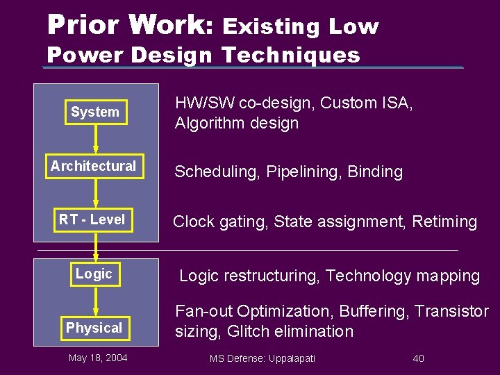
Prior Work: Existing Low Power Design Techniques System Architectural RT - Level HW/SW co-design, Custom ISA, Algorithm design Scheduling, Pipelining, Binding Clock gating, State assignment, Retiming Logic restructuring, Technology mapping Physical Fan-out Optimization, Buffering, Transistor sizing, Glitch elimination May 18, 2004 MS Defense: Uppalapati 40