Logic Synthesis Tutorial Pusan National University Introduction A
- Slides: 10

Logic Synthesis Tutorial Pusan National University

Introduction • A new way for logic design – HDL(Hardware Description Language)-based design method – This is what we are studying in this course – First, hierarchical RTL structure and corresponding behavior are thought, and described in HDL by designers – Then, all Boolean logic equations are generated automatically by logic synthesis – Corresponding schematic are also generated automatically by logic synthesis – Much less error-prone, and tedious

Introduction • History of Logic Synthesis – Pioneered by some researchers at IBM and UC Berkeley in 1980’s – Commercialized by Synopsys, the biggest EDA company – Revolutionized the way of logic design • From error-prone manual logic design to error-free automatic logic design

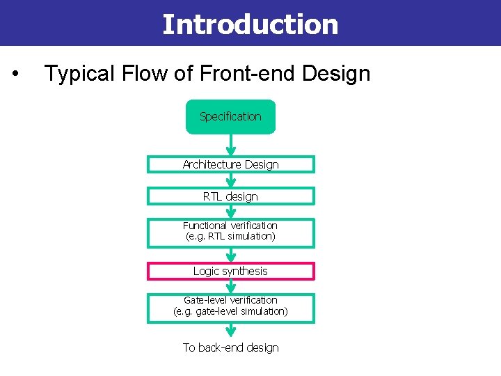
Introduction • Typical Flow of Front-end Design Specification Architecture Design RTL design Functional verification (e. g. RTL simulation) Logic synthesis Gate-level verification (e. g. gate-level simulation) To back-end design

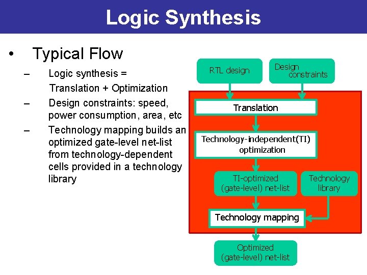
Logic Synthesis • Typical Flow – – – Logic synthesis = Translation + Optimization Design constraints: speed, power consumption, area, etc Technology mapping builds an optimized gate-level net-list from technology-dependent cells provided in a technology library RTL design Design constraints Translation Technology-independent(TI) optimization TI-optimized (gate-level) net-list Technology mapping Optimized (gate-level) net-list Technology library

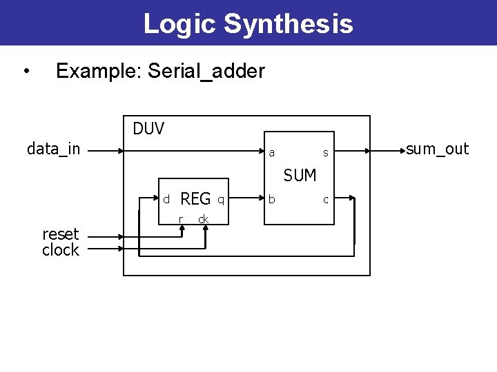
Logic Synthesis • Example: Serial_adder data_in DUV a s SUM d reset clock REG r ck q b c sum_out

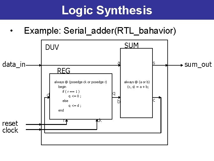
Logic Synthesis • Example: Serial_adder(RTL_bahavior) SUM DUV data_in a REG d reset clock s always @ (posedge ck or posedge r) begin if ( r == 1 ) q <= 0 ; else q <= d ; end r ck always @ (a or b) {c, s} = a + b; q b c sum_out

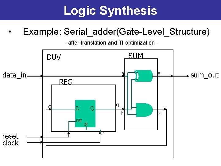
Logic Synthesis • Example: Serial_adder(Gate-Level_Structure) - after translation and TI-optimization - SUM DUV data_in s b c REG d D rst reset clock a r q Q ck ck sum_out

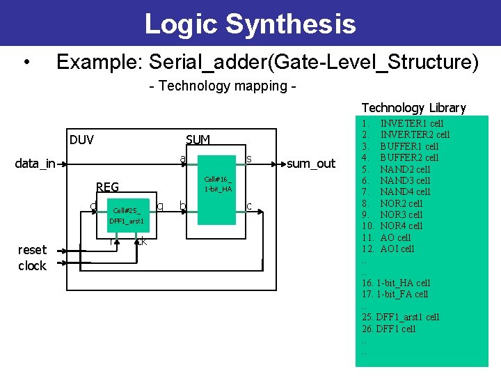
Logic Synthesis • Example: Serial_adder(Gate-Level_Structure) - Technology mapping Technology Library DUV SUM a data_in Cell#16_ 1 -bit_HA REG d reset clock Cell#25_ DFF 1_arst 1 r s ck q b c sum_out 1. INVETER 1 cell 2. INVERTER 2 cell 3. BUFFER 1 cell 4. BUFFER 2 cell 5. NAND 2 cell 6. NAND 3 cell 7. NAND 4 cell 8. NOR 2 cell 9. NOR 3 cell 10. NOR 4 cell 11. AO cell 12. AOI cell. . 16. 1 -bit_HA cell 17. 1 -bit_FA cell. . 25. DFF 1_arst 1 cell 26. DFF 1 cell. .

Assignment • Logic Synthesis Lab. – – Complete your RTL design, write a test bench, and perform RTL simulation With your example RTL design and Xilinx ISE, perform the entire logic synthesis process to obtain a technology dependent gate-level netlist At each step in the logic synthesis process with Xilinx ISE, take a screen shot and identify to where it belongs in the typical flow of logic synthesis You should obtain a gate-level Verilog structural code as the final result, and make a PPT file for a possible presentation including the RTL simulation result