Logic Synthesis Sequential Synthesis Courtesy RK Brayton UCB
Logic Synthesis Sequential Synthesis Courtesy RK Brayton (UCB) and A Kuehlmann (Cadence) 1

Introduction • Design optimization from System level to layout – far too complex to approach in one big step – Þ divide and conquer approach with fine tuned balance between • capability to apply clean mathematical modeling and abstraction • algorithmic complexity to compute solutions • loss of optimality based on hard partitioning • design and verification methodology that requires user guidance – sweet spots change over time due to: • semi-conductor technology improvements • changes of design architectures/requirements • new algorithmic solutions, etc.
Introduction • Example: traditional ASIC methodology: – RTL verification based on simulation – logic synthesis from RTL to gate level using combinational paradigm – static timing analysis – formal equivalence checking based on combinational paradigm – ATPG and scan-based testing based on combinational paradigm – standard cell place & route methodology with zero clock-skew distribution

Introduction • However: – clean boundaries between modeling levels get blurred • larger chips and shrinking device sizes require more detailed modeling • aggressive performance and power requirements • new modeling and algorithmic approaches – Example: • RTL sign-off methodology • combined approach to logic synthesis and physical design 4

Combinational Optimization Clock Skew Scheduling Retiming Architectural Restructuring Verification Challenge Necessity of Integrated Solution Optimization Space Distance from Physical Implementation Overview of Circuit Optimizations System-Level Optimization 5

Sequential Optimization Techniques • State assignment – Lots of theory, practical only for small FSMs, that too targeting 2 -level control logic • Sequential don’t cares – Compute unreachable states, use them as external don’t cares for the next-state logic • State minimization – Easy for completely specified FSMs (n ¢ log n algorithm) – Incompletely specified FSMs • Retiming – balancing of path delays by moving registers within circuit topology – interleaving with combinational optimization techniques 6
Integration in Design Flow • Optimization Space – significant more optimization freedom for improving performance, power, and area • Distance from Physical Implementation – difficult to accurately model impact on final implementation – difficult to mathematically characterize optimization space • Verification Challenge – departure from combinational comparison model would break formal equivalence checking – different simulation behavior causes acceptance problems 7

Retiming r 3 r 2 4 5 2 r 1 3 4 5 2 Dmax=6 3 r’ 1 Dmin=0 Dmin=3 r’ 1 r 4 Dmax=0 Dmax=8 Dmin=2 r 4 Skew =0 Tcycle=8 = -1 ) ( Skew T =7 cycle 8
Retiming + - • Only setup time constraint (0 clock skew) • Simple integration with other logical (e. g. combinational) or physical optimizations • Easy combination with clock skew scheduling to obtain global optimum • Changes combinational model of design – severe impact on verification methodology • Inaccurate delay model if applied globally • Computation of equivalent reset state required 9

Retiming - Architectural Restructuring 2 r 2 2 20. . . { r 2 r 3 . . . 2 r 4 r 1 r 2 2 10 r’ 4 10 { { 2 r 3 . . . r’ 1 . . . 2 r 4 10
Retiming - Architectural Restructuring + - • Smooth extension of regular retiming • Potential to alleviate global performance bottlenecks by adding sequential redundancy and pipelining • Significant change of design structure – substantial impact on verification methodology • Flexible architectural restructuring changes I/O behavior – existing RTL specification methods not always applicable 11

Example Design example: - 360 I/O - 2240 flip-flops - 41665 timing edges Target cycle time (norm): 1. 5 Worst slack: -0. 079 (5%) Distribution: 20% 30 edges 40% 63 edges 60% 130 edges 80% 249 edges 100% 425 edges 12

Verification • Timing verification unchanged • Sequential optimizations change the next-state and output functions – traditional combinational equivalence checking not applicable – simulation runs not recognizable by designer - acceptance problems • Generic solution: – preserve retime function (mapping function) from synthesis for: • reducing sequential EC problem back to combinational case – no false positives possible!!!! • modifying simulation model to reproduce original simulation output 13

Optimizing Circuits by Retiming Netlist of gates and registers: Inputs Outputs Various Goals: – Reduce clock cycle time – Reduce area • Reduce number of latches 14

Retiming Problem – Pure combinational optimization can be suboptimal since relations across register boundaries are disregarded Solutions – Retiming: Move register(s) so that • clock cycle decreases, or number of registers decreases and • input-output behavior is preserved – Rn. R: Combine retiming with combinational optimization techniques • Move latches out of the way temporarily • optimize larger blocks of combinational 15
![Circuit Representation [Leiserson, Rose and Saxe (1983)] Circuit represented as retiming graph G(V, E, Circuit Representation [Leiserson, Rose and Saxe (1983)] Circuit represented as retiming graph G(V, E,](http://slidetodoc.com/presentation_image_h/bd80d73bc2275bc2d9b096ac9469ecbb/image-16.jpg)
Circuit Representation [Leiserson, Rose and Saxe (1983)] Circuit represented as retiming graph G(V, E, d, w) – V set of gates – E set of connections – d(v) = delay of gate/vertex v, (d(v) 0) – w(e) = number of registers on edge e, (w(e) 0) 16

Circuit Representation Example: Correlator (from Leiserson and Saxe) (simplified) + 0 Host 0 (x, y) = 1 if x=y 0 otherwise 7 0 0 2 3 3 0 Retiming Graph (Directed) a b Circuit Every cycle in Graph has at least one register i. e. no combinational loops. Operation delay 3 + 7 17

Preliminaries For a path p : Clock cycle 0 0 7 Path with 0 0 2 3 0 w(p)=0 3 For correlator c = 13 18

Basic Operation • Movement of registers from input to output of a gate or vice versa Retime by -1 Retime by 1 • • Does not affect gate functionality's Mathematical formulation: – r: V Z, an integer vertex labeling – wr(e) = w(e) + r(v) - r(u) for edge e = (u, v) 19

Basic Operation Thus in the example, r(u) = -1, r(v) = -1 results in 0 0 0 2 • • 7 3 0 0 u 0 v 0 3 7 1 1 3 1 v u 0 3 For a path p: s t, wr(p) = w(p) + r(t) - r(s) Retiming: – r: V Z, an integer vertex labeling – wr(e) =w(e) + r(v) - r(u) for edge e= (u, v) – A retiming r is legal if wr(e) 0, e E 20
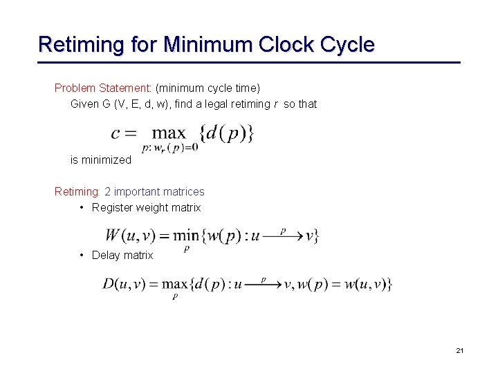
Retiming for Minimum Clock Cycle Problem Statement: (minimum cycle time) Given G (V, E, d, w), find a legal retiming r so that is minimized Retiming: 2 important matrices • Register weight matrix • Delay matrix 21

Retiming for minimum clock cycle 0 v 0 0 7 3 V 1 V 0 V 1 V 2 V 3 0 0 2 W = register path weight matrix (minimum # latches on all paths between u and v) D = path delay matrix (maximum delay on all paths between u and v) 0 3 V 2 W D V 0 V 1 V 2 V 3 0222 0000 0220 0 3 6 13 3 6 10 13 3 7 10 13 13 13 10 7 V 0 V 1 V 2 V 3 c p, if d(p) then w(p) 1 22

Conditions for Retiming Assume that we are asked to check if a retiming exists for a clock cycle Legal retiming: wr(e) 0 for all e. Hence wr(e) = w(e) = r(v) - r(u) 0 or r (u) - r (v) w (e) For all paths p: u v such that d(p) , we require wr(p) 1 – Thus Take the least w(p) (tightest constraint) r(u)-r(v) W(u, v)-1 Note: this is independent of the path from u to v, so we just need to apply it to u, v such that D(u, v) 23
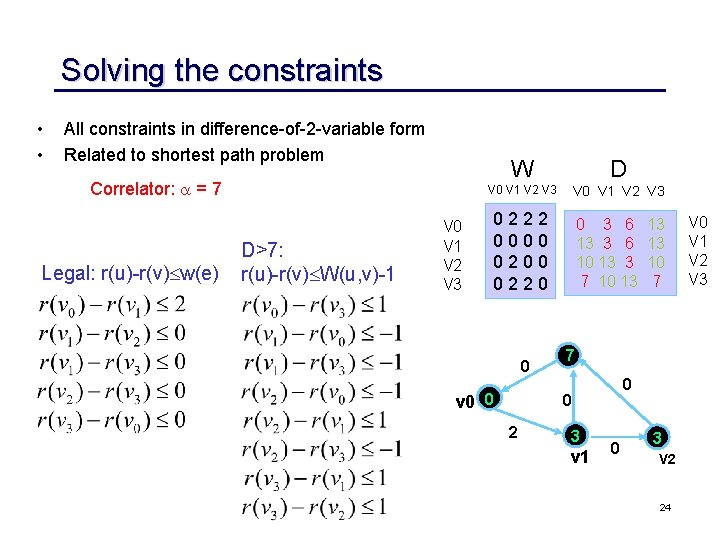
Solving the constraints • • All constraints in difference-of-2 -variable form Related to shortest path problem Correlator: = 7 Legal: r(u)-r(v) w(e) D>7: r(u)-r(v) W(u, v)-1 V 0 V 1 V 2 V 3 W D V 0 V 1 V 2 V 3 0222 0000 0220 0 v 0 0 0 3 6 13 3 6 10 13 3 7 10 13 7 0 0 2 13 13 10 7 3 v 1 0 3 V 2 24 V 0 V 1 V 2 V 3

Solving the constraints • • Do shortest path on constraint graph: (O(|V||E| )) (Bellman Ford Algorithm) A solution exists if and only if there exists no negative weighted cycle. Legal: r(u)-r(v) w(e) Constraint graph D>7: r(u)-r(v) W(u, v)-1 -1 0 r(0) 0 0 0 -1 -1 2 r(1) 1 1 0, -1 0 r(2) 0, -1 -1 A solution is r(v 0) = r(v 3) = 0, r(v 1) = r(v 2) = -1 r(3) 0 1 25

Retiming To find the minimum cycle time, do a binary search among the entries of the D matrix (0( V E log V )) 0 v 0 0 7 0 0 2 3 0 v 1 V 0 V 1 V 2 V 3 3 V 2 W D V 0 V 1 V 2 V 3 0222 0000 0220 Retimed correlator: + Retime Host 0 13 10 7 3 3 13 10 6 13 3 10 13 7 + Host Clock cycle = 3+3+7=13 Clock cycle = 7 a b 26 V 0 V 1 V 2 V 3

Retiming: 2 more algorithms 1. Relaxation based: – Repeatedly find critical path; – retime vertex at end of path by +1 (O( V E log V )) v +1 Critical path u 2. Also, Mixed Integer Linear Program formulation 27

Retiming for Minimum Area Goal: minimize number of registers used where av is a constant. 28

Minimum Registers - Formulation Minimize: Subject to: wr(e) =w(e) + r(v) - r(u) 0 • Reducible to a flow problem 29

Problems with Retiming • Computation of equivalent initial states – do not exist necessarily 1 0 ? ? – General solution requires replication of logic for initialization • Timing models – too far away from actual implementation 30
- Slides: 30