Logic synthesis flow Technology independent mapping Two level
- Slides: 11

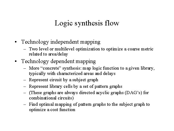
Logic synthesis flow • Technology independent mapping – Two level or multilevel optimization to optimize a coarse metric related to area/delay • Technology dependent mapping – More “concrete” synthesis: map logic function to a given library, typically with characterized areas and delays – Represent circuit by a subject graph – Represent library cells by a set of pattern graphs – (These graphs are always directed acyclic graphs (DAG’s) for combinational circuits) – Find optimal mapping of pattern graphs to the subject graph to optimize a cost function

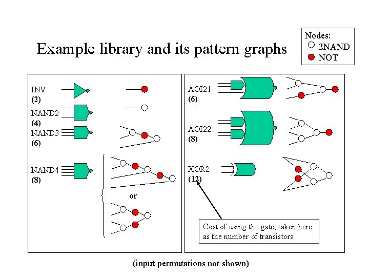
Example library and its pattern graphs Nodes: 2 NAND NOT AOI 21 (6) INV (2) NAND 2 (4) NAND 3 (6) AOI 22 (8) XOR 2 (12) NAND 4 (8) or Cost of using the gate, taken here as the number of transistors (input permutations not shown)

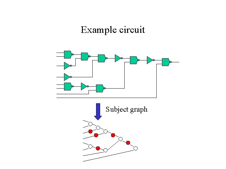
Example circuit Subject graph

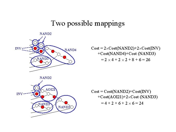
Two possible mappings NAND 2 INV NAND 4 NAND 3 Cost = 2 Cost(NAND 2)+2 Cost(INV) +Cost(NAND 4)+Cost (NAND 3) = 2 4 + 2 2 + 8 + 6 = 26 NAND 2 AOI 21 INV NAND 3 Cost = Cost(NAND 2)+Cost(INV) +Cost(AOI 21)+2 Cost (NAND 3) = 4 + 2 + 6 + 2 6 = 24

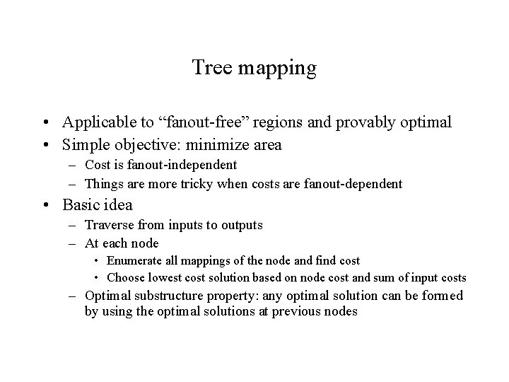
Tree mapping • Applicable to “fanout-free” regions and provably optimal • Simple objective: minimize area – Cost is fanout-independent – Things are more tricky when costs are fanout-dependent • Basic idea – Traverse from inputs to outputs – At each node • Enumerate all mappings of the node and find cost • Choose lowest cost solution based on node cost and sum of input costs – Optimal substructure property: any optimal solution can be formed by using the optimal solutions at previous nodes

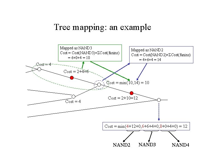
Tree mapping: an example Mapped as NAND 3 Cost = Cost(NAND 3)+ Cost(fanins) = 6+0+4 = 10 Cost = 4 Mapped as NAND 2 Cost = Cost(NAND 2)+ Cost(fanins) = 4+6+4 = 14 Cost = 2+4=6 Cost = min(10, 14) = 10 Cost = 4 Cost = 2+10=12 Cost = min(4+12+0, 6+6+4+0, 8+0+4+0) = 12 NAND 3 NAND 4

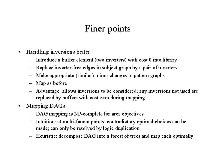
Finer points • Handling inversions better – – – Introduce a buffer element (two inverters) with cost 0 into library Replace inverter-free edges in subject graph by a pair of inverters Make appropriate (similar) minor changes to pattern graphs Map as before Advantage: allows inversions to be considered; any inversions not used are replaced by buffers with cost zero during mapping • Mapping DAGs – DAG mapping is NP-complete for area objectives – Intuition: at multi-fanout points, contradictory optimal choices can be made; can only be resolved by logic duplication – Heuristic: decompose DAG into a forest of trees and map each optimally

Circuit decomposition • Quality of mapping depends on decomposition of circuit – 2 NAND/NOT and AND/OR/NOT decompositions used most often – Number of such decompositions is huge! • Clever way of considering all decompositions proposed by Lehman, Watanabe, Grodstein and Harkness, IEEE Transactions on CAD 8/1997, pp. 813 -834

Other objective functions • Minimizing area considered – seen to be easy • Minimizing delay is more complex, since delay is fanoutdependent • Basic procedure for tree-mapping – Traverse graph as before – Store several best solutions at each node, parameterized by load capacitance values (i. e. , store best solution for several load caps) – This also allows mapper to use various power levels available for each cell in the library

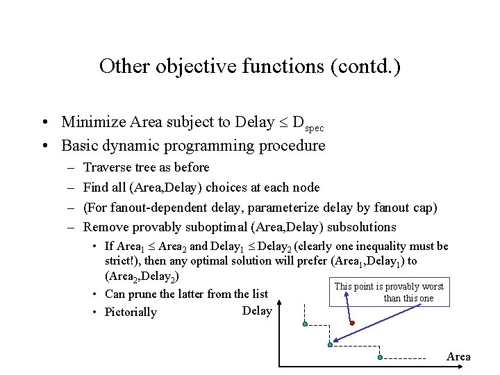
Other objective functions (contd. ) • Minimize Area subject to Delay Dspec • Basic dynamic programming procedure – – Traverse tree as before Find all (Area, Delay) choices at each node (For fanout-dependent delay, parameterize delay by fanout cap) Remove provably suboptimal (Area, Delay) subsolutions • If Area 1 Area 2 and Delay 1 Delay 2 (clearly one inequality must be strict!), then any optimal solution will prefer (Area 1, Delay 1) to (Area 2, Delay 2) This point is provably worst • Can prune the latter from the list than this one Delay • Pictorially Area

Final note on synthesis • Deep submicron technologies (< 0. 25 micron or so): – Wire capacitances are significant – Interconnect significantly affects circuit performance • Traditional wire-load models – Fanout load depends on # fanouts, calculated statistically – Invalid in deep submicron since fanout RC’s depend on locations and not just number of fanouts • Physical synthesis – Concurrently perform placement and synthesis – Common approach • Create “physical prototype” – coarse placement • Perform synthesis according to this placement; refine placement as you go along