Logic Gates and other Complex gates Switch logic

- Slides: 52

Logic Gates and other Complex gates, Switch logic, Alternate gate circuits Physical Design, Floor Planning, Placement – Routing, Power Delay Estimation, Clock and Power Routing

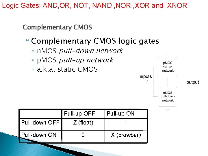
Logic Gates: AND, OR, NOT, NAND , NOR , XOR and XNOR Complementary CMOS logic gates ◦ n. MOS pull-down network ◦ p. MOS pull-up network ◦ a. k. a. static CMOS Pull-up OFF Pull-up ON Pull-down OFF Z (float) 1 Pull-down ON 0 X (crowbar)

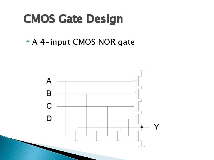
CMOS Gate Design A 4 -input CMOS NOR gate

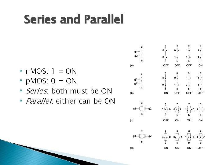
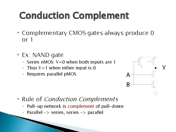
Series and Parallel n. MOS: 1 = ON p. MOS: 0 = ON Series: both must be ON Parallel: either can be ON

Conduction Complementary CMOS gates always produce 0 or 1 Ex: NAND gate ◦ Series n. MOS: Y=0 when both inputs are 1 ◦ Thus Y=1 when either input is 0 ◦ Requires parallel p. MOS Rule of Conduction Complements ◦ Pull-up network is complement of pull-down ◦ Parallel -> series, series -> parallel

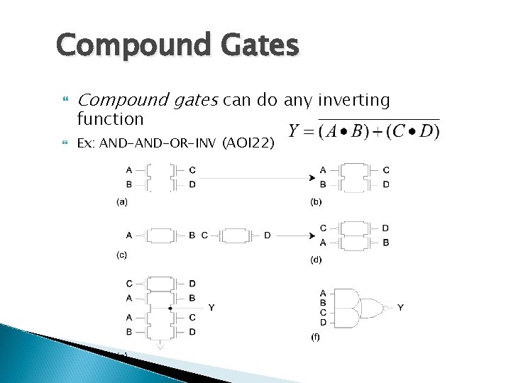
Compound Gates Compound gates can do any inverting Ex: AND-OR-INV (AOI 22) function

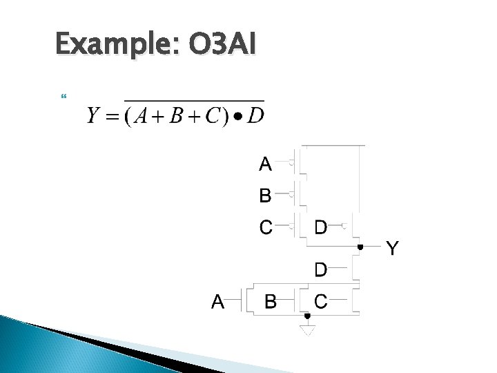
Example: O 3 AI

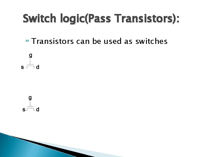
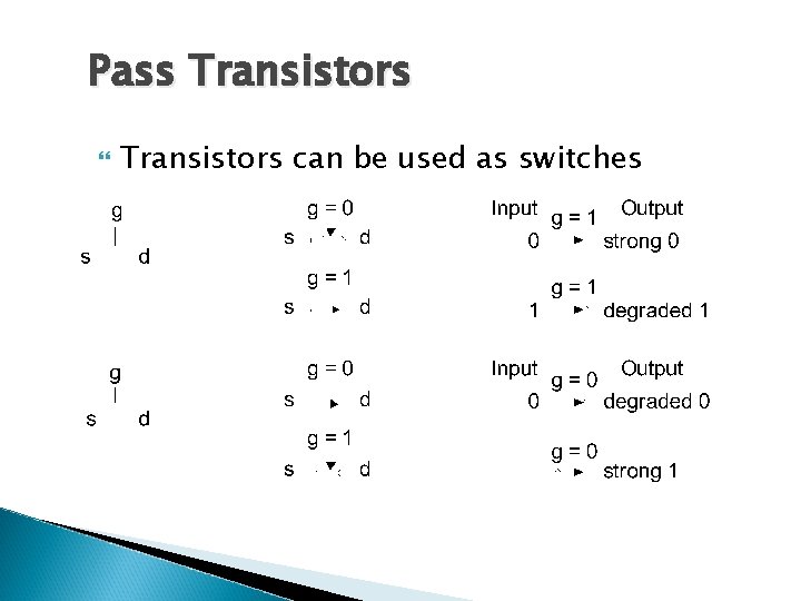
Switch logic(Pass Transistors): Transistors can be used as switches

Pass Transistors can be used as switches

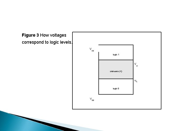
Figure 3 How voltages correspond to logic levels. VDD logic 1 VH unknown (X) VL logic 0 VSS

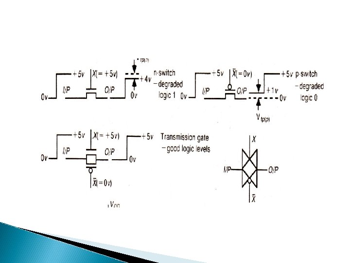
Signal Strength of signal ◦ How close it approximates ideal voltage source VDD and GND rails are strongest 1 and 0 n. MOS pass strong 0 ◦ But degraded or weak 1 p. MOS pass strong 1 ◦ But degraded or weak 0 Thus NMOS are best for pull-down network Thus PMOS are best for pull-up network


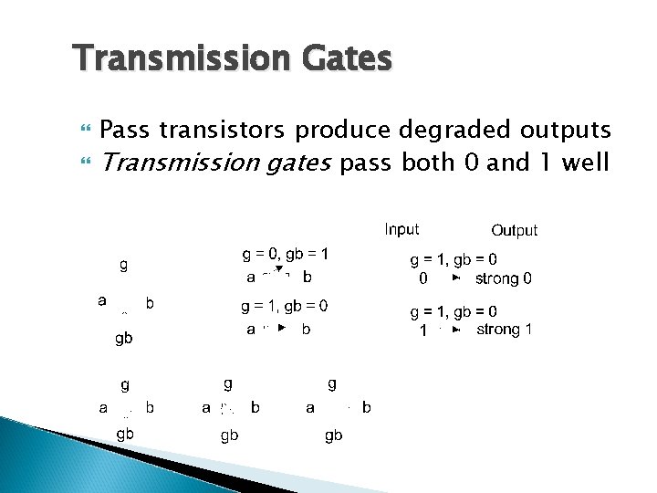
Transmission Gates Pass transistors produce degraded outputs Transmission gates pass both 0 and 1 well

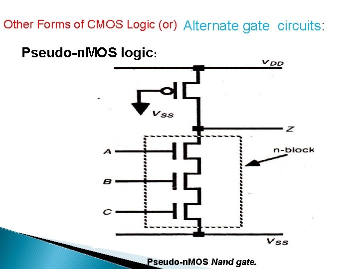
Other Forms of CMOS Logic (or) Alternate gate circuits: Pseudo-n. MOS logic: Pseudo-n. MOS Nand gate.

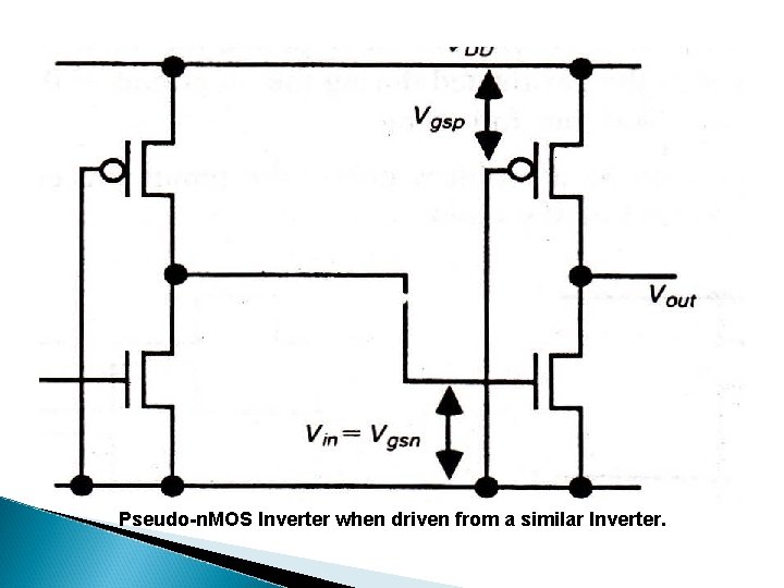
Pseudo-n. MOS Inverter when driven from a similar Inverter.

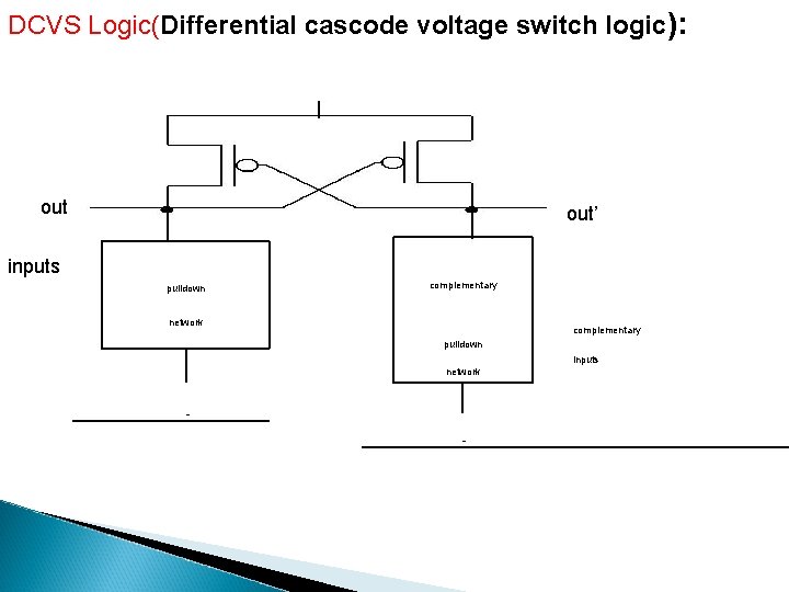
DCVS Logic(Differential cascode voltage switch logic): out’ inputs pulldown complementary network complementary pulldown inputs network -

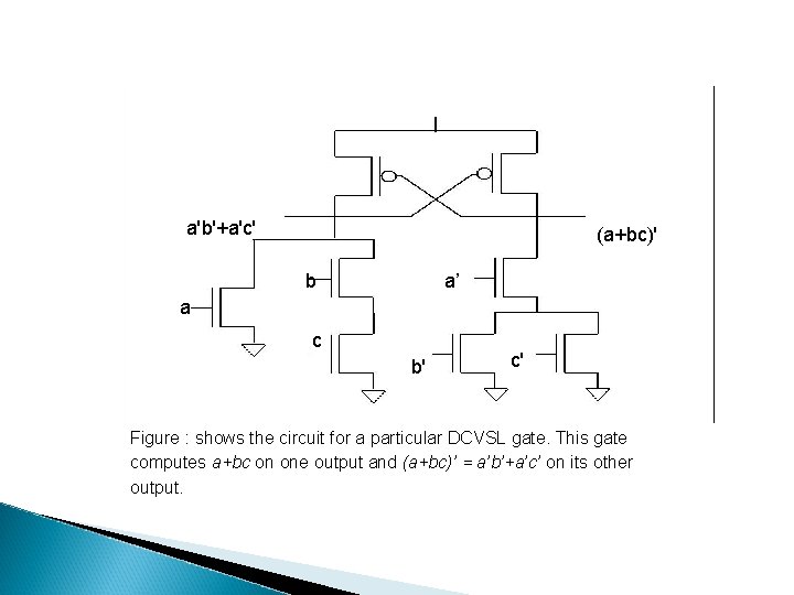
a'b'+a'c' (a+bc)' b a’ a c b' c' Figure : shows the circuit for a particular DCVSL gate. This gate computes a+bc on one output and (a+bc)’ = a’b’+a’c’ on its other output.

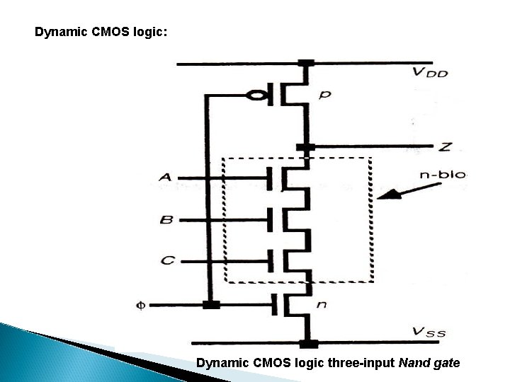
Dynamic CMOS logic: Dynamic CMOS logic three-input Nand gate

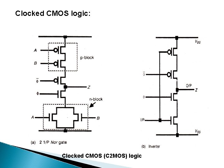
Clocked CMOS logic: Clocked CMOS (C 2 MOS) logic

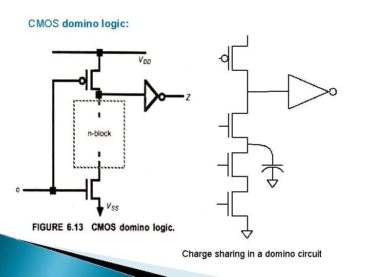
CMOS domino logic: Charge sharing in a domino circuit

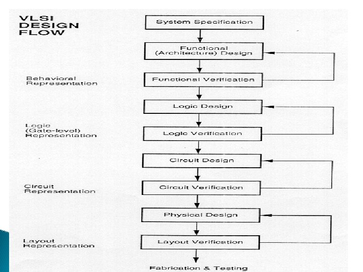
Physical Design 21

22

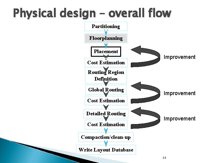
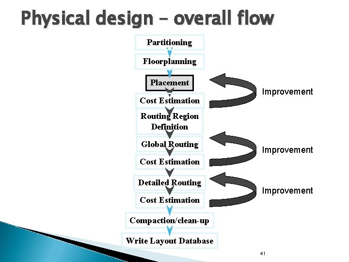
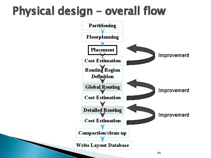
Physical design – overall flow Partitioning Floorplanning Placement Cost Estimation Improvement Routing Region Definition Global Routing Improvement Cost Estimation Detailed Routing Cost Estimation Improvement Compaction/clean-up Write Layout Database 23

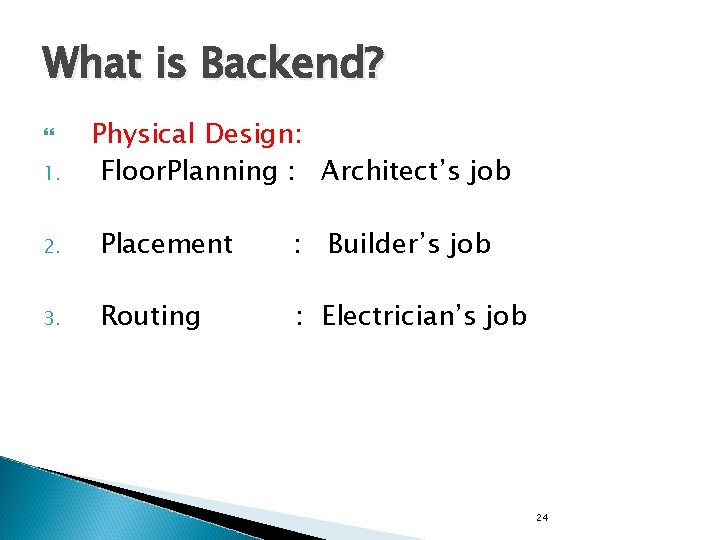
What is Backend? 1. Physical Design: Floor. Planning : Architect’s job 2. Placement : Builder’s job 3. Routing : Electrician’s job 24

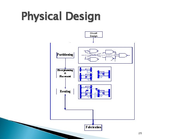
Physical Design Circuit Design Partitioning Floorplanning & Placement Routing Fabrication 25

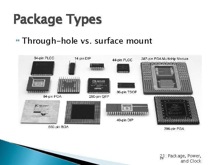
Package Types Through-hole vs. surface mount 21: Package, Power, and Clock 26

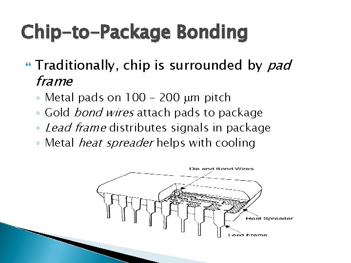
Chip-to-Package Bonding Traditionally, chip is surrounded by pad frame ◦ ◦ Metal pads on 100 – 200 mm pitch Gold bond wires attach pads to package Lead frame distributes signals in package Metal heat spreader helps with cooling

Partitioning: Decompose a large complex system into smaller subsystems Decompose hierarchically until each subsystem is of manageable size Design each subsystem separately to speed up the process Minimize connection between two subsystems to reduce interdependency 28

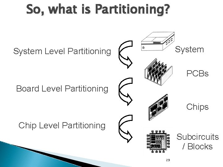
So, what is Partitioning? System Level Partitioning PCBs Board Level Partitioning Chips Chip Level Partitioning Subcircuits / Blocks 29

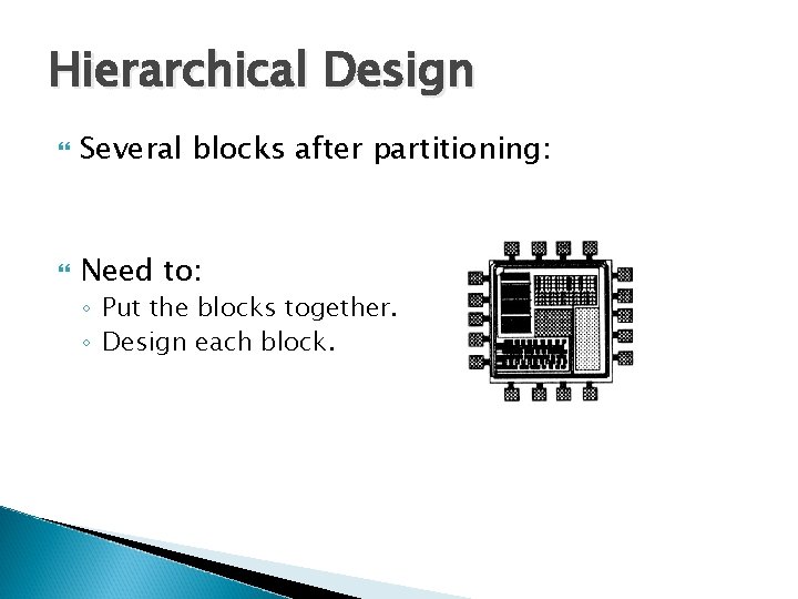
Hierarchical Design Several blocks after partitioning: Need to: ◦ Put the blocks together. ◦ Design each block.

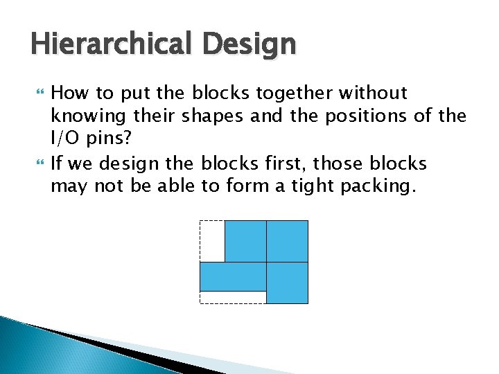
Hierarchical Design How to put the blocks together without knowing their shapes and the positions of the I/O pins? If we design the blocks first, those blocks may not be able to form a tight packing.

Partitioning methods Top-down partitioning ◦ ◦ ◦ Iterative improvement Spectral based Clustering methods Network flow based Analytical based Multi-level Bottom-up clustering ◦ Unit delay model ◦ General delay model ◦ Sequential circuits with retiming 32

Floorplanning: The floorplanning problem is to plan the positions and shapes of the modules at the beginning of the design cycle to optimize the circuit performance ◦ ◦ ◦ chip area total wirelength delay of critical path routability others, e. g. , noise, heat dissipation, etc.

Floorplanning v. s. Placement Both determines block positions to optimize the circuit performance. Floorplanning: ◦ Details like shapes of blocks, I/O pin positions, etc. are not yet fixed (blocks with flexible shape are called soft blocks). Placement: ◦ Details like module shapes and I/O pin positions are fixed (blocks with no flexibility in shape are called hard blocks).

Floorplanning: Output from partitioning used for floorplanning Inputs: ◦ Blocks with well-defined shapes and area ◦ Blocks with approximated area and no particular shape ◦ Netlist specifying block connections Outputs: ◦ Locations for all blocks 35

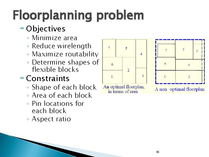
Floorplanning problem Objectives ◦ ◦ Minimize area Reduce wirelength Maximize routability Determine shapes of flexible blocks Constraints ◦ Shape of each block ◦ Area of each block ◦ Pin locations for each block ◦ Aspect ratio 36

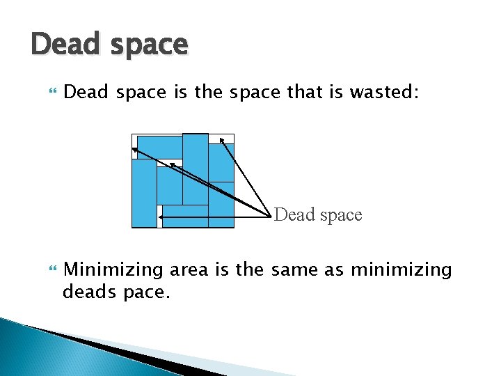
Dead space is the space that is wasted: Dead space Minimizing area is the same as minimizing deads pace.

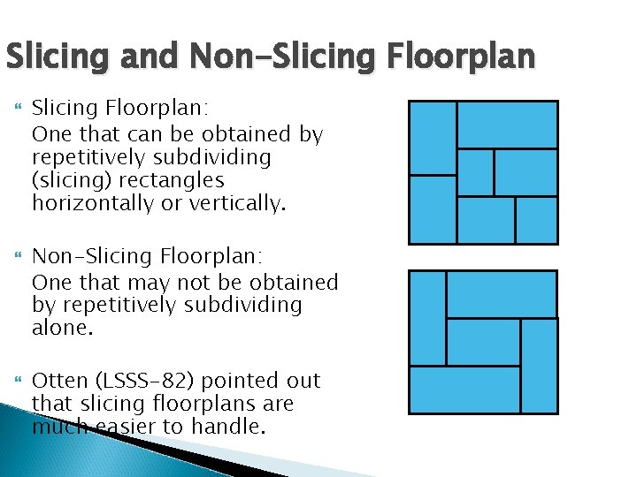
Slicing and Non-Slicing Floorplan Slicing Floorplan: One that can be obtained by repetitively subdividing (slicing) rectangles horizontally or vertically. Non-Slicing Floorplan: One that may not be obtained by repetitively subdividing alone. Otten (LSSS-82) pointed out that slicing floorplans are much easier to handle.

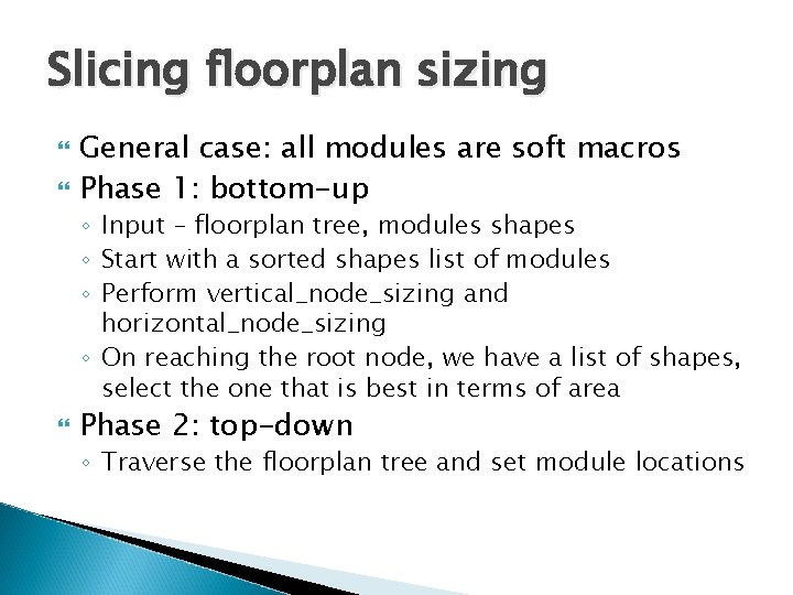
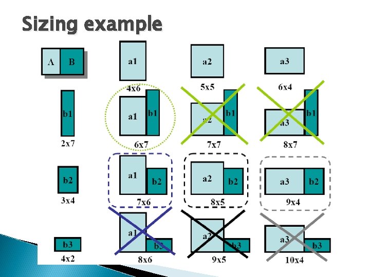
Slicing floorplan sizing General case: all modules are soft macros Phase 1: bottom-up ◦ Input – floorplan tree, modules shapes ◦ Start with a sorted shapes list of modules ◦ Perform vertical_node_sizing and horizontal_node_sizing ◦ On reaching the root node, we have a list of shapes, select the one that is best in terms of area Phase 2: top-down ◦ Traverse the floorplan tree and set module locations

Sizing example

Physical design – overall flow Partitioning Floorplanning Placement Cost Estimation Improvement Routing Region Definition Global Routing Improvement Cost Estimation Detailed Routing Cost Estimation Improvement Compaction/clean-up Write Layout Database 41

Placement The process of arranging circuit components on a layout surface Inputs : Set of fixed modules, netlist Output : Best position for each module based on various cost functions Cost functions include wirelength, wire routability, hotspots, performance, I/O pads

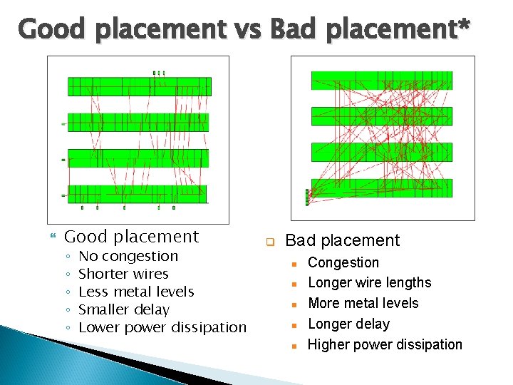
Good placement vs Bad placement* Good placement ◦ ◦ ◦ No congestion Shorter wires Less metal levels Smaller delay Lower power dissipation q Bad placement n n n Congestion Longer wire lengths More metal levels Longer delay Higher power dissipation

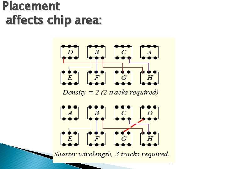
Placement affects chip area: 44

Physical design – overall flow Partitioning Floorplanning Placement Cost Estimation Improvement Routing Region Definition Global Routing Improvement Cost Estimation Detailed Routing Cost Estimation Improvement Compaction/clean-up Write Layout Database 45

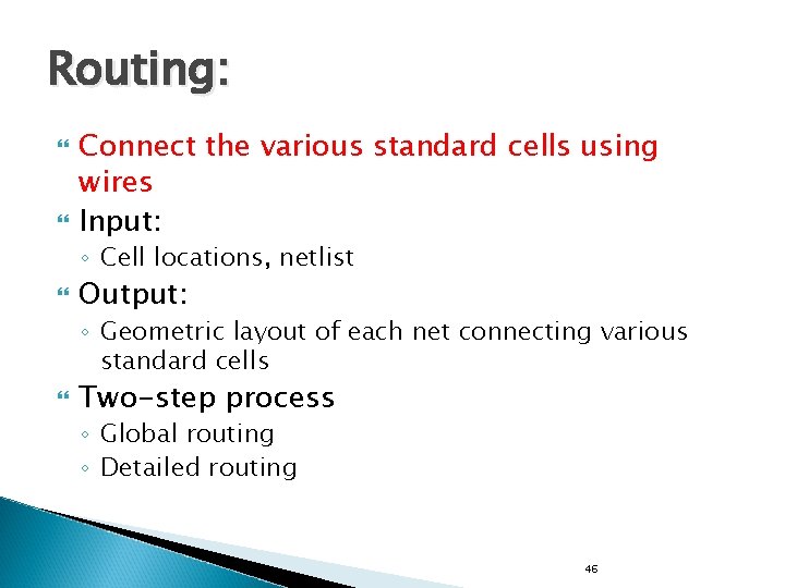
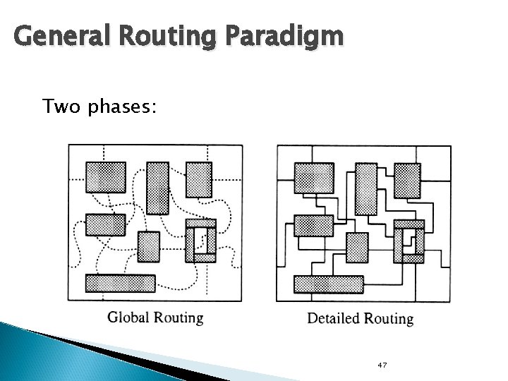
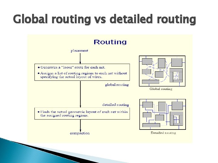
Routing: Connect the various standard cells using wires Input: ◦ Cell locations, netlist Output: ◦ Geometric layout of each net connecting various standard cells Two-step process ◦ Global routing ◦ Detailed routing 46

General Routing Paradigm Two phases: 47

Global routing vs detailed routing

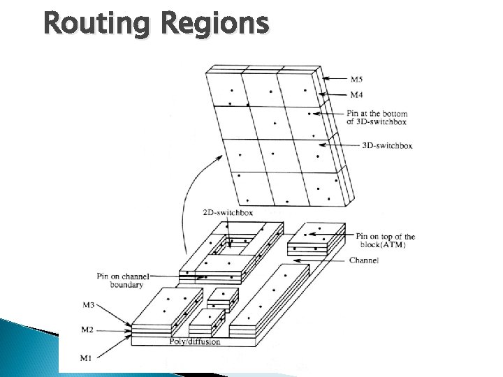
Routing Regions 49

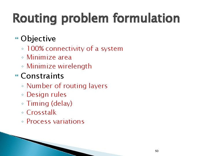
Routing problem formulation Objective ◦ 100% connectivity of a system ◦ Minimize area ◦ Minimize wirelength Constraints ◦ ◦ ◦ Number of routing layers Design rules Timing (delay) Crosstalk Process variations 50

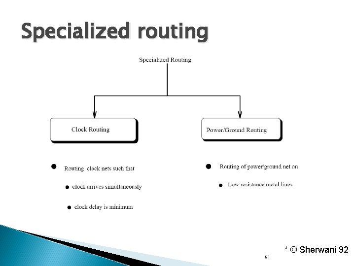
Specialized routing 51 * © Sherwani 92

Summary Looked at the physical design flow Involved several steps ◦ ◦ Partitioning Floorplanning Placement Routing Each step can be formulated as an optimization problem Need to go through 2 or more iterations in each step to generate an optimized solution 52