Logic Gates 1 Timing Issues 2 Specifying Logic
- Slides: 23

Logic Gates 1. Timing Issues 2. Specifying Logic Functions 3. Logic Design + =? Handouts: Lecture Slides 1

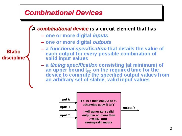
Combinational Devices Static discipline A combinational device is a circuit element that has – one or more digital inputs – one or more digital outputs – a functional specification that details the value of each output for every possible combination of valid input values – a timing specification consisting (at minimum) of an upper bound t. PD on the required time for the device to compute the specified output values from an arbitrary set of stable, valid input values input A input B input C If C is 1 then copy A to Y, otherwise copy B to Y output Y I will generate a valid output in no more than 2 weeks after seeing valid inputs 2

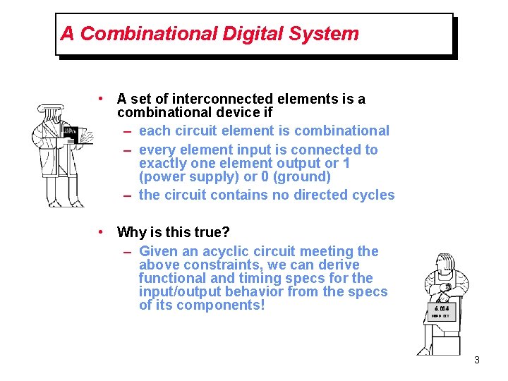
A Combinational Digital System • A set of interconnected elements is a combinational device if – each circuit element is combinational – every element input is connected to exactly one element output or 1 (power supply) or 0 (ground) – the circuit contains no directed cycles • Why is this true? – Given an acyclic circuit meeting the above constraints, we can derive functional and timing specs for the input/output behavior from the specs of its components! 3

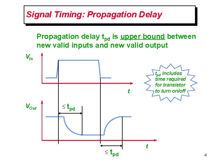
Signal Timing: Propagation Delay Propagation delay tpd is upper bound between new valid inputs and new valid output VIn tpd includes time required for transistor to turn on/off t VOut tpd t 4

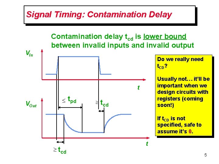
Signal Timing: Contamination Delay Contamination delay tcd is lower bound between invalid inputs and invalid output VIn Do we really need t. CD? Usually not… it’ll be important when we design circuits with registers (coming soon!) t tpd VOut tcd If t. CD is not specified, safe to assume it’s 0. tcd t 5

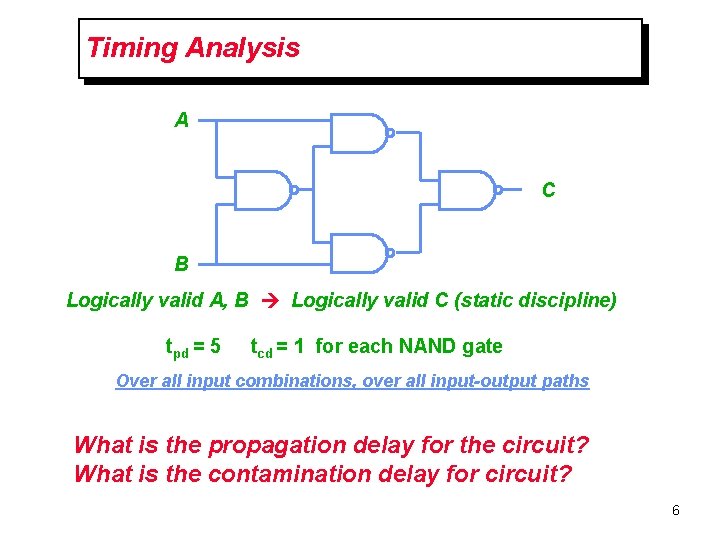
Timing Analysis A C B Logically valid A, B Logically valid C (static discipline) tpd = 5 tcd = 1 for each NAND gate Over all input combinations, over all input-output paths What is the propagation delay for the circuit? What is the contamination delay for circuit? 6

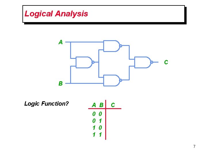
Logical Analysis A C B Logic Function? A B 0 0 1 1 C 0 1 7

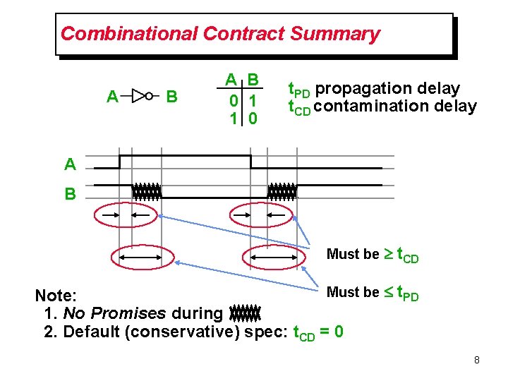
Combinational Contract Summary A B 0 1 1 0 t. PD propagation delay t. CD contamination delay A B Must be ³ t. CD Must be £ t. PD Note: 1. No Promises during 2. Default (conservative) spec: t. CD = 0 8

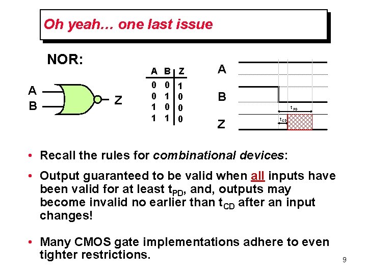
Oh yeah… one last issue NOR: A B Z Z 0 0 1 1 0 0 0 A B t. PD Z t. CD • Recall the rules for combinational devices: • Output guaranteed to be valid when all inputs have been valid for at least t. PD, and, outputs may become invalid no earlier than t. CD after an input changes! • Many CMOS gate implementations adhere to even tighter restrictions. 9

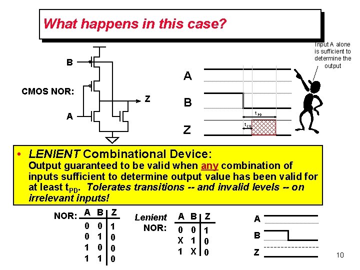
What happens in this case? Input A alone is sufficient to determine the output B A CMOS NOR: Z B t. PD A Z t. CD • LENIENT Combinational Device: Output guaranteed to be valid when any combination of inputs sufficient to determine output value has been valid for at least t. PD. Tolerates transitions -- and invalid levels -- on irrelevant inputs! NOR: A 0 0 1 1 B Z 0 1 1 0 0 0 Lenient NOR: A B Z 0 0 1 X 1 0 1 X 0 A B Z 10

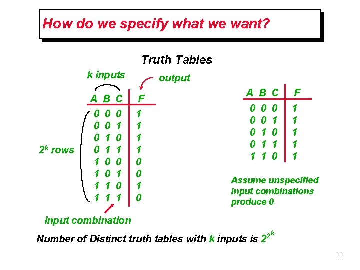
How do we specify what we want? Truth Tables k inputs A B C 2 k rows 0 0 1 1 0 1 0 1 output F 1 1 0 0 1 0 A B C 0 0 1 1 1 0 1 0 F 1 1 1 Assume unspecified input combinations produce 0 input combination Number of Distinct truth tables with k inputs is 2 2 k 11

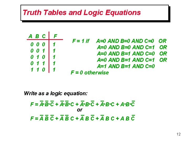
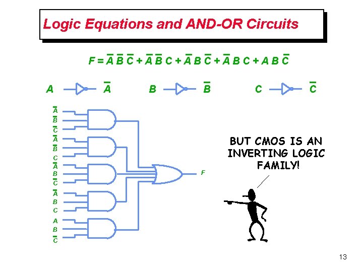
Truth Tables and Logic Equations A B C 0 0 1 1 1 0 1 0 F 1 1 1 F = 1 if A=0 AND B=0 AND C=0 AND B=0 AND C=1 A=0 AND B=1 AND C=0 AND B=1 AND C=1 AND B=1 AND C=0 F = 0 otherwise OR OR Write as a logic equation: F=ABC+ABC+ABC or F=ABC+ABC+ABC 12

Logic Equations and AND-OR Circuits F=ABC+ABC+ABC A A B B C C A B F BUT CMOS IS AN INVERTING LOGIC FAMILY! C A B C 13

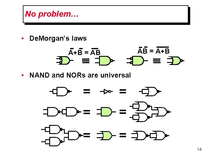
No problem… • De. Morgan’s laws AB = A+B = AB • NAND and NORs are universal = = = 14

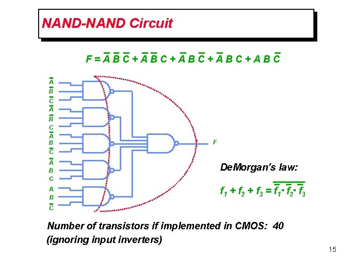
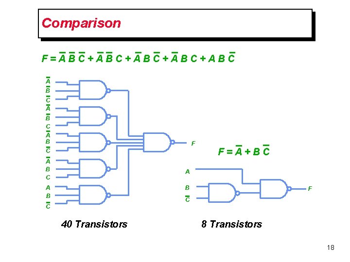
NAND-NAND Circuit F=ABC+ABC+ABC A B F C A B C De. Morgan’s law: A B f 1 + f 2 + f 3 = f 1 f 2 f 3 C Number of transistors if implemented in CMOS: 40 (ignoring input inverters) 15

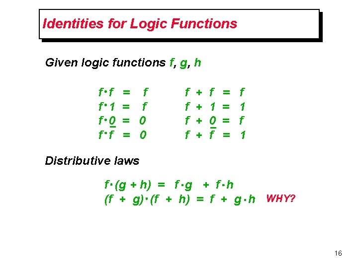
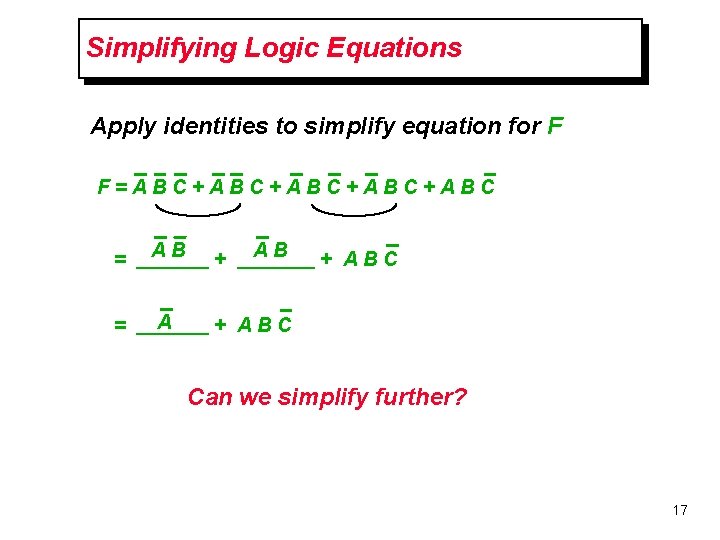
Identities for Logic Functions Given logic functions f, g, h f f f 1 0 f = f = 0 f f + + f 1 0 f = = f 1 Distributive laws f (g + h) = f g + f h (f + g) (f + h) = f + g h WHY? 16

Simplifying Logic Equations Apply identities to simplify equation for F F=ABC+ABC+ABC = AB = A + ABC Can we simplify further? 17

Comparison F=ABC+ABC+ABC A B F C A B C F=A+BC A A B B F C C 40 Transistors 8 Transistors 18

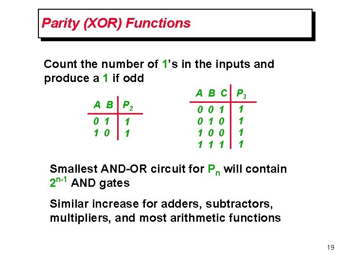
Parity (XOR) Functions Count the number of 1’s in the inputs and produce a 1 if odd A B P 2 0 1 1 A B C P 3 0 0 1 1 0 0 1 1 1 Smallest AND-OR circuit for Pn will contain 2 n-1 AND gates Similar increase for adders, subtractors, multipliers, and most arithmetic functions 19

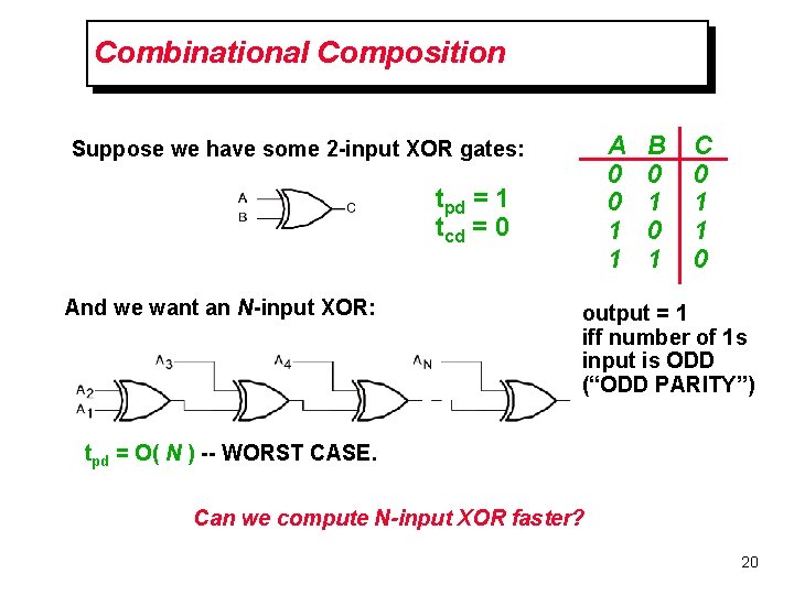
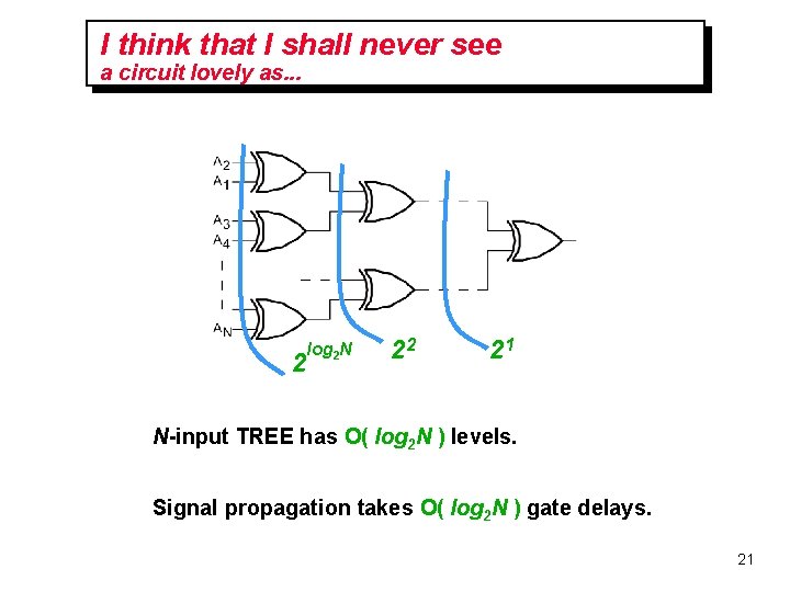
Combinational Composition A 0 0 1 1 Suppose we have some 2 -input XOR gates: tpd = 1 tcd = 0 And we want an N-input XOR: B 0 1 C 0 1 1 0 output = 1 iff number of 1 s input is ODD (“ODD PARITY”) tpd = O( N ) -- WORST CASE. Can we compute N-input XOR faster? 20

I think that I shall never see a circuit lovely as. . . 2 log 2 N 22 21 N-input TREE has O( log 2 N ) levels. Signal propagation takes O( log 2 N ) gate delays. 21

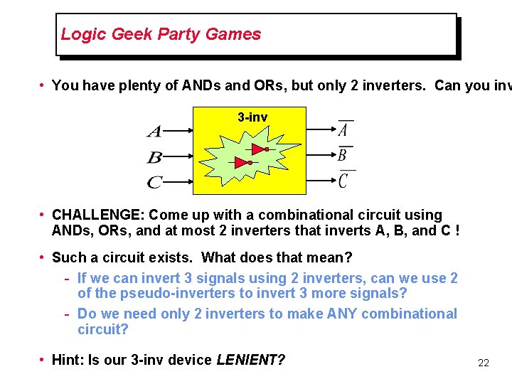
Logic Geek Party Games • You have plenty of ANDs and ORs, but only 2 inverters. Can you inv 3 -inv • CHALLENGE: Come up with a combinational circuit using ANDs, ORs, and at most 2 inverters that inverts A, B, and C ! • Such a circuit exists. What does that mean? - If we can invert 3 signals using 2 inverters, can we use 2 of the pseudo-inverters to invert 3 more signals? - Do we need only 2 inverters to make ANY combinational circuit? • Hint: Is our 3 -inv device LENIENT? 22

Next Time: Logic Synthesis Dilbert : S. Adams 23