Logic Design of Asynchronous Circuits Jordi Cortadella Univ


- Slides: 47

Logic Design of Asynchronous Circuits Jordi Cortadella Univ. Politècnica de Catalunya, Barcelona, Spain Jim Garside Manchester University, UK University of Newcastle upon Tyne, UK Alex Yakovlev 1

Outline • I: Basic concepts on asynchronous circuit design • II: Logic synthesis from concurrent specifications • III: Advanced topics on synthesis • IV: Design practice ASPDAC / VLSI 2002 - Tutorial on Logic Design of Asynchronous Circuits 2

Logic Design of Asynchronous Circuits Part I: Basic concepts on asynchronous circuit design 3

Outline • • • What is an asynchronous circuit ? Asynchronous communication Async Design Styles (Micropipelines, …) Asynchronous logic building blocks Control specification and implementation Delay models and classes of async circuits • Why asynchronous circuits ? ASPDAC / VLSI 2002 - Tutorial on Logic Design of Asynchronous Circuits 4

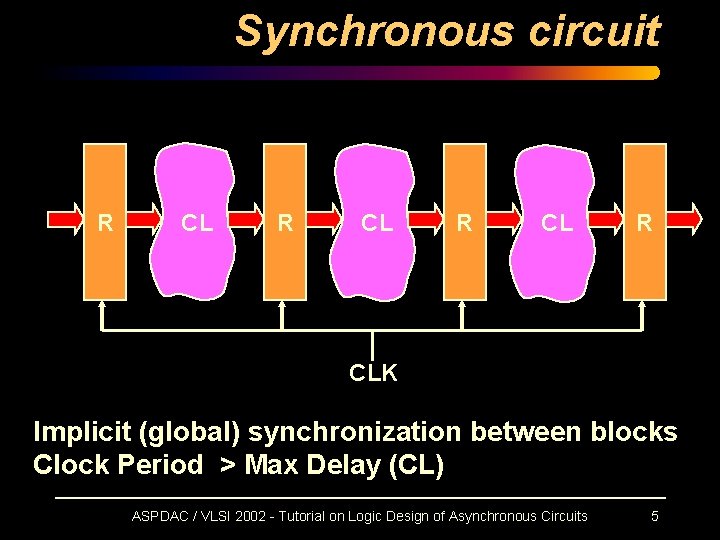
Synchronous circuit R CLK Implicit (global) synchronization between blocks Clock Period > Max Delay (CL) ASPDAC / VLSI 2002 - Tutorial on Logic Design of Asynchronous Circuits 5

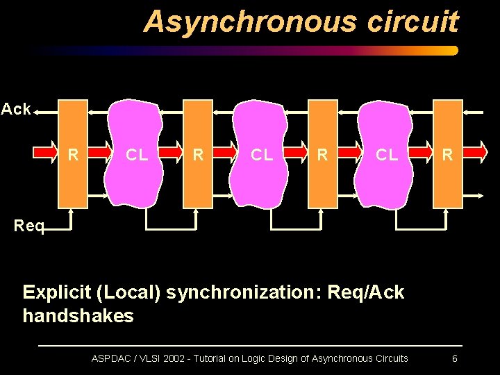
Asynchronous circuit Ack R CL R Req Explicit (Local) synchronization: Req/Ack handshakes ASPDAC / VLSI 2002 - Tutorial on Logic Design of Asynchronous Circuits 6

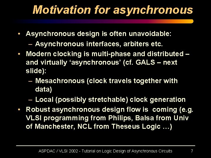
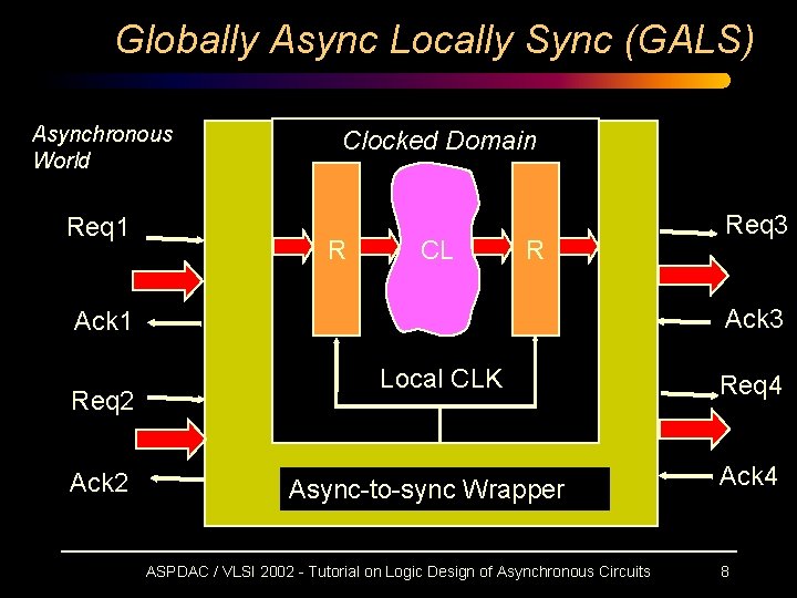
Motivation for asynchronous • Asynchronous design is often unavoidable: – Asynchronous interfaces, arbiters etc. • Modern clocking is multi-phase and distributed – and virtually ‘asynchronous’ (cf. GALS – next slide): – Mesachronous (clock travels together with data) – Local (possibly stretchable) clock generation • Robust asynchronous design flow is coming (e. g. VLSI programming from Philips, Balsa from Univ of Manchester, NCL from Theseus Logic …) ASPDAC / VLSI 2002 - Tutorial on Logic Design of Asynchronous Circuits 7

Globally Async Locally Sync (GALS) Asynchronous World Req 1 Clocked Domain R CL R Ack 3 Ack 1 Req 2 Ack 2 Req 3 Local CLK Async-to-sync Wrapper ASPDAC / VLSI 2002 - Tutorial on Logic Design of Asynchronous Circuits Req 4 Ack 4 8

Key Design Differences • Synchronous logic design: – proceeds without taking timing correctness (hazards, signal ack-ing etc. ) into account – Combinational logic and memory latches (registers) are built separately – Static timing analysis of CL is sufficient to determine the Max Delay (clock period) – Fixed set-up and hold conditions for latches ASPDAC / VLSI 2002 - Tutorial on Logic Design of Asynchronous Circuits 9

Key Design Differences • Asynchronous logic design: – Must ensure hazard-freedom, signal ack-ing, local timing constraints – Combinational logic and memory latches (registers) are often mixed in “complex gates” – Dynamic timing analysis of logic is needed to determine relative delays between paths • To avoid complex issues, circuits may be built as Delay-insensitive and/or Speedindependent (as discussed later) ASPDAC / VLSI 2002 - Tutorial on Logic Design of Asynchronous Circuits 10

Verification and Testing Differences • Synchronous logic verification and testing: – Only functional correctness aspect is verified and tested – Testing can be done with standard ATE and at low speed • Asynchronous logic verification and testing: – In addition to functional correctness, temporal aspect is crucial: e. g. causality and order, deadlock-freedom – Testing must cover faults in complex gates (logic+memory) and must proceed at normal operation rate – Delay fault testing may be needed ASPDAC / VLSI 2002 - Tutorial on Logic Design of Asynchronous Circuits 11

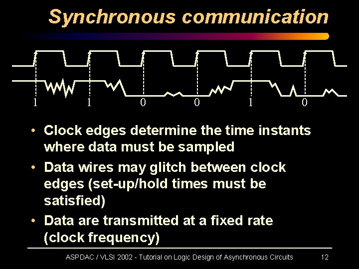
Synchronous communication 1 1 0 0 1 0 • Clock edges determine the time instants where data must be sampled • Data wires may glitch between clock edges (set-up/hold times must be satisfied) • Data are transmitted at a fixed rate (clock frequency) ASPDAC / VLSI 2002 - Tutorial on Logic Design of Asynchronous Circuits 12

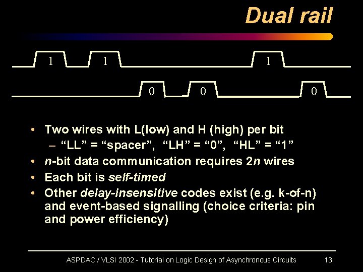
Dual rail 1 1 1 0 0 0 • Two wires with L(low) and H (high) per bit – “LL” = “spacer”, “LH” = “ 0”, “HL” = “ 1” • n-bit data communication requires 2 n wires • Each bit is self-timed • Other delay-insensitive codes exist (e. g. k-of-n) and event-based signalling (choice criteria: pin and power efficiency) ASPDAC / VLSI 2002 - Tutorial on Logic Design of Asynchronous Circuits 13

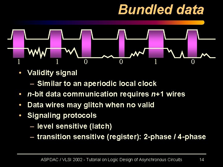
Bundled data 1 1 0 0 1 0 • Validity signal – Similar to an aperiodic local clock • n-bit data communication requires n+1 wires • Data wires may glitch when no valid • Signaling protocols – level sensitive (latch) – transition sensitive (register): 2 -phase / 4 -phase ASPDAC / VLSI 2002 - Tutorial on Logic Design of Asynchronous Circuits 14

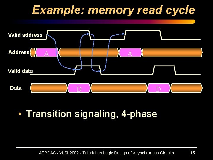
Example: memory read cycle Valid address A A Valid data D D • Transition signaling, 4 -phase ASPDAC / VLSI 2002 - Tutorial on Logic Design of Asynchronous Circuits 15

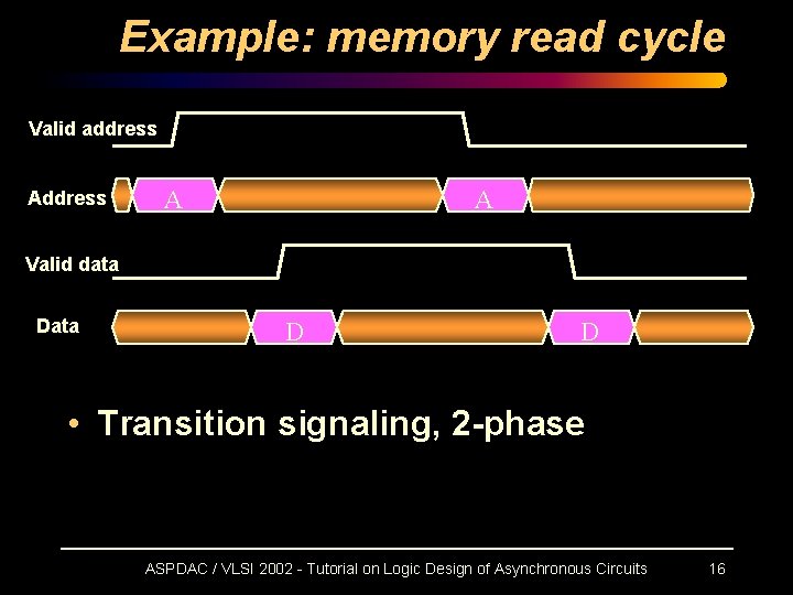
Example: memory read cycle Valid address A A Valid data D D • Transition signaling, 2 -phase ASPDAC / VLSI 2002 - Tutorial on Logic Design of Asynchronous Circuits 16

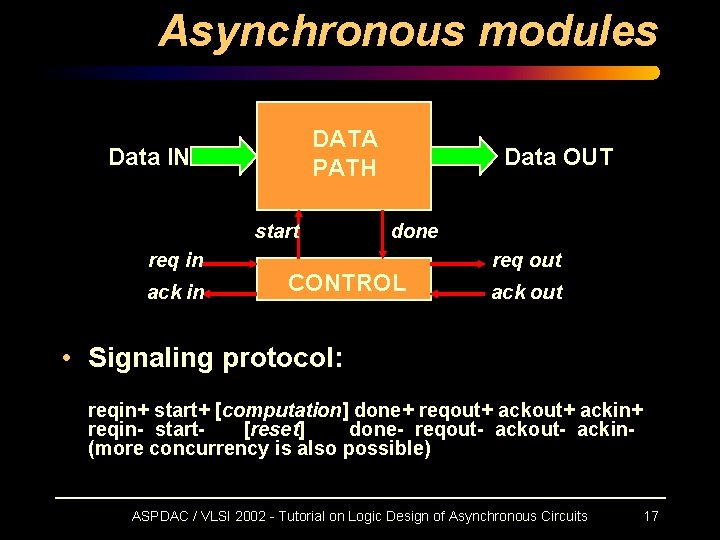
Asynchronous modules DATA PATH Data IN start req in ack in Data OUT done CONTROL req out ack out • Signaling protocol: reqin+ start+ [computation] done+ reqout+ ackin+ reqin- start[reset] done- reqout- ackin(more concurrency is also possible) ASPDAC / VLSI 2002 - Tutorial on Logic Design of Asynchronous Circuits 17

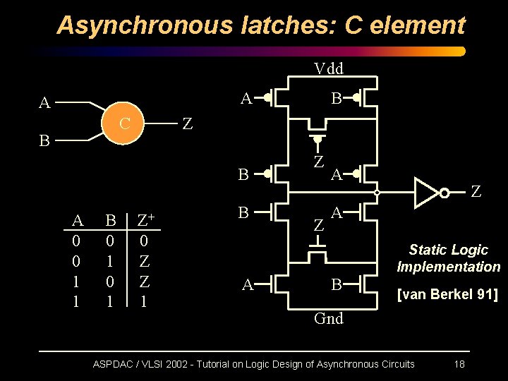
Asynchronous latches: C element Vdd A A C B Z B A 0 0 1 1 B 0 1 B Z+ 0 Z Z 1 B Z Z A Static Logic Implementation A B [van Berkel 91] Gnd ASPDAC / VLSI 2002 - Tutorial on Logic Design of Asynchronous Circuits 18

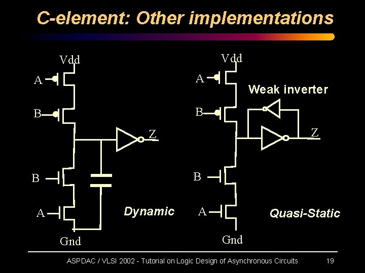
C-element: Other implementations Vdd A A B B Weak inverter Z Z B B Dynamic A Gnd A Quasi-Static Gnd ASPDAC / VLSI 2002 - Tutorial on Logic Design of Asynchronous Circuits 19

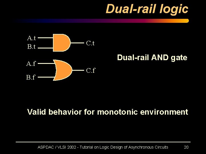
Dual-rail logic A. t B. t A. f B. f C. t Dual-rail AND gate C. f Valid behavior for monotonic environment ASPDAC / VLSI 2002 - Tutorial on Logic Design of Asynchronous Circuits 20

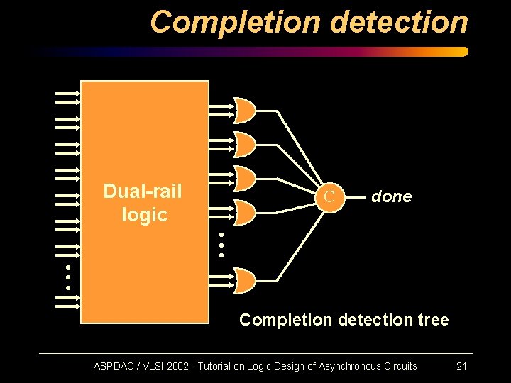
Completion detection Dual-rail logic • • • C done • • • Completion detection tree ASPDAC / VLSI 2002 - Tutorial on Logic Design of Asynchronous Circuits 21

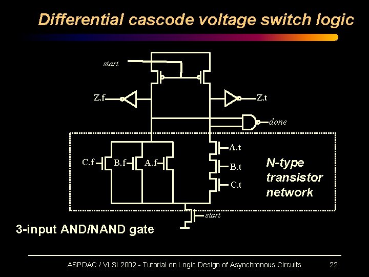
Differential cascode voltage switch logic start Z. f Z. t done A. t C. f B. f A. f B. t C. t N-type transistor network start 3 -input AND/NAND gate ASPDAC / VLSI 2002 - Tutorial on Logic Design of Asynchronous Circuits 22

Examples of dual-rail design • Asynchronous dual-rail ripple-carry adder (A. Martin, 1991) – Critical delay is proportional to log. N (N=number of bits) – 32 -bit adder delay (1. 6 m MOSIS CMOS): 11 ns versus 40 ns for synchronous – Async cell transistor count = 34 versus synchronous = 28 • More recent success stories (modularity and automatic synthesis) of dual-rail logic from Null-Convension Logic from Theseus Logic ASPDAC / VLSI 2002 - Tutorial on Logic Design of Asynchronous Circuits 23

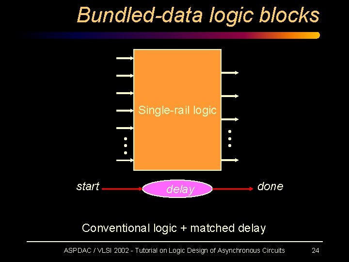
Bundled-data logic blocks Single-rail logic • • • start delay done Conventional logic + matched delay ASPDAC / VLSI 2002 - Tutorial on Logic Design of Asynchronous Circuits 24

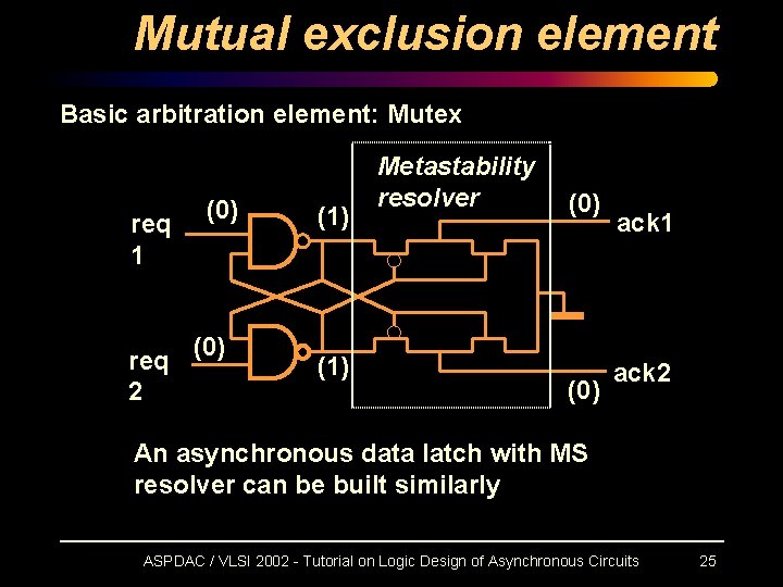
Mutual exclusion element Basic arbitration element: Mutex req 1 req 2 (0) (1) Metastability resolver (0) ack 1 ack 2 An asynchronous data latch with MS resolver can be built similarly ASPDAC / VLSI 2002 - Tutorial on Logic Design of Asynchronous Circuits 25

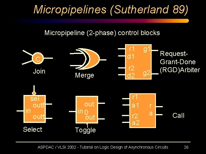
Micropipelines (Sutherland 89) Micropipeline (2 -phase) control blocks r 1 d 1 C Join sel outf in outt Select Merge out in 0 out 1 Toggle r 2 d 2 r 1 a 1 r 2 a 2 g 1 g 2 Request. Grant-Done (RGD)Arbiter r a ASPDAC / VLSI 2002 - Tutorial on Logic Design of Asynchronous Circuits Call 26

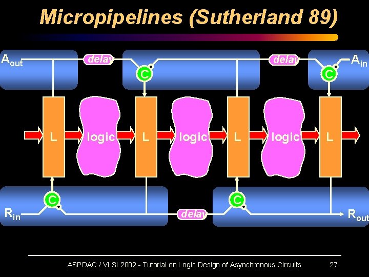
Micropipelines (Sutherland 89) Aout delay C L Rin delay logic L C logic C L logic Ain L C Rout delay ASPDAC / VLSI 2002 - Tutorial on Logic Design of Asynchronous Circuits 27

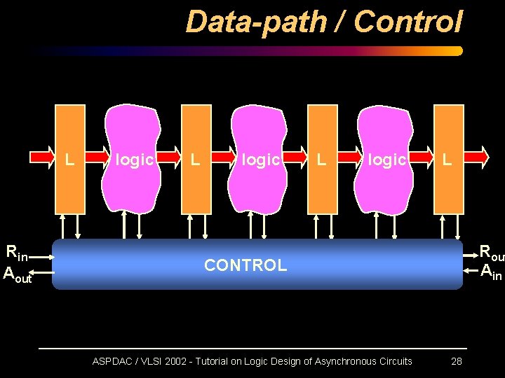
Data-path / Control L Rin Aout logic L Rout Ain CONTROL ASPDAC / VLSI 2002 - Tutorial on Logic Design of Asynchronous Circuits 28

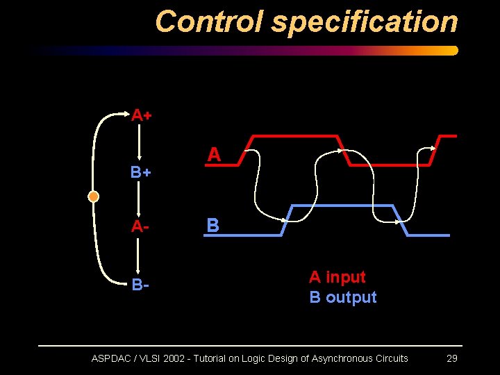
Control specification A+ B+ AB- A B A input B output ASPDAC / VLSI 2002 - Tutorial on Logic Design of Asynchronous Circuits 29

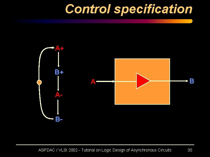
Control specification A+ B+ A B AB- ASPDAC / VLSI 2002 - Tutorial on Logic Design of Asynchronous Circuits 30

Control specification A+ BA B AB+ ASPDAC / VLSI 2002 - Tutorial on Logic Design of Asynchronous Circuits 31

Control specification A+ B+ A C+ C A- B- C B C- ASPDAC / VLSI 2002 - Tutorial on Logic Design of Asynchronous Circuits 32

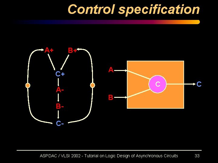
Control specification A+ B+ C+ A- A C C B BC- ASPDAC / VLSI 2002 - Tutorial on Logic Design of Asynchronous Circuits 33

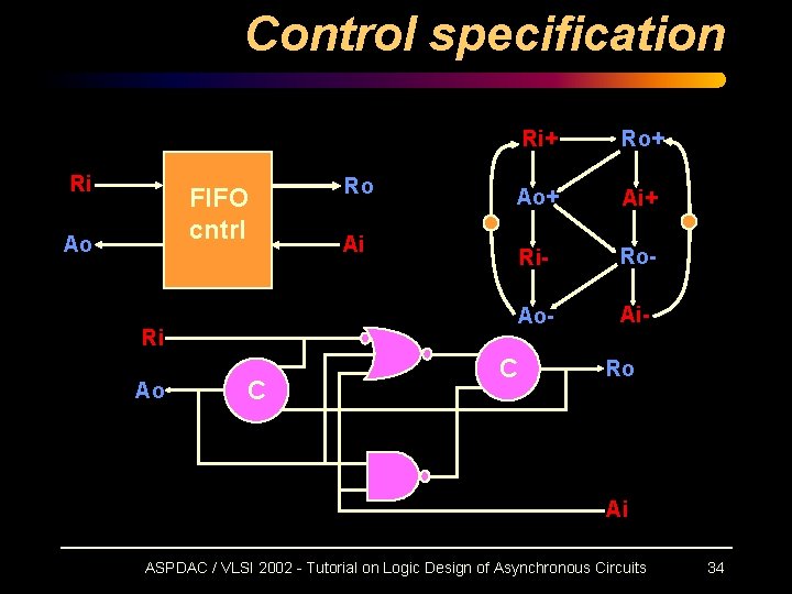
Control specification Ri FIFO cntrl Ao Ri Ao C Ro Ri+ Ro+ Ai+ Ri- Ro- Ai- Ai C Ro Ai ASPDAC / VLSI 2002 - Tutorial on Logic Design of Asynchronous Circuits 34

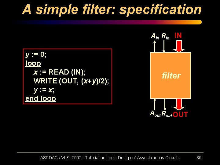
A simple filter: specification Ain Rin y : = 0; loop x : = READ (IN); WRITE (OUT, (x+y)/2); y : = x; end loop IN filter Aout Rout OUT ASPDAC / VLSI 2002 - Tutorial on Logic Design of Asynchronous Circuits 35

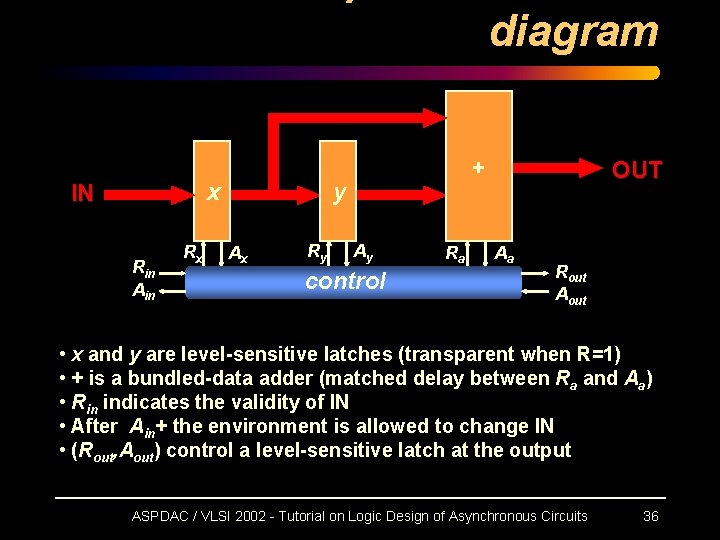
diagram x IN Rin Ain Rx + y Ax Ry Ay control Ra OUT Aa Rout Aout • x and y are level-sensitive latches (transparent when R=1) • + is a bundled-data adder (matched delay between Ra and Aa) • Rin indicates the validity of IN • After Ain+ the environment is allowed to change IN • (Rout, Aout) control a level-sensitive latch at the output ASPDAC / VLSI 2002 - Tutorial on Logic Design of Asynchronous Circuits 36

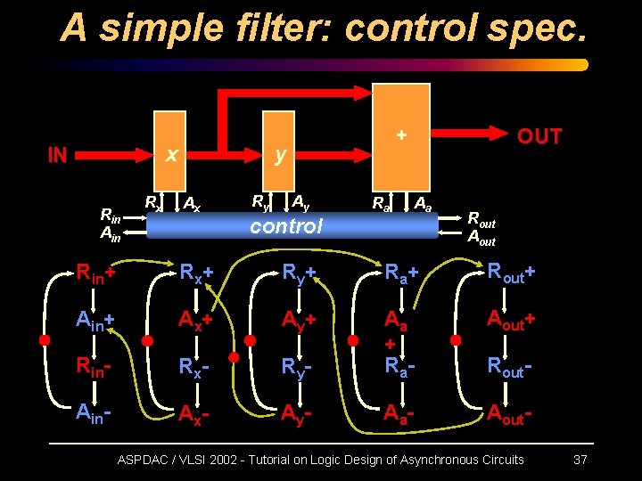
A simple filter: control spec. x IN Rin Ain Rx + y Ax Ry Ay control Ra OUT Aa Rout Aout Rin+ R x+ R y+ R a+ Rout+ Ain+ A x+ A y+ Aout+ Rin- R x- R y- Aa + R a- Rout- Ain- A x- A y- A a- Aout- ASPDAC / VLSI 2002 - Tutorial on Logic Design of Asynchronous Circuits 37

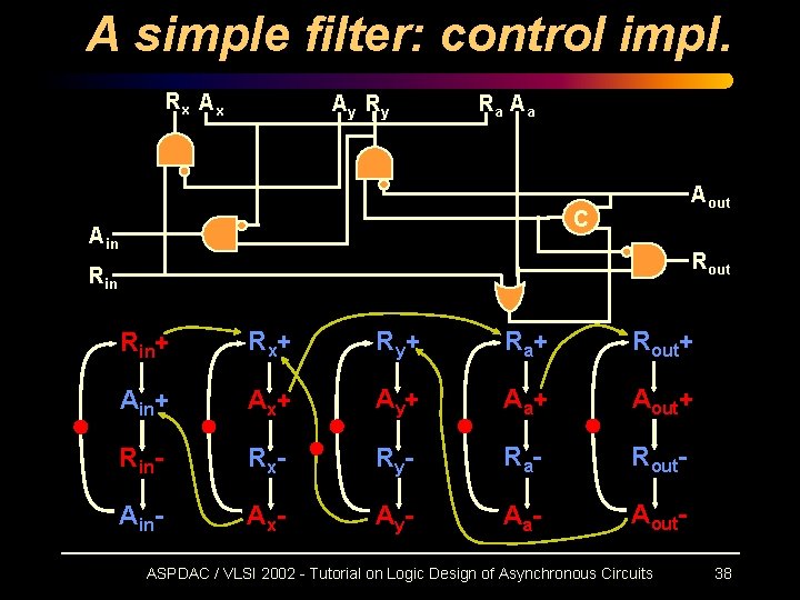
A simple filter: control impl. Rx Ax Ay Ry Ra Aa Aout C Ain Rout Rin+ R x+ R y+ R a+ Rout+ Ain+ A x+ A y+ A a+ Aout+ Rin- R x- R y- R a- Rout- Ain- A x- A y- A a- Aout- ASPDAC / VLSI 2002 - Tutorial on Logic Design of Asynchronous Circuits 38

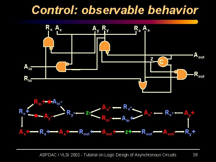
Control: observable behavior Rx Ax Ra Aa Ay Ry z Ain Aout C Rout Rin+ Rx + Ain- Ay Ra + Ry Aa + z. Rout+ Aa - Rin- Ain+ Aout+ z+ Ax - Rx - Ay + Rout- Aout- Ry + ASPDAC / VLSI 2002 - Tutorial on Logic Design of Asynchronous Circuits 39

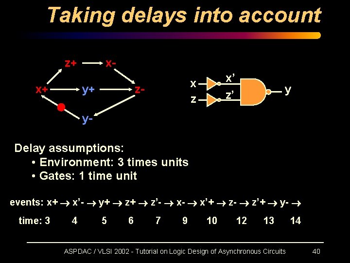
Taking delays into account z+ x+ xy+ x’ z’ x z z- y y. Delay assumptions: • Environment: 3 times units • Gates: 1 time unit events: x+ x’- y+ z’- x’+ z- z’+ y- time: 3 4 5 6 7 9 10 12 13 ASPDAC / VLSI 2002 - Tutorial on Logic Design of Asynchronous Circuits 14 40

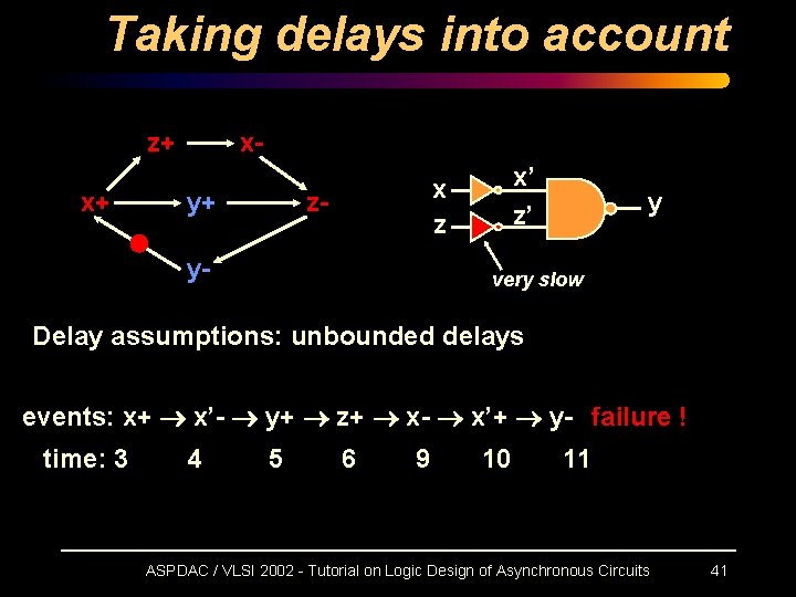
Taking delays into account z+ x+ xy+ x’ z’ x z z- y- y very slow Delay assumptions: unbounded delays events: x+ x’- y+ z+ x- x’+ y- failure ! time: 3 4 5 6 9 10 11 ASPDAC / VLSI 2002 - Tutorial on Logic Design of Asynchronous Circuits 41

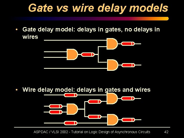
Gate vs wire delay models • Gate delay model: delays in gates, no delays in wires • Wire delay model: delays in gates and wires ASPDAC / VLSI 2002 - Tutorial on Logic Design of Asynchronous Circuits 42

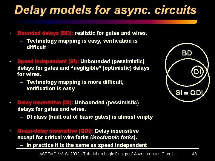
Delay models for async. circuits • • Bounded delays (BD): realistic for gates and wires. – Technology mapping is easy, verification is difficult Speed independent (SI): Unbounded (pessimistic) delays for gates and “negligible” (optimistic) delays for wires. – Technology mapping is more difficult, verification is easy • Delay insensitive (DI): Unbounded (pessimistic) delays for gates and wires. – DI class (built out of basic gates) is almost empty • Quasi-delay insensitive (QDI): Delay insensitive except for critical wire forks (isochronic forks). – In practice it is the same as speed independent BD DI SI QDI ASPDAC / VLSI 2002 - Tutorial on Logic Design of Asynchronous Circuits 43

Motivation (designer’s view) • Modularity for system-on-chip design – Plug-and-play interconnectivity • Average-case peformance – No worst-case delay synchronization • Many interfaces are asynchronous – Buses, networks, . . . ASPDAC / VLSI 2002 - Tutorial on Logic Design of Asynchronous Circuits 44

Motivation (technology aspects) • Low power – Automatic clock gating • Electromagnetic compatibility – No peak currents around clock edges • Security – No ‘electro-magnetic difference’ between logical ‘ 0’ and ‘ 1’in dual rail code • Robustness – High immunity to technology and environment variations (temperature, power supply, . . . ) ASPDAC / VLSI 2002 - Tutorial on Logic Design of Asynchronous Circuits 45

Dissuasion • Concurrent models for specification – CSP, Petri nets, . . . : no more FSMs • Difficult to design – Hazards, synchronization • Complex timing analysis – Difficult to estimate performance • Difficult to test – No way to stop the clock ASPDAC / VLSI 2002 - Tutorial on Logic Design of Asynchronous Circuits 46

But. . . some successful stories • • • Philips AMULET microprocessors Sharp Intel (RAPPID) Start-up companies: – Theseus logic, ADD Inc. , Self-Timed Solutions • Recent blurb: It's Time for Clockless Chips, by Claire Tristram (MIT Technology Review, v. 104, no. 8, October 2001: http: //www. technologyreview. com/magazine /oct 01/tristram. asp) • …. ASPDAC / VLSI 2002 - Tutorial on Logic Design of Asynchronous Circuits 47