Logic and Computer Design Fundamentals Programmable Implementation Technologies

Logic and Computer Design Fundamentals Programmable Implementation Technologies Haifeng Liu haifengliu@zju. edu. cn 2014 Fall College of Computer Science and Technology, Zhejiang University 2020/10/29 1
Overview v Why programmable logic? v Programmable logic technologies v Programmable Configurations v Programmable Logic Functions Implementation 2020/10/29 2
Why Programmable Logic? v Facts: § It is most economical to produce an IC in large volumes § Many designs required only small volumes of ICs v Need an IC that can: § Be produced in large volumes § Handle many designs required in small volumes v A programmable logic part can be: § made in large volumes § programmed to implement large numbers of different low-volume designs 2020/10/29 3
Programmable Logic - Additional Advantages v Many programmable logic devices are fieldprogrammable, i. e. , can be programmed outside of the manufacturing environment v Most programmable logic devices are erasable and reprogrammable. § Allows “updating” a device or correction of errors § Allows reuse the device for a different design - the ultimate in re-usability! § Ideal for course laboratories v Programmable logic devices can be used to prototype design that will be implemented for sale in regular ICs. § Complete Intel Pentium designs were actually prototype with specialized systems based on large numbers of VLSI programmable devices! 2020/10/29 4
Programming Technologies § Control connections • • Mask programming Fuse Antifuse Single-bit storage element § Build lookup tables • Storage elements (as in a memory) § Control transistor switching • Stored charge on a floating transistor gate – Erasable – Electrically erasable – Flash (as in Flash Memory) • Storage elements (as in a memory) 2020/10/29 5
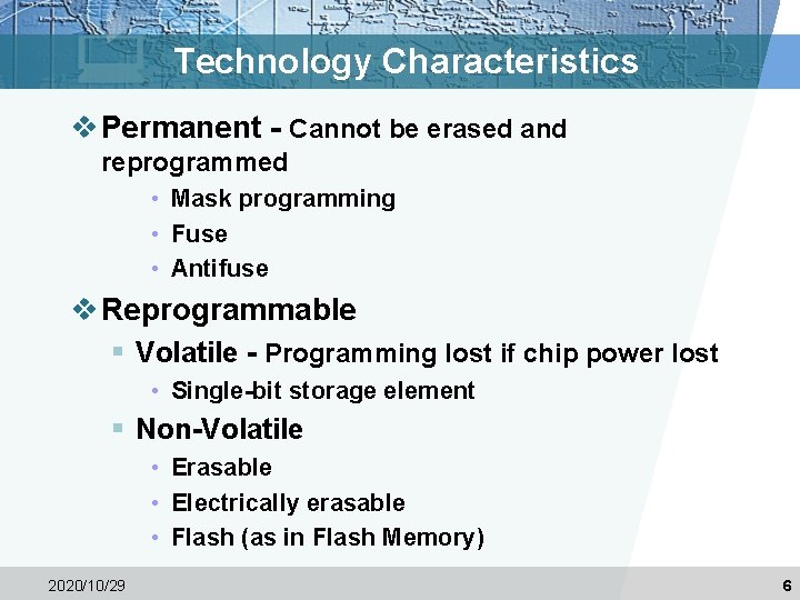
Technology Characteristics v Permanent - Cannot be erased and reprogrammed • Mask programming • Fuse • Antifuse v Reprogrammable § Volatile - Programming lost if chip power lost • Single-bit storage element § Non-Volatile • Erasable • Electrically erasable • Flash (as in Flash Memory) 2020/10/29 6
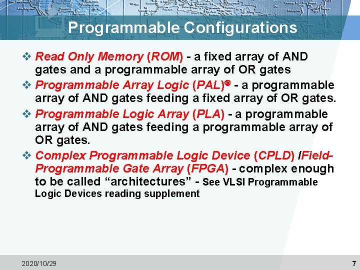
Programmable Configurations v Read Only Memory (ROM) - a fixed array of AND gates and a programmable array of OR gates v Programmable Array Logic (PAL)Ò - a programmable array of AND gates feeding a fixed array of OR gates. v Programmable Logic Array (PLA) - a programmable array of AND gates feeding a programmable array of OR gates. v Complex Programmable Logic Device (CPLD) /Field. Programmable Gate Array (FPGA) - complex enough to be called “architectures” - See VLSI Programmable Logic Devices reading supplement 2020/10/29 7
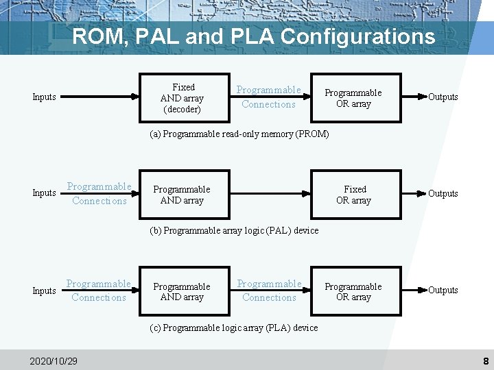
ROM, PAL and PLA Configurations Fixed AND array (decoder) Inputs Programmable Connections Programmable OR array Outputs (a) Programmable read-only memory (PROM) Inputs Programmable Connections Programmable AND array Fixed OR array Outputs Programmable OR array Outputs (b) Programmable array logic (PAL) device Inputs Programmable Connections Programmable AND array Programmable Connections (c) Programmable logic array (PLA) device 2020/10/29 8
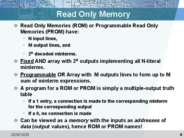
Read Only Memory v Read Only Memories (ROM) or Programmable Read Only Memories (PROM) have: § N input lines, § M output lines, and § 2 N decoded minterms. v Fixed AND array with 2 N outputs implementing all N-literal minterms. v Programmable OR Array with M outputs lines to form up to M sum of minterm expressions. v A program for a ROM or PROM is simply a multiple-output truth table § If a 1 entry, a connection is made to the corresponding minterm for the corresponding output § If a 0, no connection is made v Can be viewed as a memory with the inputs as addresses of data (output values), hence ROM or PROM names! 2020/10/29 9
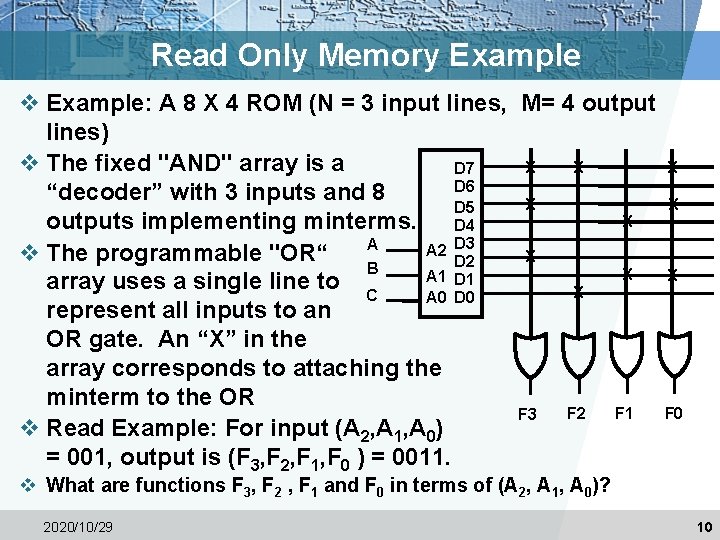
Read Only Memory Example v Example: A 8 X 4 ROM (N = 3 input lines, M= 4 output lines) v The fixed "AND" array is a X X X D 7 D 6 “decoder” with 3 inputs and 8 X X D 5 X outputs implementing minterms. D 4 A A 2 D 3 v The programmable "OR“ X D 2 B X X A 1 D 1 array uses a single line to C X A 0 D 0 represent all inputs to an OR gate. An “X” in the array corresponds to attaching the minterm to the OR F 0 F 2 F 1 F 3 v Read Example: For input (A 2, A 1, A 0) = 001, output is (F 3, F 2, F 1, F 0 ) = 0011. v What are functions F 3, F 2 , F 1 and F 0 in terms of (A 2, A 1, A 0)? 2020/10/29 10
Programmable Array Logic (PAL) v The PAL is the opposite of the ROM, having a programmable set of ANDs combined with fixed ORs. v Disadvantage § ROM guaranteed to implement any M functions of N inputs. PAL may have too few inputs to the OR gates. v Advantages § For given internal complexity, a PAL can have larger N and M § Some PALs have outputs that can be complemented, adding POS functions § No multilevel circuit implementations in ROM (without external connections from output to input). PAL has outputs from OR terms as internal inputs to all AND terms, making implementation of multi-level circuits easier. 2020/10/29 11
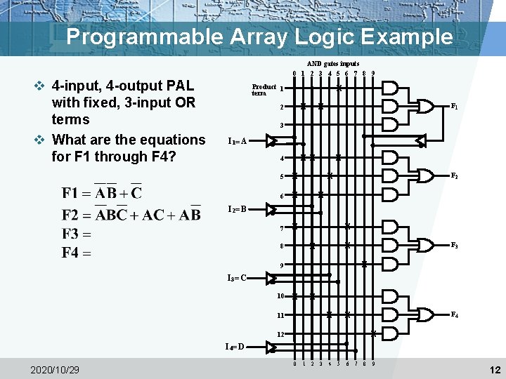
Programmable Array Logic Example AND gates inputs 0 1 2 3 4 5 6 7 8 9 Product 1 term X X 2 X F 1 3 I 1= A XX X 6 F 2 X 5 X 4 X X v 4 -input, 4 -output PAL with fixed, 3 -input OR terms v What are the equations for F 1 through F 4? I 2= B X X 7 8 F 3 X 9 I 3= C X X X 11 X 10 F 4 X 12 I 4= D 2020/10/29 0 1 2 3 4 5 6 7 8 9 12
Programmable Logic Array (PLA) v Compared to a ROM and a PAL, a PLA is the most flexible having a programmable set of ANDs combined with a programmable set of ORs. v Advantages § A PLA can have large N and M permitting implementation of equations that are impractical for a ROM (because of the number of inputs, N, required) § A PLA has all of its product terms connectable to all outputs, overcoming the problem of the limited inputs to the PAL Ors § Some PLAs have outputs that can be complemented, adding POS functions v Disadvantage § Often, the product term count limits the application of a PLA. Two-level multiple-output optimization reduces the number of product terms in an implementation, helping to fit it into a PLA. 2020/10/29 13
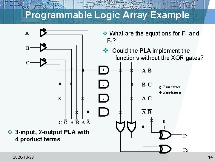
Programmable Logic Array Example A v What are the equations for F 1 and F 2 ? B v Could the PLA implement the functions without the XOR gates? C X X X X AB 2 X BC 3 X AC 1 X X C C B B AA v 3 -input, 2 -output PLA with 4 product terms 4 X X X Fuse intact Fuse blown AB X X 0 1 F 2 2020/10/29 14
Combinational Function Implementation v Implementation techniques: § Decoders and OR gates § Multiplexers (and inverter) § ROMs § PLAs § PALs § Lookup Tables v Can be referred to as structured implementation methods since a specific underlying structure is assumed in each case Chapter 4 15
Decoder and OR Gates v Any combinational circuit with n inputs and m outputs can be implemented with: § an n-to-2 n-line decoder, and § m OR gates (one for each output) v Approach 1: § Find the truth table for the functions § Make a connection to the corresponding OR from the corresponding decoder output wherever a 1 appears in the truth table v Approach 2: § Find all the minterms in the Boolean function § Map the minterms with OR gates. Chapter 4 16
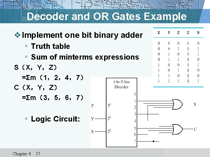
Decoder and OR Gates Example v Implement one bit binary adder § Truth table § Sum of minterms expressions S(X,Y,Z) =Σm(1,2,4,7) C(X,Y,Z) =Σm(3,5,6,7) § Logic Circuit: Chapter 4 17
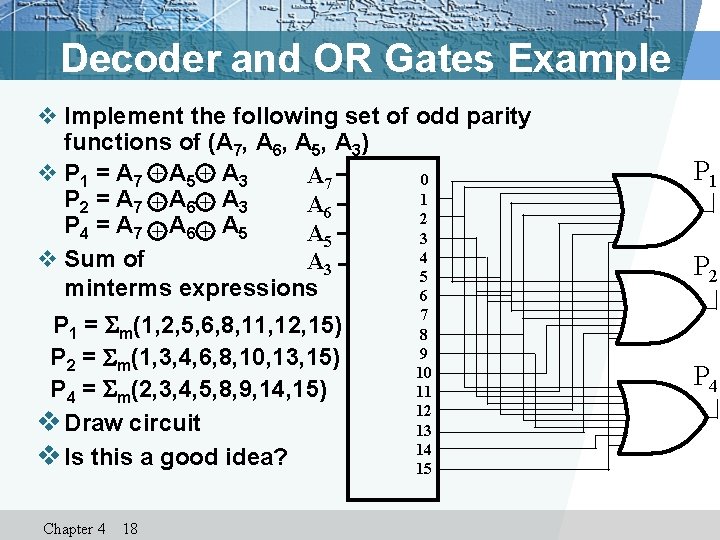
Decoder and OR Gates Example v Implement the following set of odd parity functions of (A 7, A 6, A 5, A 3) + 5 A + 3 v P 1 = A 7 A A 7 0 1 P 2 = A 7 A + 6 A + 3 A 6 2 P 4 = A 7 A + 6 A + 5 A 5 3 4 v Sum of A 3 5 minterms expressions 6 7 P 1 = Sm(1, 2, 5, 6, 8, 11, 12, 15) 8 9 P 2 = Sm(1, 3, 4, 6, 8, 10, 13, 15) 10 P 4 = Sm(2, 3, 4, 5, 8, 9, 14, 15) 11 12 v Draw circuit 13 14 v Is this a good idea? 15 Chapter 4 18 P 1 P 2 P 4
Multiplexer Approach v Implement m functions of n variables with: § Sum-of-minterms expressions § An m-wide 2 n-to-1 -line multiplexer v Design: § Find the truth table for the functions. § In the order they appear in the truth table: • Apply the function input variables to the multiplexer inputs Sn - 1, … , S 0 • Label the outputs of the multiplexer with the output variables § Value-fix the information inputs to the multiplexer using the values from the truth table (for don’t cares, apply either 0 or 1) Chapter 4 19
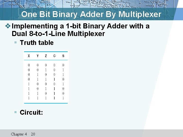
One Bit Binary Adder By Multiplexer v Implementing a 1 -bit Binary Adder with a Dual 8 -to-1 -Line Multiplexer § Truth table § Circuit: Chapter 4 20
Not Enough Control Pole for Multiplexer v Implement a multiplexer of n+1 variables and m functions with the following devices: § M-bit width 2 n -to-1 Multiplexer § One invertor v Design: § Derive the truth table § Using X+X law, the truth table is separated into two parts based on the first n variable § Use the variable as another input for the multiplexer, now the input combination is (0, 1, X, X) Chapter 4 21
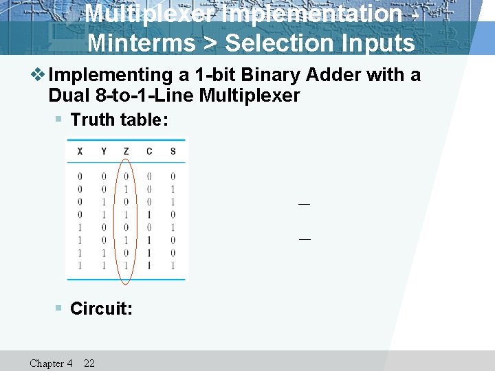
Multiplexer Implementation - Minterms > Selection Inputs v Implementing a 1 -bit Binary Adder with a Dual 8 -to-1 -Line Multiplexer § Truth table: § Circuit: Chapter 4 22
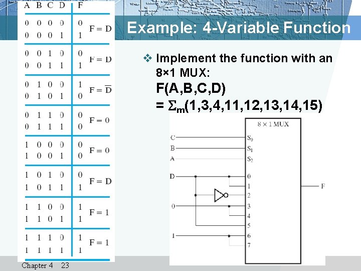
Example: 4 -Variable Function v Implement the function with an 8× 1 MUX: F(A, B, C, D) = Sm(1, 3, 4, 11, 12, 13, 14, 15) Chapter 4 23
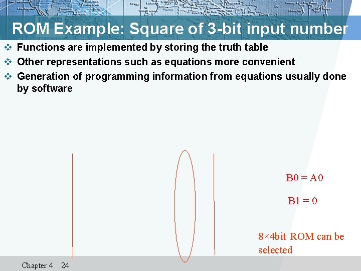
ROM Example: Square of 3 -bit input number v Functions are implemented by storing the truth table v Other representations such as equations more convenient v Generation of programming information from equations usually done by software B 0 = A 0 B 1 = 0 8× 4 bit ROM can be selected Chapter 4 24
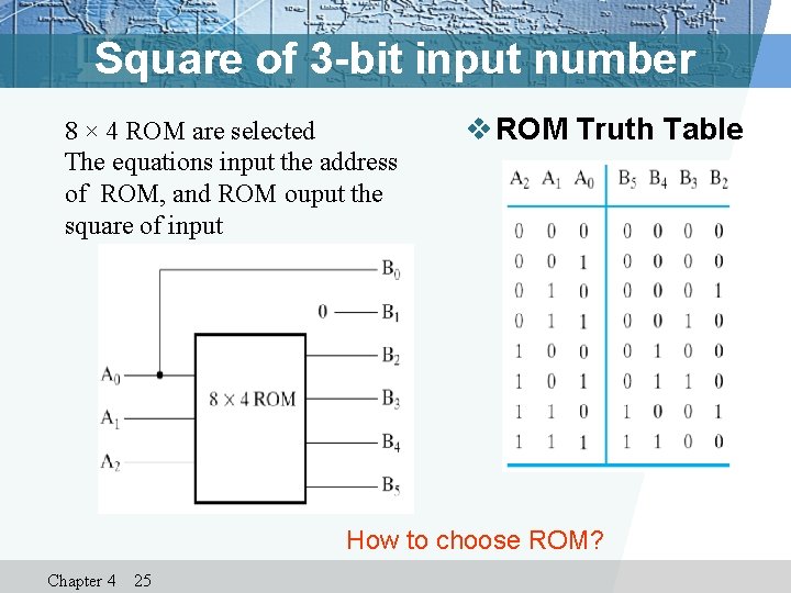
Square of 3 -bit input number 8 × 4 ROM are selected The equations input the address of ROM, and ROM ouput the square of input v ROM Truth Table How to choose ROM? Chapter 4 25
Lookup Tables v Lookup tables are used for implementing logic in Field-Programmable Gate Arrays (FPGAs) and Complex Logic Devices (CPLDs) v Lookup tables are typically small, often with four inputs, one output, and 16 entries v Since lookup tables store truth tables, it is possible to implement any 4 -input function v Thus, the design problem is how to optimally decompose a set of given functions into a set of 4 -input two- level functions. v We will illustrate this by a manual attempt Chapter 4 26
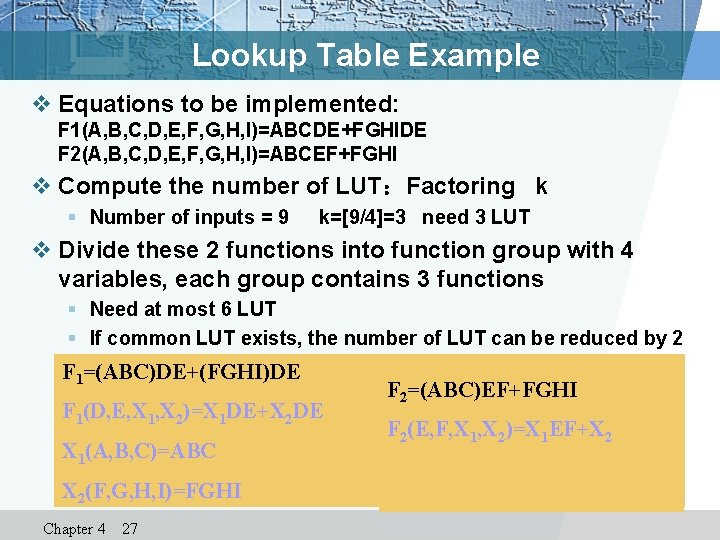
Lookup Table Example v Equations to be implemented: F 1(A, B, C, D, E, F, G, H, I)=ABCDE+FGHIDE F 2(A, B, C, D, E, F, G, H, I)=ABCEF+FGHI v Compute the number of LUT:Factoring k § Number of inputs = 9 k=[9/4]=3 need 3 LUT v Divide these 2 functions into function group with 4 variables, each group contains 3 functions § Need at most 6 LUT § If common LUT exists, the number of LUT can be reduced by 2 F 1=(ABC)DE+(FGHI)DE F 1(D, E, X 1, X 2)=X 1 DE+X 2 DE X 1(A, B, C)=ABC X 2(F, G, H, I)=FGHI Chapter 4 27 F 2=(ABC)EF+FGHI F 2(E, F, X 1, X 2)=X 1 EF+X 2
Programmable Logic Array v The set of functions to be implemented must fit the available number of product terms v The number of literals per term is less important in fitting v The best approach to fitting is multiple-output, twolevel optimization (which has not been discussed) v Since output inversion is available, terms can implement by either a function or its complement v For small circuits, K-maps can be used to visualize product term sharing and use of complements v For larger circuits, software is used to do the optimization including use of complemented functions Chapter 4 28
Programmable Logic Array Example v lists the product term numbers v Specifies the required paths between inputs and AND gates v Specifies the paths between the AND and OR gates v For each output variable, we may have a T or C for controlling the output exclusive-OR gate Chapter 4 29 Build the programming table
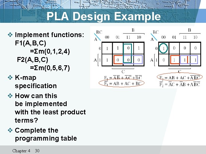
PLA Design Example v Implement functions: F 1(A, B, C) =Σm(0, 1, 2, 4) F 2(A, B, C) =Σm(0, 5, 6, 7) v K-map specification v How can this be implemented with the least product terms? v Complete the programming table Chapter 4 30
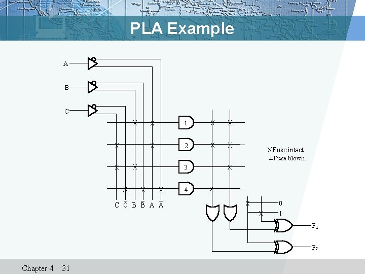
PLA Example A B C X X X 1 X X X 2 X X XFuse intact +Fuse blown X X 3 X X C C B B A A 4 X X X 0 1 F 2 Chapter 4 31
Programmable Array Logic v Different from ROM and PLA, there is no sharing of AND gates v Design requires fitting functions within the limited number of ANDs per OR gate v Single function optimization is the first step to fitting v If the number of product terms in a function is greater than the number of ANDs per OR gate, then factoring is necessary Chapter 4 32
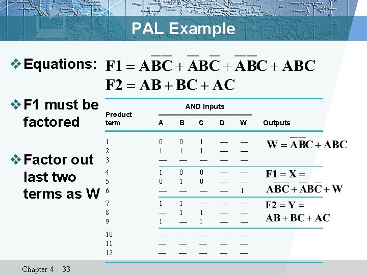
PAL Example v Equations: v F 1 must be factored v Factor out last two terms as W Chapter 4 33 AND Inputs Product term A B C D W 1 2 3 0 1 — 1 1 — — — — 4 5 6 1 0 — 0 1 — 0 0 — — — 1 7 8 9 1 — 1 1 1 — — — — 10 11 12 — — — — Outputs
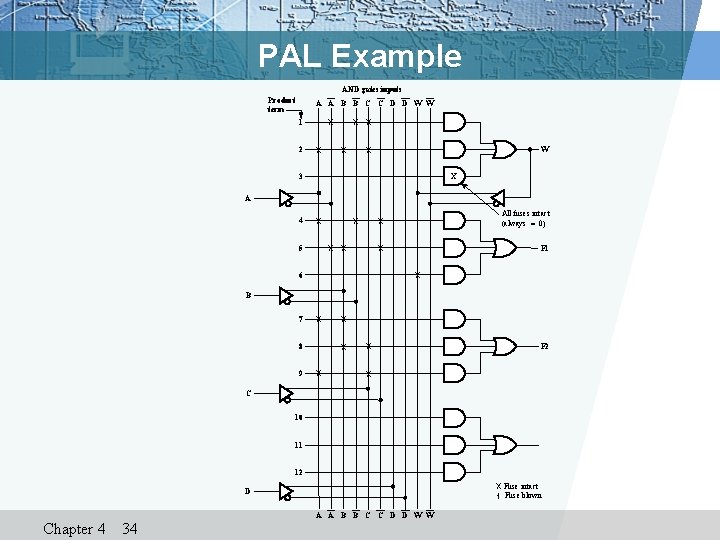
PAL Example AND gates inputs Product term A A B B C C D D W W 1 2 X X X W X 3 X A 4 X X 5 X All fuses intact (always = 0) X F 1 X 6 B 7 X 8 9 X X F 2 X C 10 11 12 X Fuse intact 1 Fuse blown D Chapter 4 34 A A B B C C D D W W
Assignment Reading: pp. 319 --329 Problem Assignment: 6 -12, 6 -20 2020/10/29 35
- Slides: 35