Logic and Computer Design Fundamentals Lecture 12 Design

- Slides: 30

Logic and Computer Design Fundamentals Lecture 12 – Design Procedure Charles Kime & Thomas Kaminski © 2004 Pearson Education, Inc. Terms of Use (Hyperlinks are active in View Show mode)

Outline § Design Procedure • • Specification Formulation Optimization Technology Mapping § NAND gates § NOR gates • Verification Chapter 3 - Part 1 2

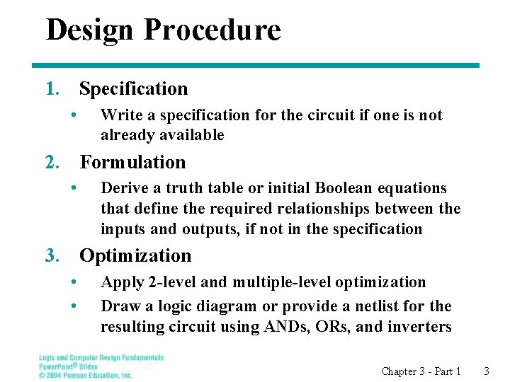
Design Procedure 1. Specification • Write a specification for the circuit if one is not already available 2. Formulation • Derive a truth table or initial Boolean equations that define the required relationships between the inputs and outputs, if not in the specification 3. Optimization • • Apply 2 -level and multiple-level optimization Draw a logic diagram or provide a netlist for the resulting circuit using ANDs, ORs, and inverters Chapter 3 - Part 1 3

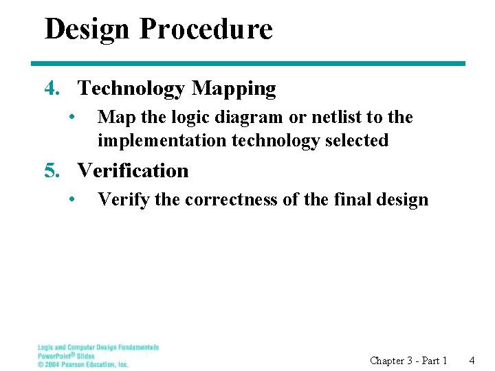
Design Procedure 4. Technology Mapping • Map the logic diagram or netlist to the implementation technology selected 5. Verification • Verify the correctness of the final design Chapter 3 - Part 1 4

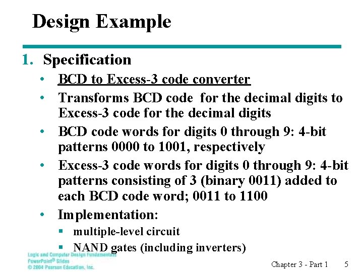
Design Example 1. Specification • BCD to Excess-3 code converter • Transforms BCD code for the decimal digits to Excess-3 code for the decimal digits • BCD code words for digits 0 through 9: 4 -bit patterns 0000 to 1001, respectively • Excess-3 code words for digits 0 through 9: 4 -bit patterns consisting of 3 (binary 0011) added to each BCD code word; 0011 to 1100 • Implementation: § multiple-level circuit § NAND gates (including inverters) Chapter 3 - Part 1 5

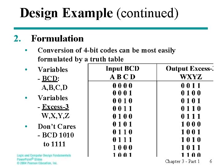
Design Example (continued) 2. Formulation • • Conversion of 4 -bit codes can be most easily formulated by a truth table Variables - BCD: A, B, C, D Variables - Excess-3 W, X, Y, Z Don’t Cares - BCD 1010 to 1111 Chapter 3 - Part 1 6

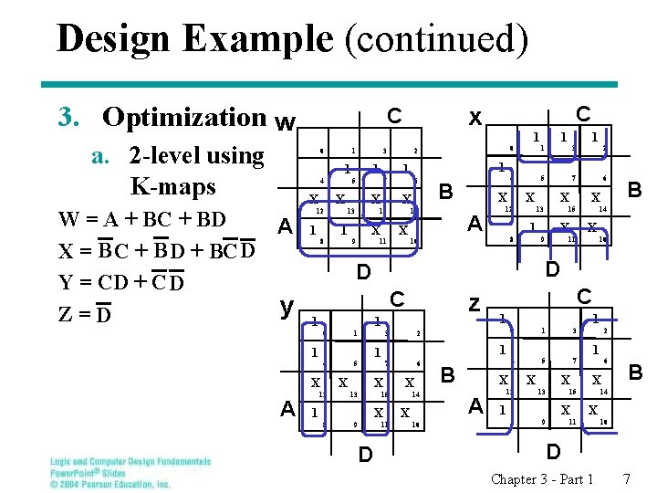
Design Example (continued) 3. Optimization w a. 2 -level using K-maps 0 1 3 1 4 X W = A + BC + BD A X = B C + B D + BC D Y = CD + CD y Z=D 1 12 1 X 13 1 8 X X 9 B 14 3 2 4 5 7 6 X X 12 A X 11 z 1 3 X 7 X 12 13 8 9 1 X 9 B 14 X 11 10 6 X 15 X 11 D C 1 1 0 1 3 4 5 7 1 5 X 15 1 2 1 4 X D 1 1 X 13 8 10 C 1 1 1 D 0 A 6 15 1 0 1 7 X 1 2 1 5 C x C 14 X 10 B 1 X A 2 X X 12 13 8 9 1 6 X 15 X B 14 X 11 10 D Chapter 3 - Part 1 7

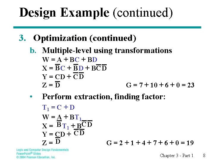
Design Example (continued) 3. Optimization (continued) b. Multiple-level using transformations W = A + BC + BD X = B C + B D + BCD Y = CD + C D Z=D • G = 7 + 10 + 6 + 0 = 23 Perform extraction, finding factor: T 1 = C + D W = A + BT 1 X = B T 1 + BCD Y = CD + C D Z= D G = 2 + 1 + 4 + 7 + 6 + 0 = 19 Chapter 3 - Part 1 8

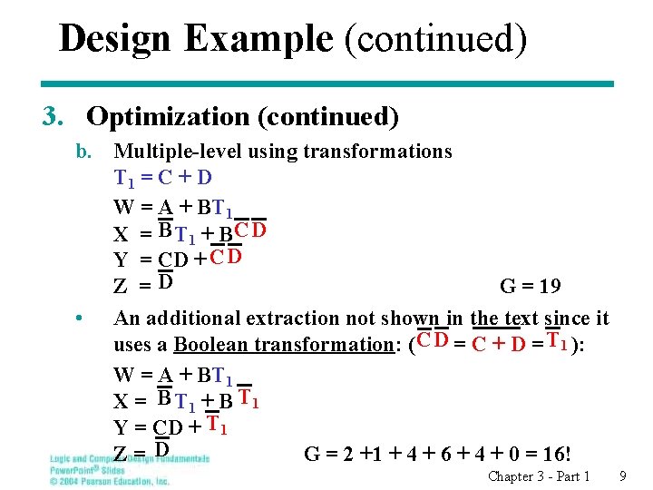
Design Example (continued) 3. Optimization (continued) b. Multiple-level using transformations T 1 = C + D W = A + BT 1 X = B T 1 + BCD Y = CD + C D Z =D G = 19 • An additional extraction not shown in the text since it uses a Boolean transformation: ( CD = C + D = T 1 ): W = A + BT 1 X = B T 1 + B T 1 Y = CD + T 1 Z= D G = 2 +1 + 4 + 6 + 4 + 0 = 16! Chapter 3 - Part 1 9

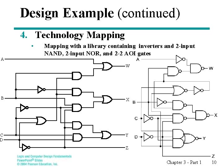
Design Example (continued) 4. Technology Mapping • Mapping with a library containing inverters and 2 -input NAND, 2 -input NOR, and 2 -2 AOI gates A W B X C D Y Z Chapter 3 - Part 1 10

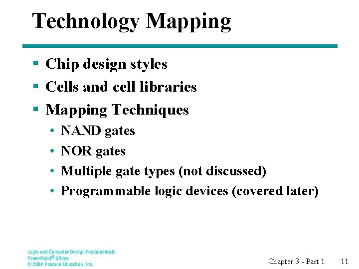
Technology Mapping § Chip design styles § Cells and cell libraries § Mapping Techniques • • NAND gates NOR gates Multiple gate types (not discussed) Programmable logic devices (covered later) Chapter 3 - Part 1 11

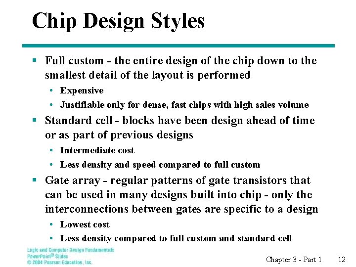
Chip Design Styles § Full custom - the entire design of the chip down to the smallest detail of the layout is performed • Expensive • Justifiable only for dense, fast chips with high sales volume § Standard cell - blocks have been design ahead of time or as part of previous designs • Intermediate cost • Less density and speed compared to full custom § Gate array - regular patterns of gate transistors that can be used in many designs built into chip - only the interconnections between gates are specific to a design • Lowest cost • Less density compared to full custom and standard cell Chapter 3 - Part 1 12

Cell Libraries § Cell - a pre-designed primitive block § Cell library - a collection of cells available for design using a particular implementation technology § Cell characterization - a detailed specification of a cell for use by a designer - often based on actual cell design and fabrication and measured values § Cells are used for gate array, standard cell, and in some cases, full custom chip design Chapter 3 - Part 1 13

Typical Cell Characterization Components § Schematic or logic diagram § Area of cell • Often normalized to the area of a common, small cell such as an inverter § Input loading (in standard loads) presented to outputs driving each of the inputs § Delays from each input to each output § One or more cell templates for technology mapping § One or more hardware description language models § If automatic layout is to be used: • Physical layout of the cell circuit • A floorplan layout providing the location of inputs, outputs, power and ground connections on the cell Chapter 3 - Part 1 14

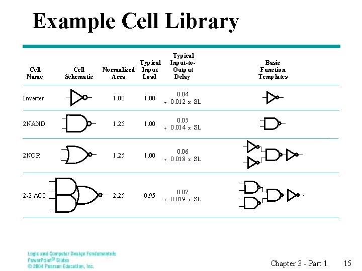
Example Cell Library Typical Input-to. Output Delay Normalized Area Typical Input Load Inverter 1. 00 0. 04 + 0. 012 x SL 2 NAND 1. 25 1. 00 0. 05 + 0. 014 x SL 2 NOR 1. 25 1. 00 0. 06 + 0. 018 x SL 2 -2 AOI 2. 25 0. 95 0. 07 + 0. 019 x SL Cell Name Cell Schematic Basic Function Templates Chapter 3 - Part 1 15

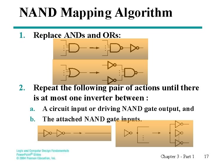
Mapping to NAND gates § Assumptions: • Gate loading and delay are ignored • Cell library contains an inverter and n-input NAND gates, n = 2, 3, … • An AND, OR, inverter schematic for the circuit is available § The mapping is accomplished by: • Replacing AND and OR symbols, • Pushing inverters through circuit fan-out points, and • Canceling inverter pairs Chapter 3 - Part 1 16

NAND Mapping Algorithm 1. Replace ANDs and ORs: . . . 2. Repeat the following pair of actions until there is at most one inverter between : a. A circuit input or driving NAND gate output, and b. The attached NAND gate inputs. Chapter 3 - Part 1 17

NAND Mapping Example Chapter 3 - Part 1 18

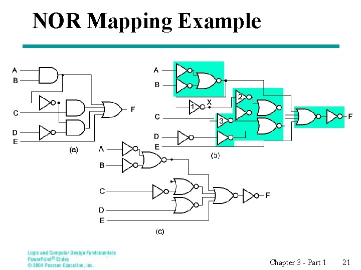
Mapping to NOR gates § Assumptions: • Gate loading and delay are ignored • Cell library contains an inverter and n-input NOR gates, n = 2, 3, … • An AND, OR, inverter schematic for the circuit is available § The mapping is accomplished by: • Replacing AND and OR symbols, • Pushing inverters through circuit fan-out points, and • Canceling inverter pairs Chapter 3 - Part 1 19

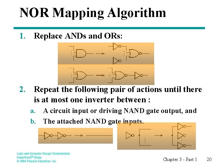
NOR Mapping Algorithm 1. Replace ANDs and ORs: 2. Repeat the following pair of actions until there is at most one inverter between : a. A circuit input or driving NAND gate output, and b. The attached NAND gate inputs. Chapter 3 - Part 1 20

NOR Mapping Example Chapter 3 - Part 1 21

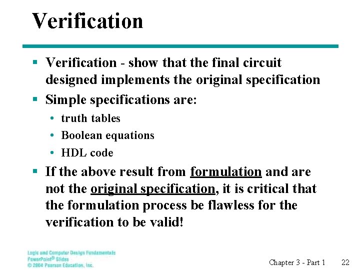
Verification § Verification - show that the final circuit designed implements the original specification § Simple specifications are: • truth tables • Boolean equations • HDL code § If the above result from formulation and are not the original specification, it is critical that the formulation process be flawless for the verification to be valid! Chapter 3 - Part 1 22

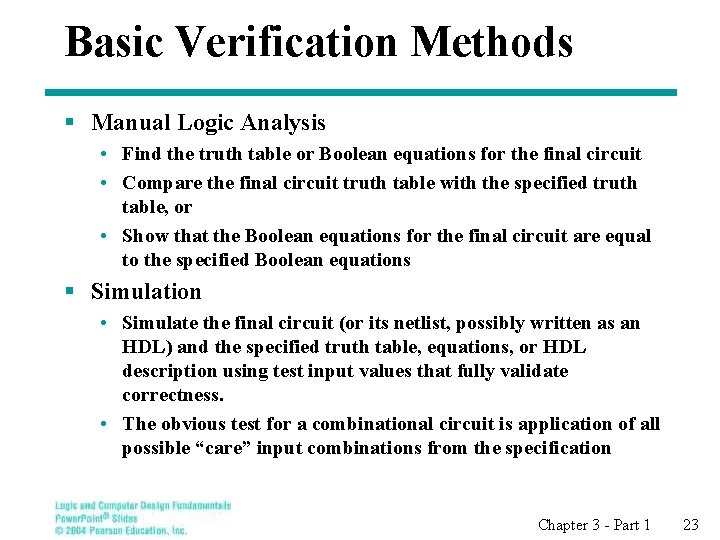
Basic Verification Methods § Manual Logic Analysis • Find the truth table or Boolean equations for the final circuit • Compare the final circuit truth table with the specified truth table, or • Show that the Boolean equations for the final circuit are equal to the specified Boolean equations § Simulation • Simulate the final circuit (or its netlist, possibly written as an HDL) and the specified truth table, equations, or HDL description using test input values that fully validate correctness. • The obvious test for a combinational circuit is application of all possible “care” input combinations from the specification Chapter 3 - Part 1 23

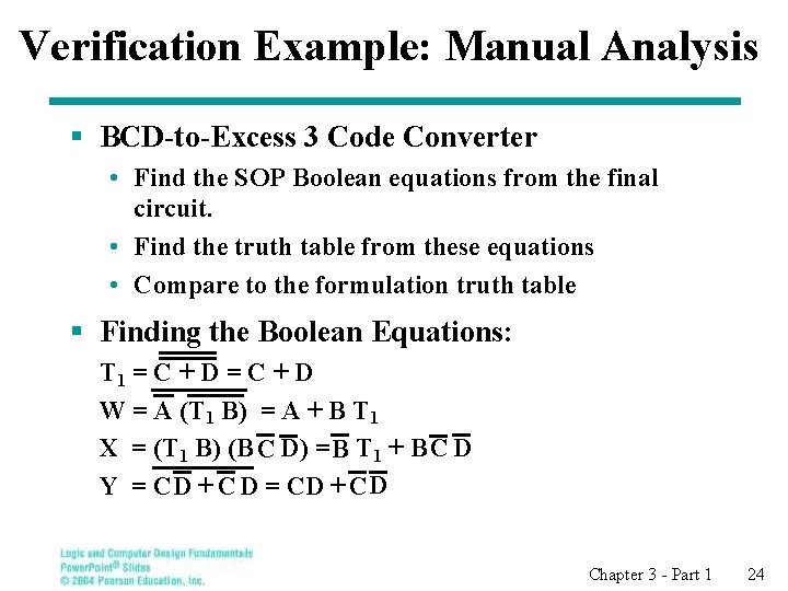
Verification Example: Manual Analysis § BCD-to-Excess 3 Code Converter • Find the SOP Boolean equations from the final circuit. • Find the truth table from these equations • Compare to the formulation truth table § Finding the Boolean Equations: T 1 = C + D W = A (T 1 B) = A + B T 1 X = (T 1 B) (B C D) = B T 1 + B C D Y = C D + C D = CD + CD Chapter 3 - Part 1 24

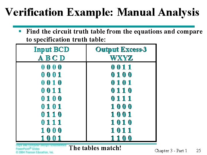
Verification Example: Manual Analysis § Find the circuit truth table from the equations and compare to specification truth table: Input BCD ABCD 0000 0001 0010 0011 0100 0101 0110 0111 1000 1001 Output Excess-3 WXYZ 0011 0100 0101 0110 0111 1000 1001 1010 1011 1100 The tables match! Chapter 3 - Part 1 25

Verification Example: Simulation § Simulation procedure: • Use a schematic editor or text editor to enter a gate level representation of the final circuit • Use a waveform editor or text editor to enter a test consisting of a sequence of input combinations to be applied to the circuit § This test should guarantee the correctness of the circuit if the simulated responses to it are correct § Short of applying all possible “care” input combinations, generation of such a test can be difficult Chapter 3 - Part 1 26

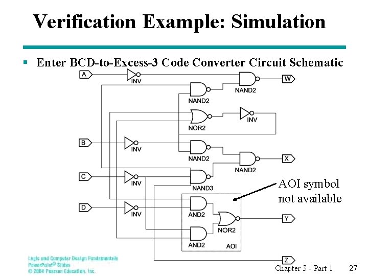
Verification Example: Simulation § Enter BCD-to-Excess-3 Code Converter Circuit Schematic AOI symbol not available Chapter 3 - Part 1 27

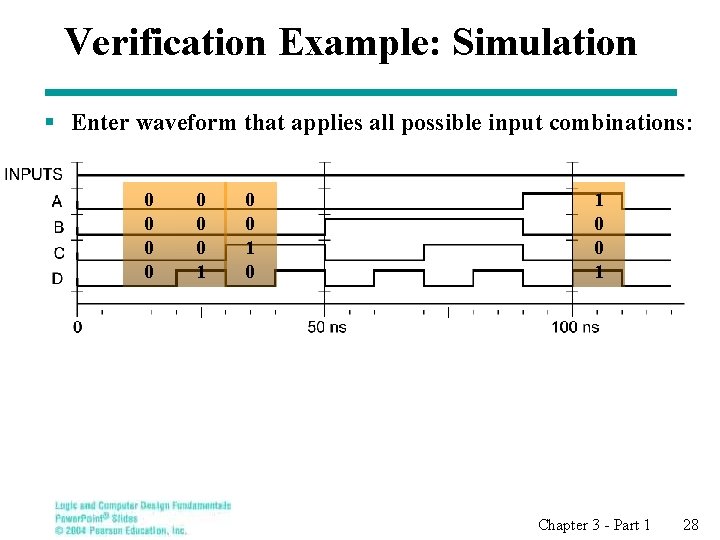
Verification Example: Simulation § Enter waveform that applies all possible input combinations: 0 0 0 0 1 Chapter 3 - Part 1 28

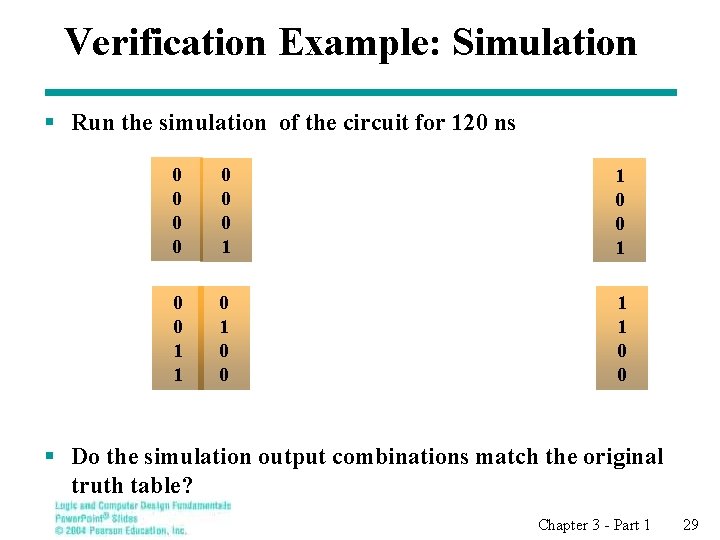
Verification Example: Simulation § Run the simulation of the circuit for 120 ns 0 0 0 0 1 1 0 0 1 1 0 0 § Do the simulation output combinations match the original truth table? Chapter 3 - Part 1 29

Summary § Design Procedure • • Specification Formulation Optimization Technology Mapping § NAND gates § NOR gates • Verification Chapter 3 - Part 1 30