Logic and Computer Design Fundamentals Chapter 7 Registers


- Slides: 49

Logic and Computer Design Fundamentals Chapter 7 – Registers and Register Transfers Haifeng Liu haifengliu@zju. edu. cn College of Computer Science and Technology, Zhejiang University

Overview § Registers and load enable § Register transfer operations § Multiplexer and bus-based transfers for multiple registers § Shift registers § Counters Chapter 7 - 2

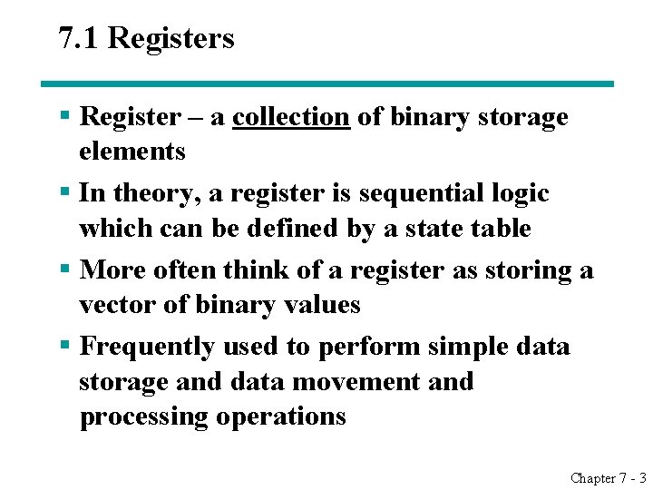
7. 1 Registers § Register – a collection of binary storage elements § In theory, a register is sequential logic which can be defined by a state table § More often think of a register as storing a vector of binary values § Frequently used to perform simple data storage and data movement and processing operations Chapter 7 - 3

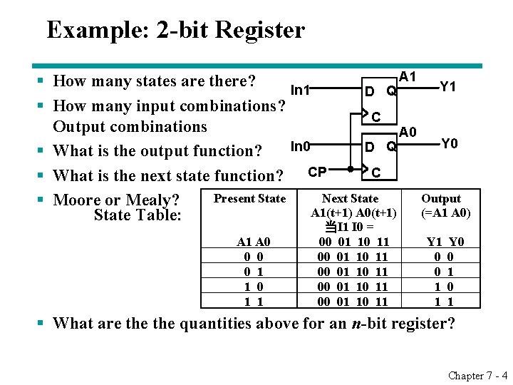
Example: 2 -bit Register A 1 § How many states are there? Y 1 In 1 D Q § How many input combinations? C Output combinations A 0 Y 0 In 0 D Q § What is the output function? C § What is the next state function? CP Present State Next State Output § Moore or Mealy? A 1(t+1) A 0(t+1) (=A 1 A 0) State Table: A 1 A 0 0 1 1 当I 1 I 0 = 00 01 10 11 00 01 10 11 Y 0 0 1 1 0 1 1 § What are the quantities above for an n-bit register? Chapter 7 - 4

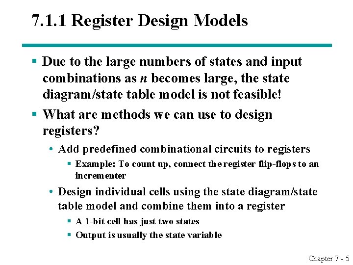
7. 1. 1 Register Design Models § Due to the large numbers of states and input combinations as n becomes large, the state diagram/state table model is not feasible! § What are methods we can use to design registers? • Add predefined combinational circuits to registers § Example: To count up, connect the register flip-flops to an incrementer • Design individual cells using the state diagram/state table model and combine them into a register § A 1 -bit cell has just two states § Output is usually the state variable Chapter 7 - 5

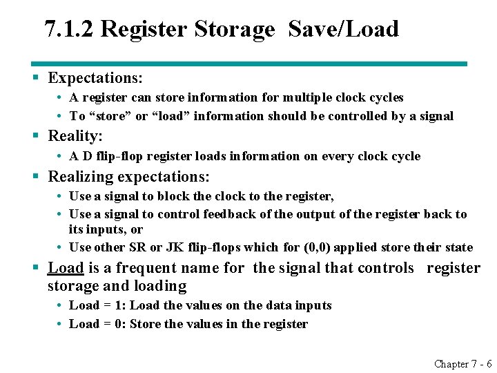
7. 1. 2 Register Storage Save/Load § Expectations: • A register can store information for multiple clock cycles • To “store” or “load” information should be controlled by a signal § Reality: • A D flip-flop register loads information on every clock cycle § Realizing expectations: • Use a signal to block the clock to the register, • Use a signal to control feedback of the output of the register back to its inputs, or • Use other SR or JK flip-flops which for (0, 0) applied store their state § Load is a frequent name for the signal that controls register storage and loading • Load = 1: Load the values on the data inputs • Load = 0: Store the values in the register Chapter 7 - 6

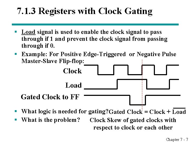
7. 1. 3 Registers with Clock Gating § Load signal is used to enable the clock signal to pass through if 1 and prevent the clock signal from passing through if 0. § Example: For Positive Edge-Triggered or Negative Pulse Master-Slave Flip-flop: Clock Load Gated Clock to FF § What logic is needed for gating? Gated Clock = Clock + Load § What is the problem? Clock Skew of gated clocks with respect to clock or each other Chapter 7 - 7

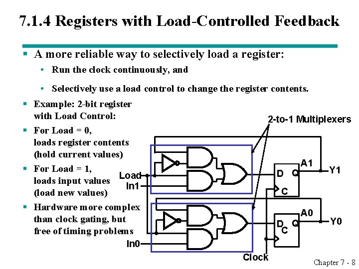
7. 1. 4 Registers with Load-Controlled Feedback § A more reliable way to selectively load a register: • Run the clock continuously, and § § • Selectively use a load control to change the register contents. Example: 2 -bit register with Load Control: 2 -to-1 Multiplexers For Load = 0, loads register contents (hold current values) A 1 For Load = 1, Y 1 D Q Load loads input values In 1 C (load new values) Hardware more complex A 0 than clock gating, but Y 0 D Q C free of timing problems In 0 Clock Chapter 7 - 8

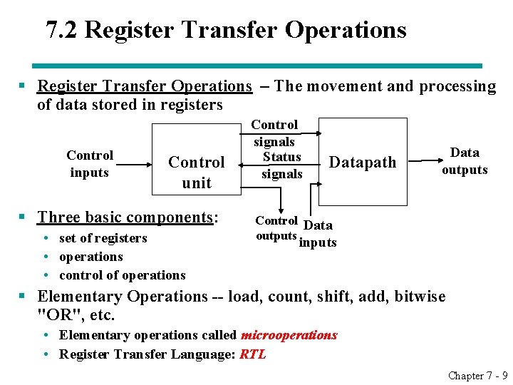
7. 2 Register Transfer Operations § Register Transfer Operations – The movement and processing of data stored in registers Control inputs Control unit § Three basic components: • set of registers • operations • control of operations Control signals Status signals Datapath Data outputs Control Data outputs inputs § Elementary Operations -- load, count, shift, add, bitwise "OR", etc. • Elementary operations called microoperations • Register Transfer Language: RTL Chapter 7 - 9

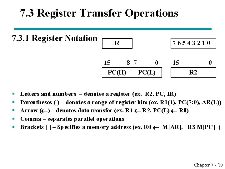
7. 3 Register Transfer Operations 7. 3. 1 Register Notation R 7 6 5 4 3 2 1 0 15 8 7 0 15 0 PC(H) PC(L) R 2 § § § Letters and numbers – denotes a register (ex. R 2, PC, IR) Parentheses ( ) – denotes a range of register bits (ex. R 1(1), PC(7: 0), AR(L)) Arrow ( ) – denotes data transfer (ex. R 1 R 2, PC(L) R 0) Comma – separates parallel operations Brackets [ ] – Specifies a memory address (ex. R 0 M[AR], R 3 M[PC] ) Chapter 7 - 10

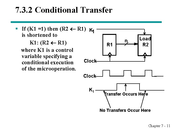
7. 3. 2 Conditional Transfer § If (K 1 =1) then (R 2 R 1) K 1 is shortened to K 1: (R 2 R 1) where K 1 is a control variable specifying a Clock conditional execution of the microoperation. R 1 n Load R 2 Clock K 1 Transfer Occurs Here No Transfers Occur Here Chapter 7 - 11

7. 4 Comparison of Hardware Description Language Chapter 7 - 12

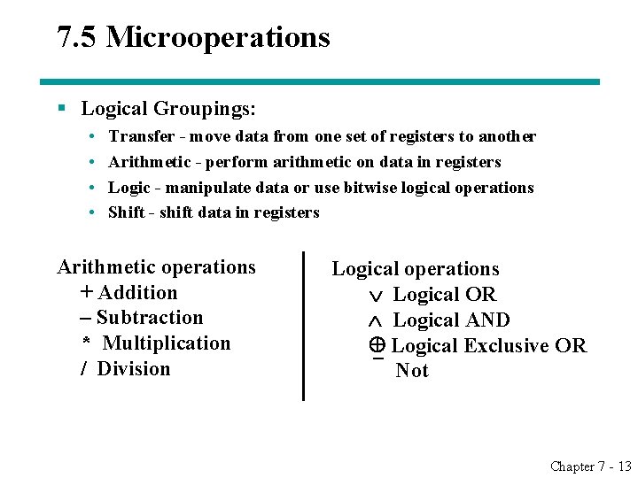
7. 5 Microoperations § Logical Groupings: • • Transfer - move data from one set of registers to another Arithmetic - perform arithmetic on data in registers Logic - manipulate data or use bitwise logical operations Shift - shift data in registers Arithmetic operations + Addition – Subtraction * Multiplication / Division Logical operations Logical OR Logical AND Logical Exclusive OR Not Chapter 7 - 13

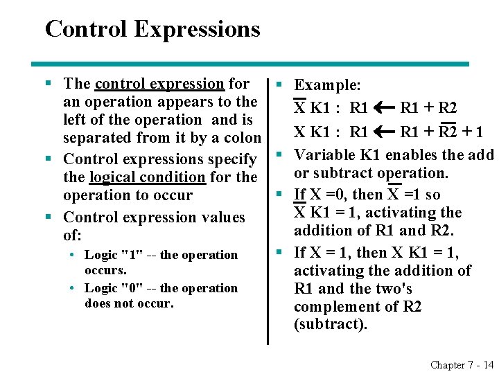
Control Expressions § The control expression for § Example: an operation appears to the X K 1 : R 1 + R 2 left of the operation and is X K 1 : R 1 + R 2 + 1 separated from it by a colon § Control expressions specify § Variable K 1 enables the add or subtract operation. the logical condition for the § If X =0, then X =1 so operation to occur X K 1 = 1, activating the § Control expression values addition of R 1 and R 2. of: § If X = 1, then X K 1 = 1, • Logic "1" -- the operation occurs. activating the addition of • Logic "0" -- the operation R 1 and the two's does not occur. complement of R 2 (subtract). Chapter 7 - 14

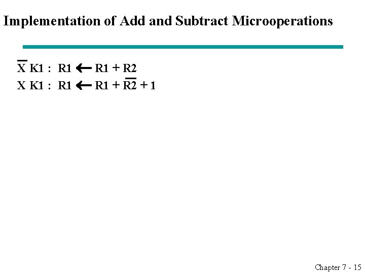
Implementation of Add and Subtract Microoperations X K 1 : R 1 + R 2 + 1 Chapter 7 - 15

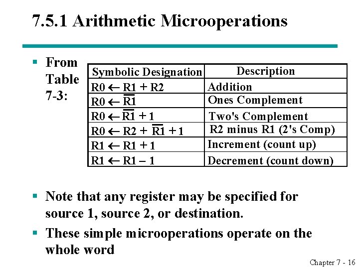
7. 5. 1 Arithmetic Microoperations § From Description Symbolic Designation Table Addition R 0 R 1 + R 2 7 -3: Ones Complement R 0 R 1 + 1 R 0 R 2 + R 1 + 1 R 1 – 1 Two's Complement R 2 minus R 1 (2's Comp) Increment (count up) Decrement (count down) § Note that any register may be specified for source 1, source 2, or destination. § These simple microoperations operate on the whole word Chapter 7 - 16

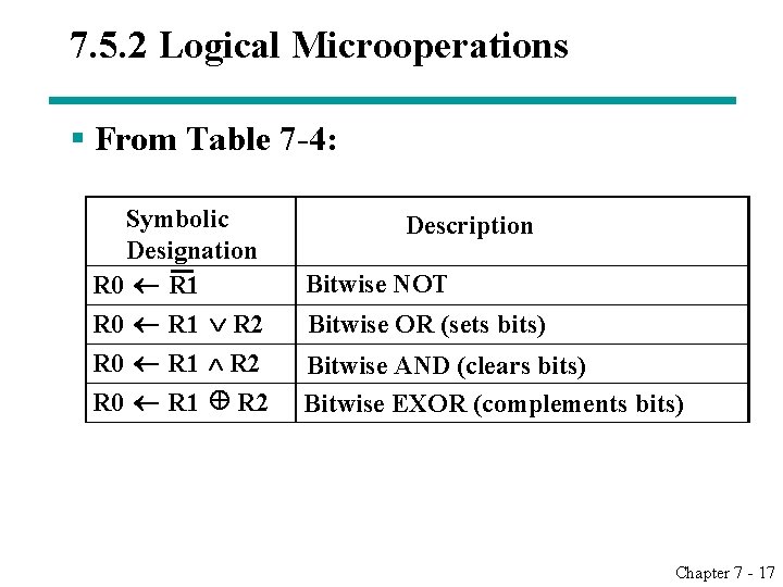
7. 5. 2 Logical Microoperations § From Table 7 -4: Symbolic Description Designation Bitwise NOT R 0 R 1 R 2 Bitwise OR (sets bits) R 0 R 1 R 2 Bitwise AND (clears bits) R 0 R 1 R 2 Bitwise EXOR (complements bits) Chapter 7 - 17

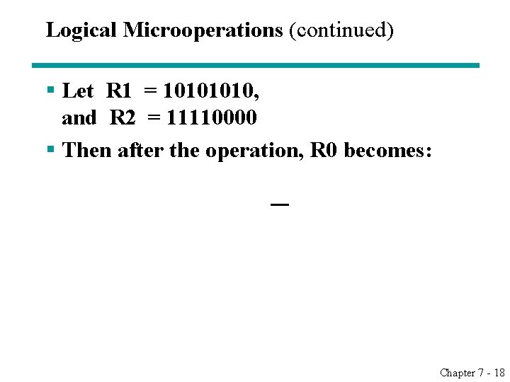
Logical Microoperations (continued) § Let R 1 = 1010, and R 2 = 11110000 § Then after the operation, R 0 becomes: Chapter 7 - 18

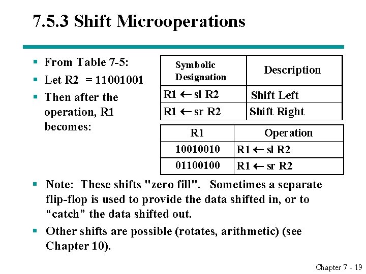
7. 5. 3 Shift Microoperations § From Table 7 -5: § Let R 2 = 11001001 § Then after the operation, R 1 becomes: Symbolic Designation R 1 sl R 2 R 1 sr R 2 Description Shift Left Shift Right R 1 10010010 01100100 Operation R 1 sl R 2 R 1 sr R 2 § Note: These shifts "zero fill". Sometimes a separate flip-flop is used to provide the data shifted in, or to “catch” the data shifted out. § Other shifts are possible (rotates, arithmetic) (see Chapter 10). Chapter 7 - 19

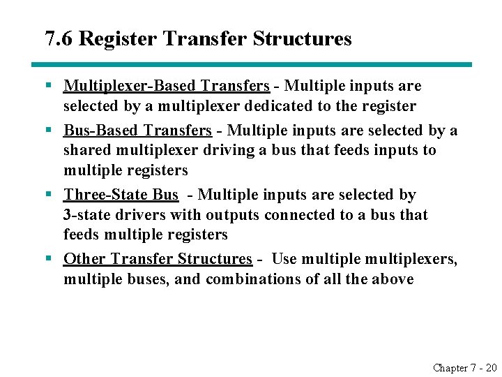
7. 6 Register Transfer Structures § Multiplexer-Based Transfers - Multiple inputs are selected by a multiplexer dedicated to the register § Bus-Based Transfers - Multiple inputs are selected by a shared multiplexer driving a bus that feeds inputs to multiple registers § Three-State Bus - Multiple inputs are selected by 3 -state drivers with outputs connected to a bus that feeds multiple registers § Other Transfer Structures - Use multiplexers, multiple buses, and combinations of all the above Chapter 7 - 20

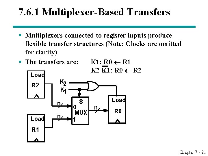
7. 6. 1 Multiplexer-Based Transfers § Multiplexers connected to register inputs produce flexible transfer structures (Note: Clocks are omitted for clarity) § The transfers are: K 1: R 0 R 1 K 2 K 1: R 0 R 2 Load R 2 K 1 n Load n S 0 MUX 1 Load n R 0 R 1 Chapter 7 - 21

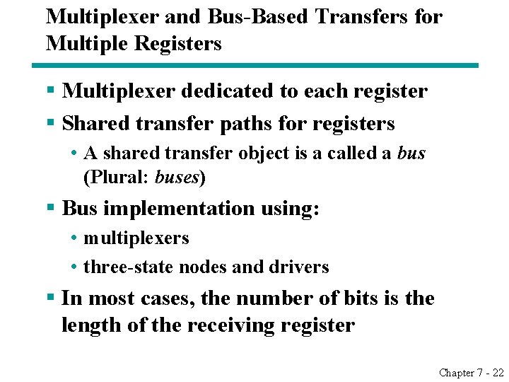
Multiplexer and Bus-Based Transfers for Multiple Registers § Multiplexer dedicated to each register § Shared transfer paths for registers • A shared transfer object is a called a bus (Plural: buses) § Bus implementation using: • multiplexers • three-state nodes and drivers § In most cases, the number of bits is the length of the receiving register Chapter 7 - 22

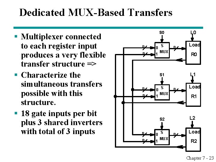
Dedicated MUX-Based Transfers § Multiplexer connected to each register input produces a very flexible transfer structure => § Characterize the simultaneous transfers possible with this structure. § 18 gate inputs per bit plus 3 shared inverters with total of 3 inputs L 0 S 0 n 1 S n MUX R 0 L 1 S 1 n 0 n 1 S n MUX 0 n 1 S MUX Load R 1 L 2 S 2 n Load R 2 Chapter 7 - 23

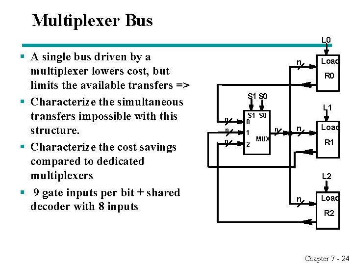
Multiplexer Bus L 0 § A single bus driven by a multiplexer lowers cost, but limits the available transfers => § Characterize the simultaneous transfers impossible with this structure. § Characterize the cost savings compared to dedicated multiplexers § 9 gate inputs per bit + shared decoder with 8 inputs n Load R 0 S 1 S 0 n S 1 S 0 0 n 1 n 2 L 1 n n MUX Load R 1 L 2 n Load R 2 Chapter 7 - 24

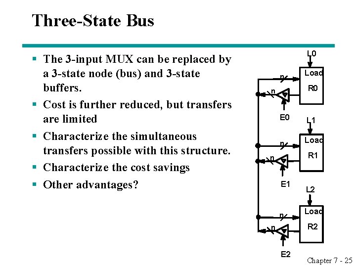
Three-State Bus § The 3 -input MUX can be replaced by a 3 -state node (bus) and 3 -state buffers. § Cost is further reduced, but transfers are limited § Characterize the simultaneous transfers possible with this structure. § Characterize the cost savings § Other advantages? L 0 n Load R 0 n E 0 L 1 n Load R 1 n E 1 n L 2 Load R 2 n E 2 Chapter 7 - 25

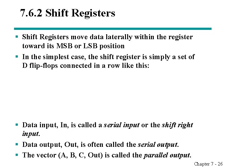
7. 6. 2 Shift Registers § Shift Registers move data laterally within the register toward its MSB or LSB position § In the simplest case, the shift register is simply a set of D flip-flops connected in a row like this: § Data input, In, is called a serial input or the shift right input. § Data output, Out, is often called the serial output. § The vector (A, B, C, Out) is called the parallel output. Chapter 7 - 26

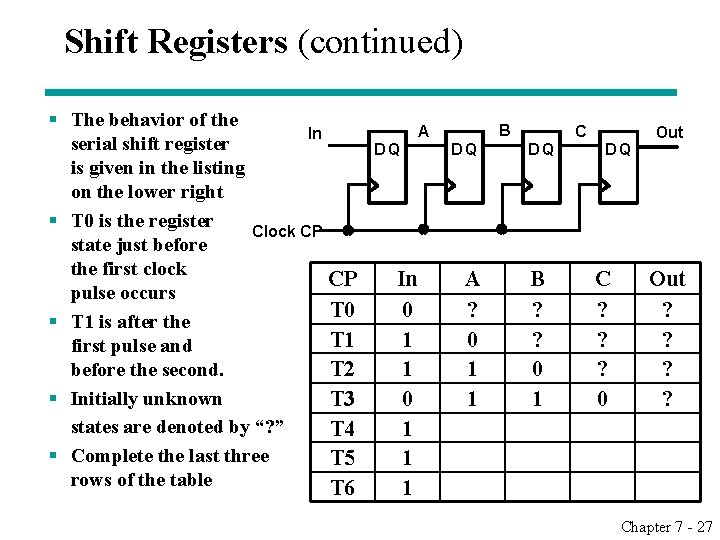
Shift Registers (continued) § The behavior of the In serial shift register is given in the listing on the lower right § T 0 is the register Clock CP state just before the first clock CP pulse occurs T 0 § T 1 is after the T 1 first pulse and before the second. T 2 § Initially unknown T 3 states are denoted by “? ” T 4 § Complete the last three T 5 rows of the table T 6 B A DQ In 0 1 1 1 DQ A ? 0 1 1 C DQ B ? ? 0 1 DQ C ? ? ? 0 Out ? ? Chapter 7 - 27

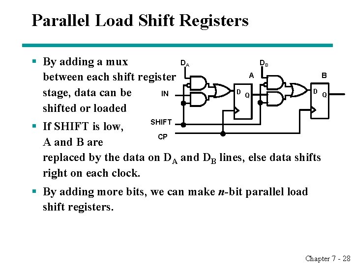
Parallel Load Shift Registers § By adding a mux between each shift register IN stage, data can be shifted or loaded DA DB A D B D Q Q SHIFT § If SHIFT is low, CP A and B are replaced by the data on DA and DB lines, else data shifts right on each clock. § By adding more bits, we can make n-bit parallel load shift registers. Chapter 7 - 28

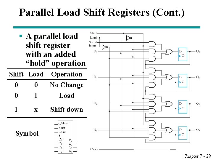
Parallel Load Shift Registers (Cont. ) § A parallel load shift register with an added “hold” operation Shift Load Operation 0 0 No Change 0 1 Load 1 x Shift down Symbol Chapter 7 - 29

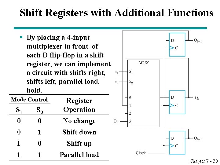
Shift Registers with Additional Functions § By placing a 4 -input multiplexer in front of each D flip-flop in a shift register, we can implement a circuit with shifts right, shifts left, parallel load, hold. Mode Control Register Operation S 1 S 0 0 0 No change 0 1 Shift down 1 0 Shift up 1 1 Parallel load Chapter 7 - 30

7. 6. 3 Counters § Counters are sequential circuits which "count" through a specific state sequence. They can count up, count down, or count through other fixed sequences. Two distinct types are in common usage: § Ripple Counters • Clock is connected to the flip-flop clock input on the LSB bit flip-flop • For all other bits, a flip-flop output is connected to the clock input, thus circuit is not truly synchronous • Output change is delayed more for each bit toward the MSB. • Resurgent because of low power consumption § Synchronous Counters • Clock is directly connected to the flip-flop clock inputs • Logic is used to implement the desired state sequencing Chapter 7 - 31

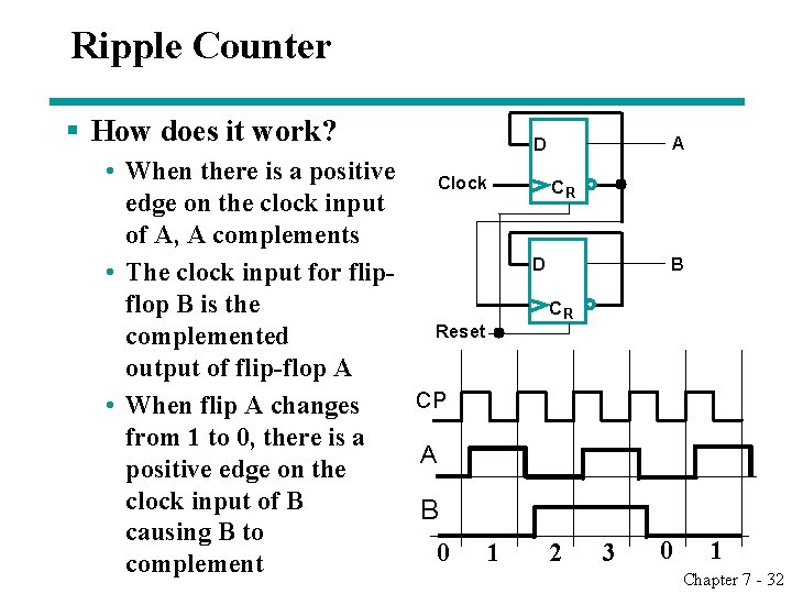
Ripple Counter § How does it work? • When there is a positive Clock edge on the clock input of A, A complements • The clock input for flipflop B is the Reset complemented output of flip-flop A CP • When flip A changes from 1 to 0, there is a A positive edge on the clock input of B B causing B to 0 1 complement A D CR D B CR 2 3 0 1 Chapter 7 - 32

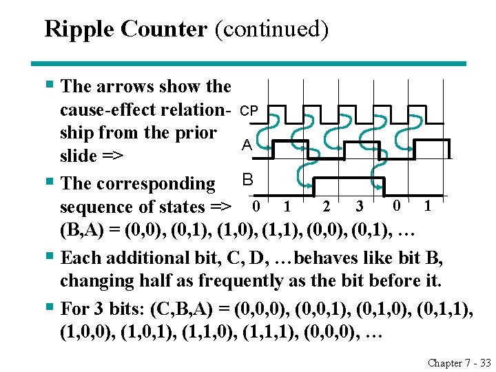
Ripple Counter (continued) § The arrows show the cause-effect relation- CP ship from the prior A slide => § The corresponding B 0 1 2 3 sequence of states => 0 1 (B, A) = (0, 0), (0, 1), (1, 0), (1, 1), (0, 0), (0, 1), … § Each additional bit, C, D, …behaves like bit B, changing half as frequently as the bit before it. § For 3 bits: (C, B, A) = (0, 0, 0), (0, 0, 1), (0, 1, 0), (0, 1, 1), (1, 0, 0), (1, 0, 1), (1, 1, 0), (1, 1, 1), (0, 0, 0), … Chapter 7 - 33

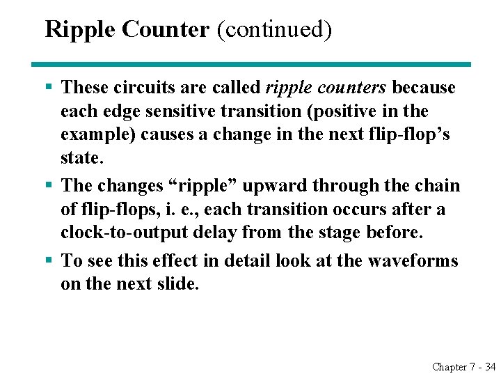
Ripple Counter (continued) § These circuits are called ripple counters because each edge sensitive transition (positive in the example) causes a change in the next flip-flop’s state. § The changes “ripple” upward through the chain of flip-flops, i. e. , each transition occurs after a clock-to-output delay from the stage before. § To see this effect in detail look at the waveforms on the next slide. Chapter 7 - 34

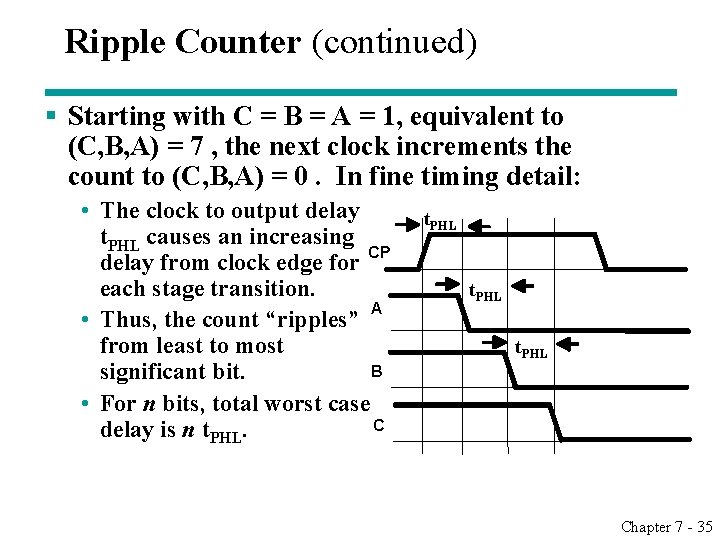
Ripple Counter (continued) § Starting with C = B = A = 1, equivalent to (C, B, A) = 7 , the next clock increments the count to (C, B, A) = 0. In fine timing detail: • The clock to output delay t. PHL causes an increasing delay from clock edge for CP each stage transition. A • Thus, the count “ripples” from least to most B significant bit. • For n bits, total worst case C delay is n t. PHL Chapter 7 - 35

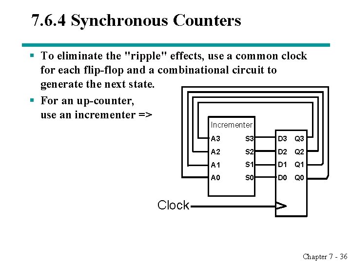
7. 6. 4 Synchronous Counters § To eliminate the "ripple" effects, use a common clock for each flip-flop and a combinational circuit to generate the next state. § For an up-counter, use an incrementer => Incrementer A 3 S 3 D 3 Q 3 A 2 S 2 D 2 Q 2 A 1 S 1 D 1 Q 1 A 0 S 0 D 0 Q 0 Clock Chapter 7 - 36

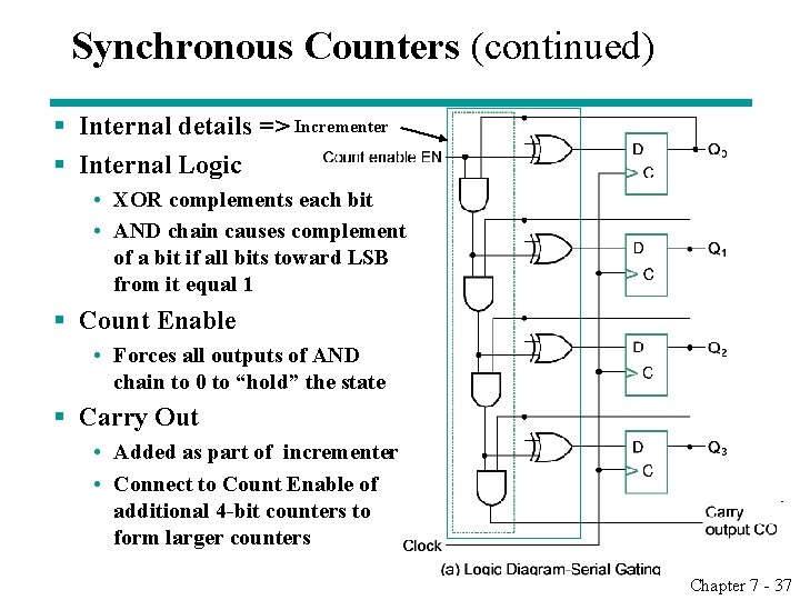
Synchronous Counters (continued) § Internal details => Incrementer § Internal Logic • XOR complements each bit • AND chain causes complement of a bit if all bits toward LSB from it equal 1 § Count Enable • Forces all outputs of AND chain to 0 to “hold” the state § Carry Out • Added as part of incrementer • Connect to Count Enable of additional 4 -bit counters to form larger counters Chapter 7 - 37

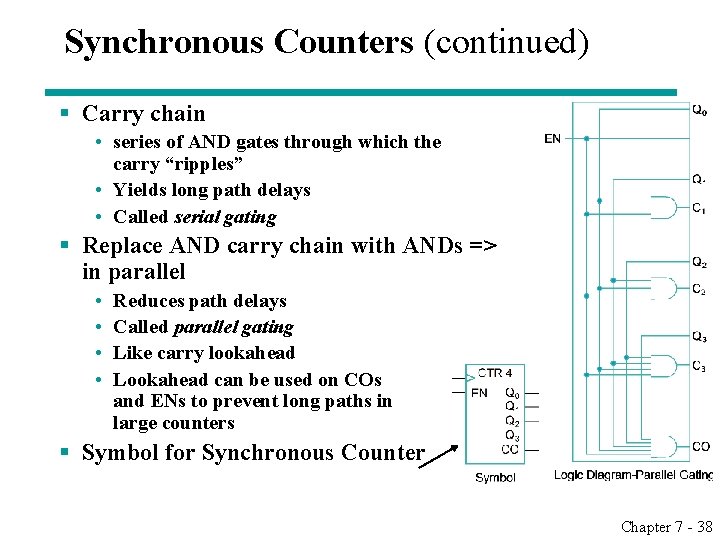
Synchronous Counters (continued) § Carry chain • series of AND gates through which the carry “ripples” • Yields long path delays • Called serial gating § Replace AND carry chain with ANDs => in parallel • • Reduces path delays Called parallel gating Like carry lookahead Lookahead can be used on COs and ENs to prevent long paths in large counters § Symbol for Synchronous Counter Chapter 7 - 38

7. 6. 5 Other Counters § See text for: • Down Counter - counts downward instead of upward • Up-Down Counter - counts up or down depending on value a control input such as Up/Down • Parallel Load Counter - Has parallel load of values available depending on control input such as Load § Divide-by-n (Modulo n) Counter • Count is remainder of division by n which n may not be a power of 2 or • Count is arbitrary sequence of n states specifically designed state-by-state • Includes modulo 10 which is the BCD counter Chapter 7 - 39

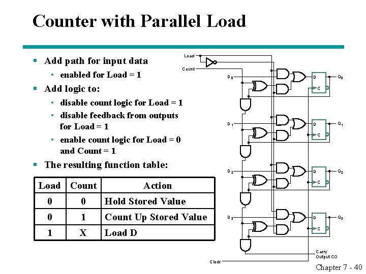
Counter with Parallel Load § Add path for input data • enabled for Load = 1 Load Count D 0 Q 0 D § Add logic to: C • disable count logic for Load = 1 • disable feedback from outputs for Load = 1 • enable count logic for Load = 0 and Count = 1 D 1 C § The resulting function table: Load Count D 2 0 Hold Stored Value 0 1 Count Up Stored Value 1 X Load D Q 2 D Action 0 Q 1 D C D 3 Q 3 D C Clock Carry Output CO Chapter 7 - 40

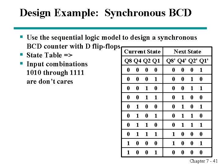
Design Example: Synchronous BCD § Use the sequential logic model to design a synchronous BCD counter with D flip-flops § State Table => § Input combinations 1010 through 1111 are don’t cares Current State Next State Q 8 Q 4 Q 2 Q 1 Q 8' Q 4' Q 2' Q 1' 0 0 0 1 0 0 1 0 0 0 1 1 0 1 0 0 0 1 0 1 1 0 0 1 1 1 1 0 0 0 1 0 0 1 0 0 Chapter 7 - 41

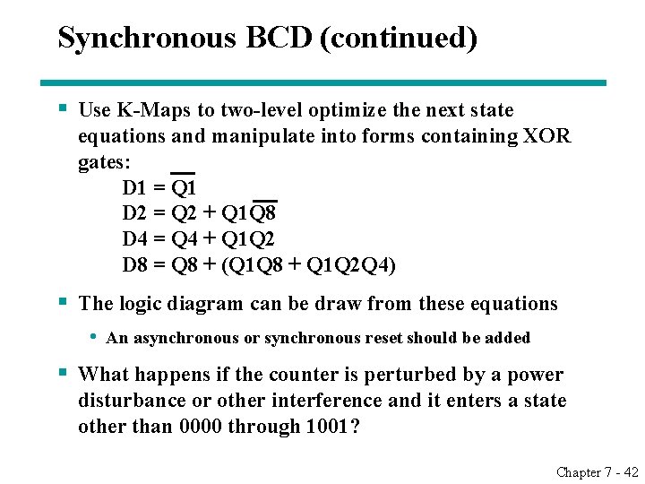
Synchronous BCD (continued) § Use K-Maps to two-level optimize the next state equations and manipulate into forms containing XOR gates: D 1 = Q 1 D 2 = Q 2 + Q 1 Q 8 D 4 = Q 4 + Q 1 Q 2 D 8 = Q 8 + (Q 1 Q 8 + Q 1 Q 2 Q 4) § The logic diagram can be draw from these equations • An asynchronous or synchronous reset should be added § What happens if the counter is perturbed by a power disturbance or other interference and it enters a state other than 0000 through 1001? Chapter 7 - 42

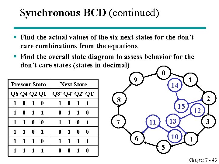
Synchronous BCD (continued) § Find the actual values of the six next states for the don’t care combinations from the equations § Find the overall state diagram to assess behavior for the don’t care states (states in decimal) 0 9 1 Present State Next State 14 Q 8 Q 4 Q 2 Q 1 Q 8' Q 4' Q 2' Q 1' 1 0 1 1 0 1 1 0 0 1 1 0 1 0 0 1 1 1 1 0 0 1 0 8 2 15 7 12 13 11 10 6 3 4 5 Chapter 7 - 43

Synchronous BCD (continued) § For the BCD counter design, if an invalid state is entered, return to a valid state occurs within two clock cycles § Is this adequate? If not: • Is a signal needed that indicates that an invalid state has been entered? What is the equation for such a signal? • Does the design need to be modified to return from an invalid state to a valid state in one clock cycle? • Does the design need to be modified to return from a invalid state to a specific state (such as 0)? § The action to be taken depends on: • the application of the circuit • design group policy Chapter 7 - 44

Counting Modulo N § The following techniques use an n-bit binary counter with asynchronous or synchronous clear and/or parallel load: • Detect a terminal count of N in a Modulo-N count sequence to asynchronously Clear the count to 0 or asynchronously Load in value 0 (These lead to counts which are present for only a very short time and can fail to work for some timing conditions!) • Detect a terminal count of N - 1 in a Modulo-N count sequence to Clear the count synchronously to 0 • Detect a terminal count of N - 1 in a Modulo-N count sequence to synchronously Load in value 0 • Detect a terminal count and use Load to preset a count of the terminal count value minus (N - 1) § Alternatively, custom design a modulo N counter as Chapter 7 - 45 done for BCD

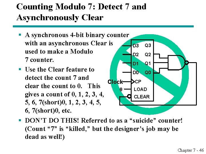
Counting Modulo 7: Detect 7 and Asynchronously Clear § A synchronous 4 -bit binary counter with an asynchronous Clear is D 3 Q 3 used to make a Modulo D 2 Q 2 7 counter. D 1 Q 1 § Use the Clear feature to D 0 Q 0 detect the count 7 and CP Clock clear the count to 0. This LOAD 0 gives a count of 0, 1, 2, 3, 4, CLEAR 5, 6, 7(short)0, 1, 2, 3, 4, 5, 6, 7(short)0, etc. § DON’T DO THIS! Referred to as a “suicide” counter! (Count “ 7” is “killed, ” but the designer’s job may be dead as well!) Chapter 7 - 46

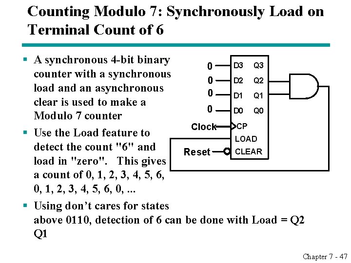
Counting Modulo 7: Synchronously Load on Terminal Count of 6 § A synchronous 4 -bit binary D 3 Q 3 0 counter with a synchronous D 2 Q 2 0 load an asynchronous 0 D 1 Q 1 clear is used to make a 0 D 0 Q 0 Modulo 7 counter CP Clock § Use the Load feature to LOAD detect the count "6" and CLEAR Reset load in "zero". This gives a count of 0, 1, 2, 3, 4, 5, 6, 0, . . . § Using don’t cares for states above 0110, detection of 6 can be done with Load = Q 2 Q 1 Chapter 7 - 47

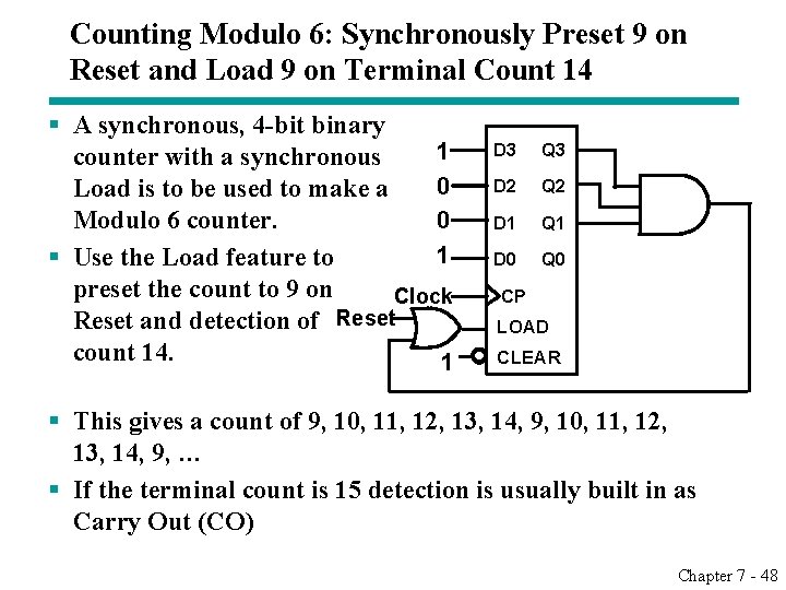
Counting Modulo 6: Synchronously Preset 9 on Reset and Load 9 on Terminal Count 14 § A synchronous, 4 -bit binary 1 counter with a synchronous 0 Load is to be used to make a Modulo 6 counter. 0 1 § Use the Load feature to preset the count to 9 on Clock Reset and detection of Reset count 14. 1 D 3 Q 3 D 2 Q 2 D 1 Q 1 D 0 Q 0 CP LOAD CLEAR § This gives a count of 9, 10, 11, 12, 13, 14, 9, 10, 11, 12, 13, 14, 9, … § If the terminal count is 15 detection is usually built in as Carry Out (CO) Chapter 7 - 48

Assignment § 7 -6、7 -12、7 -15、7 -16、7 -17、7 -20、7 -24、730 Chapter 7 - 49