Logic and Computer Design Fundamentals Chapter 7 Registers


- Slides: 27

Logic and Computer Design Fundamentals Chapter 7 – Registers and Register Transfers Part 1 – Registers, Microoperations and Implementations Charles Kime & Thomas Kaminski © 2004 Pearson Education, Inc. Terms of Use (Hyperlinks are active in View Show mode)

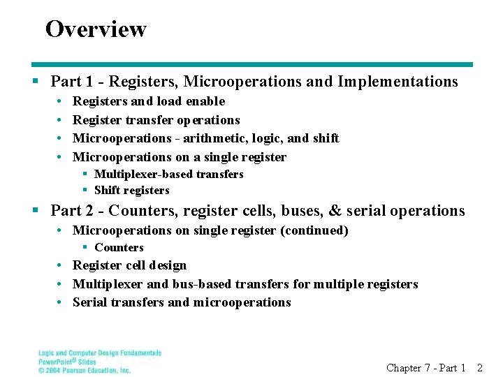
Overview § Part 1 - Registers, Microoperations and Implementations • • Registers and load enable Register transfer operations Microoperations - arithmetic, logic, and shift Microoperations on a single register § Multiplexer-based transfers § Shift registers § Part 2 - Counters, register cells, buses, & serial operations • Microoperations on single register (continued) § Counters • Register cell design • Multiplexer and bus-based transfers for multiple registers • Serial transfers and microoperations Chapter 7 - Part 1 2

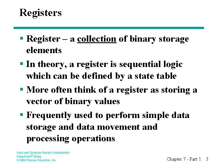
Registers § Register – a collection of binary storage elements § In theory, a register is sequential logic which can be defined by a state table § More often think of a register as storing a vector of binary values § Frequently used to perform simple data storage and data movement and processing operations Chapter 7 - Part 1 3

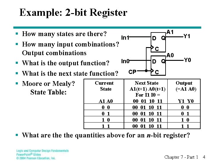
Example: 2 -bit Register A 1 § How many states are there? Y 1 In 1 D Q § How many input combinations? C Output combinations A 0 Y 0 In 0 D Q § What is the output function? C § What is the next state function? CP Current Next State Output § Moore or Mealy? State A 1 A 0 0 1 1 A 1(t+1) A 0(t+1) For I 1 I 0 = 00 01 10 11 00 01 10 11 (=A 1 A 0) Y 1 Y 0 0 1 1 0 1 1 § What are the quantities above for an n-bit register? Chapter 7 - Part 1 4

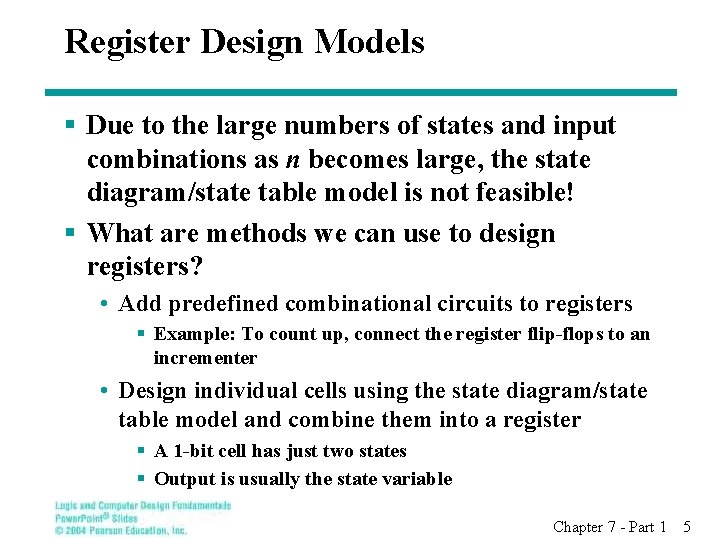
Register Design Models § Due to the large numbers of states and input combinations as n becomes large, the state diagram/state table model is not feasible! § What are methods we can use to design registers? • Add predefined combinational circuits to registers § Example: To count up, connect the register flip-flops to an incrementer • Design individual cells using the state diagram/state table model and combine them into a register § A 1 -bit cell has just two states § Output is usually the state variable Chapter 7 - Part 1 5

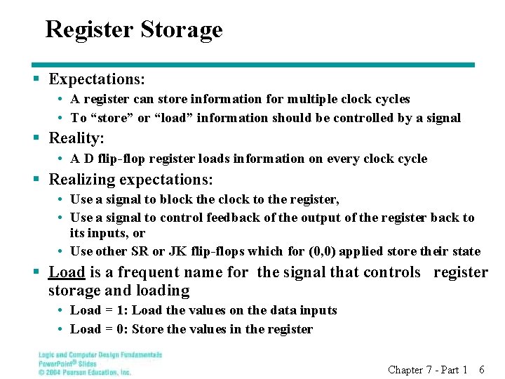
Register Storage § Expectations: • A register can store information for multiple clock cycles • To “store” or “load” information should be controlled by a signal § Reality: • A D flip-flop register loads information on every clock cycle § Realizing expectations: • Use a signal to block the clock to the register, • Use a signal to control feedback of the output of the register back to its inputs, or • Use other SR or JK flip-flops which for (0, 0) applied store their state § Load is a frequent name for the signal that controls register storage and loading • Load = 1: Load the values on the data inputs • Load = 0: Store the values in the register Chapter 7 - Part 1 6

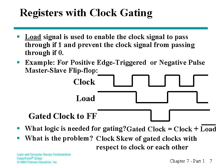
Registers with Clock Gating § Load signal is used to enable the clock signal to pass through if 1 and prevent the clock signal from passing through if 0. § Example: For Positive Edge-Triggered or Negative Pulse Master-Slave Flip-flop: Clock Load Gated Clock to FF § What logic is needed for gating? Gated Clock = Clock + Load § What is the problem? Clock Skew of gated clocks with respect to clock or each other Chapter 7 - Part 1 7

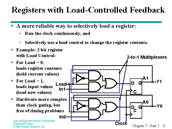
Registers with Load-Controlled Feedback § A more reliable way to selectively load a register: • Run the clock continuously, and § § • Selectively use a load control to change the register contents. Example: 2 -bit register with Load Control: 2 -to-1 Multiplexers For Load = 0, loads register contents (hold current values) A 1 For Load = 1, Y 1 D Q Load loads input values In 1 C (load new values) Hardware more complex A 0 than clock gating, but Y 0 D Q C free of timing problems In 0 Clock Chapter 7 - Part 1 8

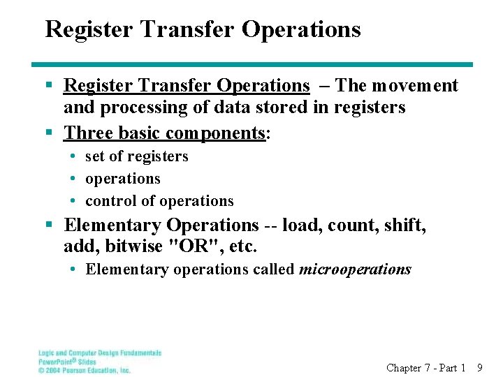
Register Transfer Operations § Register Transfer Operations – The movement and processing of data stored in registers § Three basic components: • set of registers • operations • control of operations § Elementary Operations -- load, count, shift, add, bitwise "OR", etc. • Elementary operations called microoperations Chapter 7 - Part 1 9

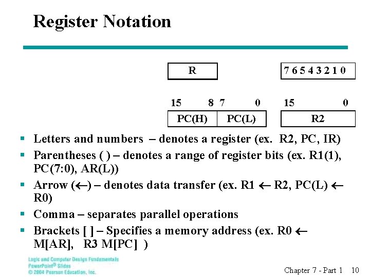
Register Notation R 7 6 5 4 3 2 1 0 15 8 7 0 15 0 PC(H) PC(L) R 2 § Letters and numbers – denotes a register (ex. R 2, PC, IR) § Parentheses ( ) – denotes a range of register bits (ex. R 1(1), PC(7: 0), AR(L)) § Arrow ( ) – denotes data transfer (ex. R 1 R 2, PC(L) R 0) § Comma – separates parallel operations § Brackets [ ] – Specifies a memory address (ex. R 0 M[AR], R 3 M[PC] ) Chapter 7 - Part 1 10

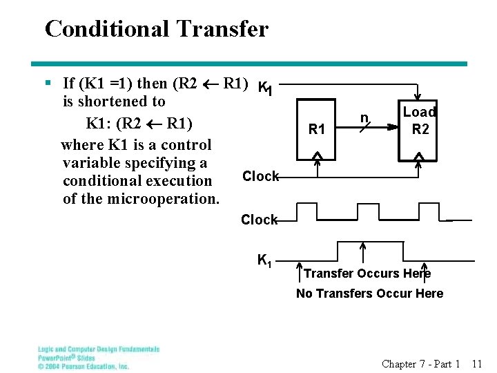
Conditional Transfer § If (K 1 =1) then (R 2 R 1) K 1 is shortened to K 1: (R 2 R 1) where K 1 is a control variable specifying a Clock conditional execution of the microoperation. R 1 n Load R 2 Clock K 1 Transfer Occurs Here No Transfers Occur Here Chapter 7 - Part 1 11

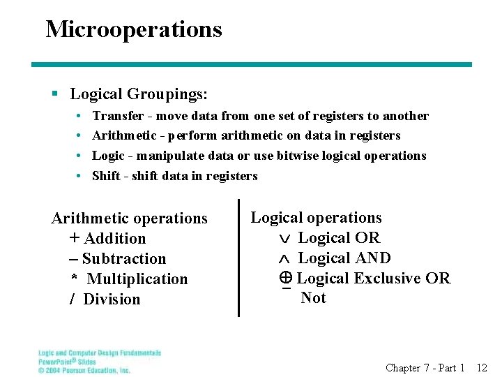
Microoperations § Logical Groupings: • • Transfer - move data from one set of registers to another Arithmetic - perform arithmetic on data in registers Logic - manipulate data or use bitwise logical operations Shift - shift data in registers Arithmetic operations + Addition – Subtraction * Multiplication / Division Logical operations Logical OR Logical AND Logical Exclusive OR Not Chapter 7 - Part 1 12

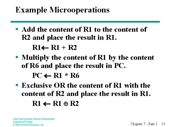
Example Microoperations § Add the content of R 1 to the content of R 2 and place the result in R 1 + R 2 § Multiply the content of R 1 by the content of R 6 and place the result in PC. PC R 1 * R 6 § Exclusive OR the content of R 1 with the content of R 2 and place the result in R 1 R 2 Chapter 7 - Part 1 13

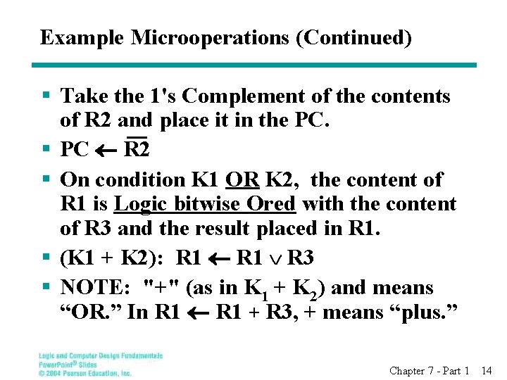
Example Microoperations (Continued) § Take the 1's Complement of the contents of R 2 and place it in the PC. § PC R 2 § On condition K 1 OR K 2, the content of R 1 is Logic bitwise Ored with the content of R 3 and the result placed in R 1. § (K 1 + K 2): R 1 R 3 § NOTE: "+" (as in K 1 + K 2) and means “OR. ” In R 1 + R 3, + means “plus. ” Chapter 7 - Part 1 14

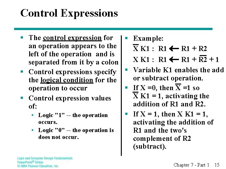
Control Expressions § The control expression for § Example: an operation appears to the X K 1 : R 1 + R 2 left of the operation and is X K 1 : R 1 + R 2 + 1 separated from it by a colon § Control expressions specify § Variable K 1 enables the add or subtract operation. the logical condition for the § If X =0, then X =1 so operation to occur X K 1 = 1, activating the § Control expression values addition of R 1 and R 2. of: § If X = 1, then X K 1 = 1, • Logic "1" -- the operation occurs. activating the addition of • Logic "0" -- the operation is R 1 and the two's does not occur. complement of R 2 (subtract). Chapter 7 - Part 1 15

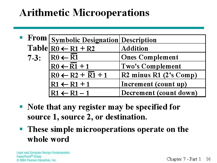
Arithmetic Microoperations § From Symbolic Designation Description Table R 0 R 1 + R 2 Addition Ones Complement 7 -3: R 0 R 1 + 1 R 0 R 2 + R 1 + 1 R 1 – 1 Two's Complement R 2 minus R 1 (2's Comp) Increment (count up) Decrement (count down) § Note that any register may be specified for source 1, source 2, or destination. § These simple microoperations operate on the whole word Chapter 7 - Part 1 16

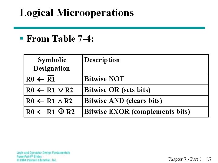
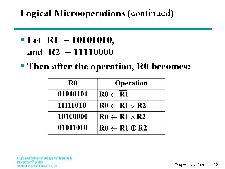
Logical Microoperations § From Table 7 -4: Symbolic Designation R 0 R 1 R 2 Description Bitwise NOT Bitwise OR (sets bits) Bitwise AND (clears bits) Bitwise EXOR (complements bits) Chapter 7 - Part 1 17

Logical Microoperations (continued) § Let R 1 = 1010, and R 2 = 11110000 § Then after the operation, R 0 becomes: Chapter 7 - Part 1 18

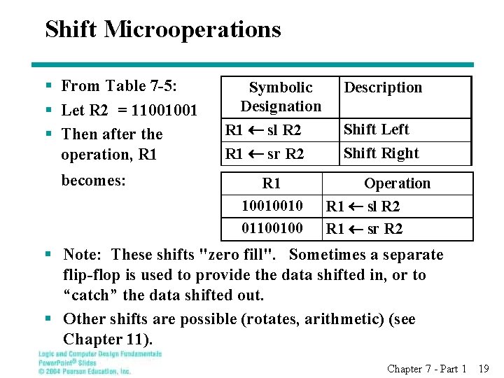
Shift Microoperations § From Table 7 -5: § Let R 2 = 11001001 § Then after the operation, R 1 becomes: Symbolic Designation R 1 sl R 2 R 1 sr R 2 Description R 1 10010010 01100100 Operation R 1 sl R 2 R 1 sr R 2 Shift Left Shift Right § Note: These shifts "zero fill". Sometimes a separate flip-flop is used to provide the data shifted in, or to “catch” the data shifted out. § Other shifts are possible (rotates, arithmetic) (see Chapter 11). Chapter 7 - Part 1 19

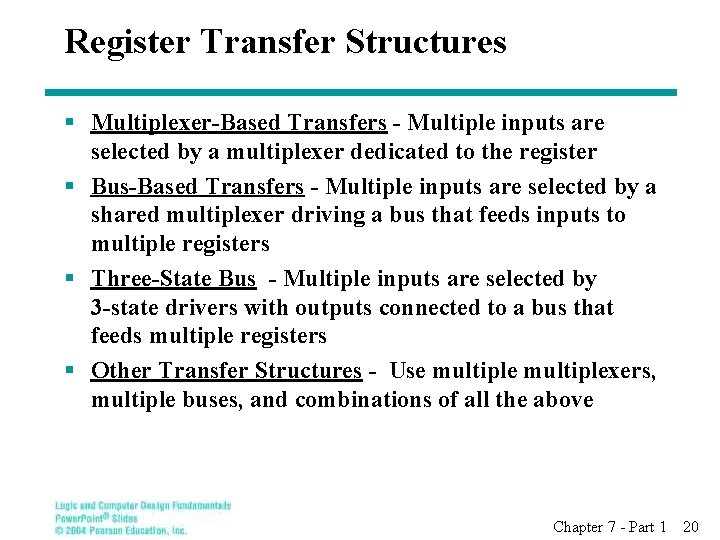
Register Transfer Structures § Multiplexer-Based Transfers - Multiple inputs are selected by a multiplexer dedicated to the register § Bus-Based Transfers - Multiple inputs are selected by a shared multiplexer driving a bus that feeds inputs to multiple registers § Three-State Bus - Multiple inputs are selected by 3 -state drivers with outputs connected to a bus that feeds multiple registers § Other Transfer Structures - Use multiplexers, multiple buses, and combinations of all the above Chapter 7 - Part 1 20

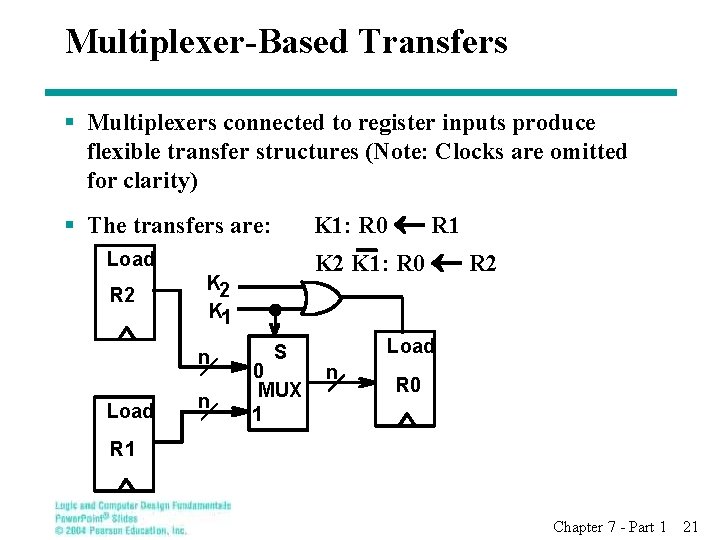
Multiplexer-Based Transfers § Multiplexers connected to register inputs produce flexible transfer structures (Note: Clocks are omitted for clarity) § The transfers are: K 1: R 0 R 1 Load K 2 K 1: R 0 R 2 K 2 K 1 n Load n S 0 MUX 1 Load n R 0 R 1 Chapter 7 - Part 1 21

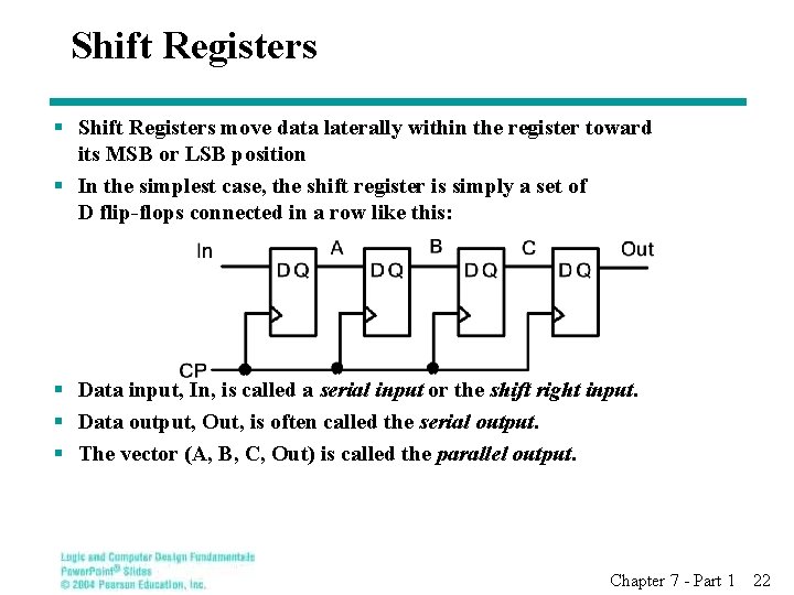
Shift Registers § Shift Registers move data laterally within the register toward its MSB or LSB position § In the simplest case, the shift register is simply a set of D flip-flops connected in a row like this: § Data input, In, is called a serial input or the shift right input. § Data output, Out, is often called the serial output. § The vector (A, B, C, Out) is called the parallel output. Chapter 7 - Part 1 22

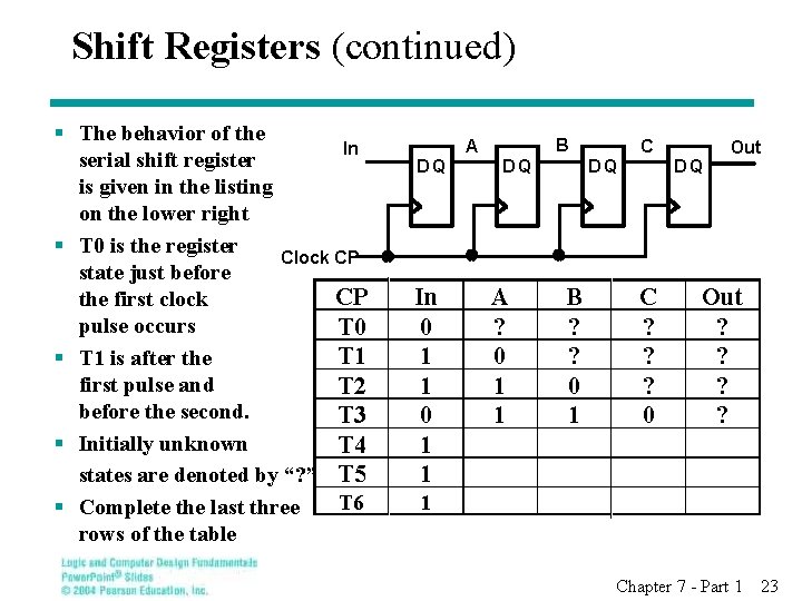
Shift Registers (continued) § The behavior of the In serial shift register is given in the listing on the lower right § T 0 is the register Clock CP state just before CP the first clock pulse occurs T 0 T 1 § T 1 is after the first pulse and T 2 before the second. T 3 § Initially unknown T 4 states are denoted by “? ” T 5 § Complete the last three T 6 rows of the table B A DQ C DQ In 0 1 1 A ? 0 1 1 1 DQ B ? ? 0 1 DQ Out C ? ? ? 0 Out ? ? Chapter 7 - Part 1 23

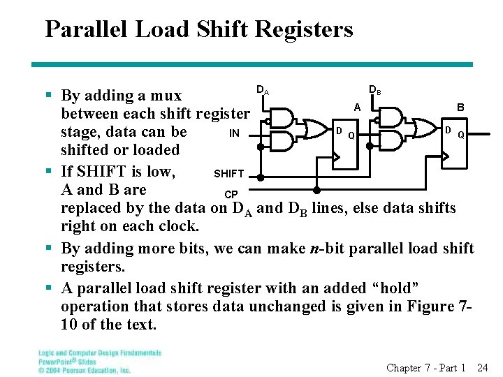
Parallel Load Shift Registers DA DB § By adding a mux A B between each shift register D D stage, data can be IN Q Q shifted or loaded § If SHIFT is low, SHIFT A and B are CP replaced by the data on DA and DB lines, else data shifts right on each clock. § By adding more bits, we can make n-bit parallel load shift registers. § A parallel load shift register with an added “hold” operation that stores data unchanged is given in Figure 710 of the text. Chapter 7 - Part 1 24

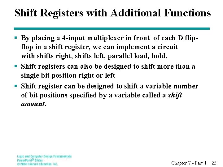
Shift Registers with Additional Functions § By placing a 4 -input multiplexer in front of each D flipflop in a shift register, we can implement a circuit with shifts right, shifts left, parallel load, hold. § Shift registers can also be designed to shift more than a single bit position right or left § Shift register can be designed to shift a variable number of bit positions specified by a variable called a shift amount. Chapter 7 - Part 1 25

Terms of Use § © 2004 by Pearson Education, Inc. All rights reserved. § The following terms of use apply in addition to the standard Pearson Education Legal Notice. § Permission is given to incorporate these materials into classroom presentations and handouts only to instructors adopting Logic and Computer Design Fundamentals as the course text. § Permission is granted to the instructors adopting the book to post these materials on a protected website or protected ftp site in original or modified form. All other website or ftp postings, including those offering the materials for a fee, are prohibited. § You may not remove or in any way alter this Terms of Use notice or any trademark, copyright, or other proprietary notice, including the copyright watermark on each slide. § Return to Title Page Chapter 7 - Part 1 26

������� ������� �� ��� ������ ������� Kingdom of Saudi Arabia Ministry of Education Umm Al. Qura University Adam University College Computer Science Department This Summary is an Online Content from this Book: Morris Mano, DIGITAL DESIGN, 4 th Edition, Prentice Hall, 2007 It is edited for Logic Analysis and Design Course 6803213 -3 by: T. Mariah Sami Khayat Teacher Assistant @ Adam University College For Contacting: mskhayat@uqu. edu. sa Chapter 1 27