Logic and Computer Design Fundamentals Chapter 5 Sequential
- Slides: 43

Logic and Computer Design Fundamentals Chapter 5 – Sequential Circuits Part 1 – Storage Elements and Sequential Circuit Analysis Charles Kime & Thomas Kaminski © 2008 Pearson Education, Inc. (Hyperlinks are active in View Show mode)

Overview § Part 1 - Storage Elements and Analysis • Introduction to sequential circuits • Types of sequential circuits • Storage elements § Latches § Flip-flops • Sequential circuit analysis § § State tables State diagrams Equivalent states Moore and Mealy Models § Part 2 - Sequential Circuit Design Chapter 5 - Part 1 2

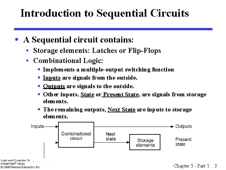
Introduction to Sequential Circuits § A Sequential circuit contains: • Storage elements: Latches or Flip-Flops • Combinational Logic: § § Implements a multiple-output switching function Inputs are signals from the outside. Outputs are signals to the outside. Other inputs, State or Present State, are signals from storage elements. § The remaining outputs, Next State are inputs to storage elements. Chapter 5 - Part 1 3

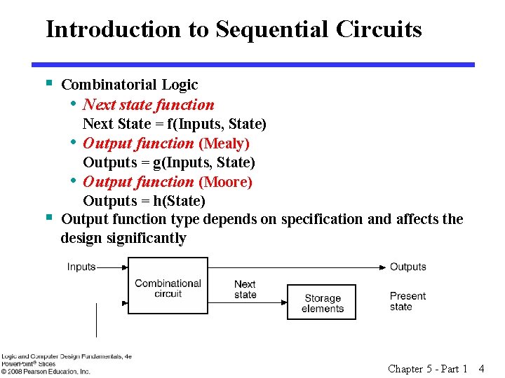
Introduction to Sequential Circuits § Combinatorial Logic • Next state function Next State = f(Inputs, State) • Output function (Mealy) Outputs = g(Inputs, State) • Output function (Moore) Outputs = h(State) § Output function type depends on specification and affects the designificantly Chapter 5 - Part 1 4

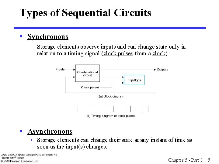
Types of Sequential Circuits § Synchronous Storage elements observe inputs and can change state only in relation to a timing signal (clock pulses from a clock) § Asynchronous • Storage elements can change their state at any instant of time as soon as the input(s) changes. Chapter 5 - Part 1 5

Comparison of Sequential Circuits § Synchronous • Easier to analyze • Choose the clock so that changes are only allowed to occur before next clock pulse § Asynchronous • Potentially faster • Harder to analyze § Will look mostly at synchronous Chapter 5 - Part 1 6

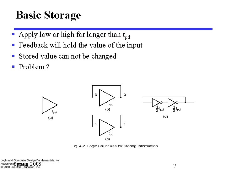
Basic Storage § § Apply low or high for longer than tpd Feedback will hold the value of the input Stored value can not be changed Problem ? Fig. 5 -2 Logic Structures for Storing Information Spring 2008 7

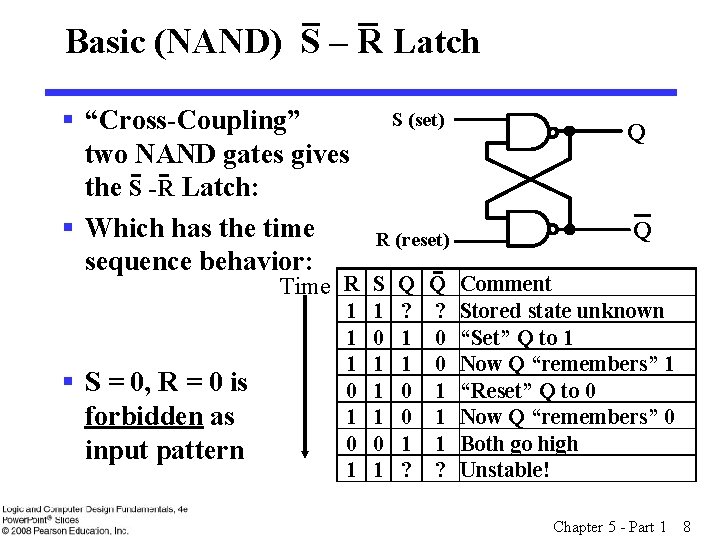
Basic (NAND) S – R Latch § “Cross-Coupling” S (set) Q two NAND gates gives the S -R Latch: § Which has the time Q R (reset) sequence behavior: Time R S Q Q Comment § S = 0, R = 0 is forbidden as input pattern 1 1 1 0 1 ? 1 1 0 0 1 ? ? 0 0 1 1 1 ? Stored state unknown “Set” Q to 1 Now Q “remembers” 1 “Reset” Q to 0 Now Q “remembers” 0 Both go high Unstable! Chapter 5 - Part 1 8

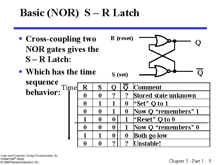
Basic (NOR) S – R Latch R (reset) § Cross-coupling two Q NOR gates gives the S – R Latch: § Which has the time Q S (set) sequence Time R S Q Q Comment behavior: 0 0 ? ? Stored state unknown 0 0 1 0 1 0 0 0 1 1 0 0 0 ? 0 0 1 1 0 ? “Set” Q to 1 Now Q “remembers” 1 “Reset” Q to 0 Now Q “remembers” 0 Both go low Unstable! Chapter 5 - Part 1 9

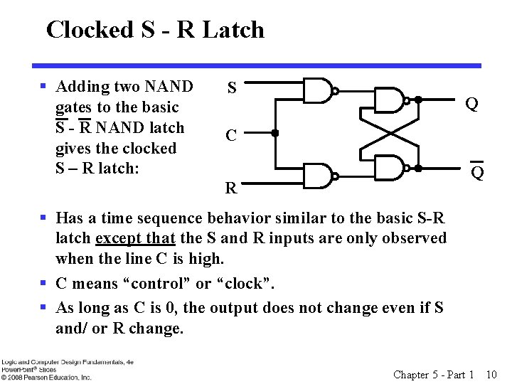
Clocked S - R Latch § Adding two NAND gates to the basic S - R NAND latch gives the clocked S – R latch: S Q C Q R § Has a time sequence behavior similar to the basic S-R latch except that the S and R inputs are only observed when the line C is high. § C means “control” or “clock”. § As long as C is 0, the output does not change even if S and/ or R change. Chapter 5 - Part 1 10

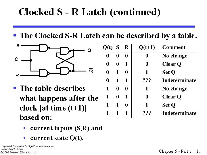
Clocked S - R Latch (continued) § The Clocked S-R Latch can be described by a table: S Q C R Q § The table describes what happens after the clock [at time (t+1)] based on: • current inputs (S, R) and • current state Q(t). Chapter 5 - Part 1 11

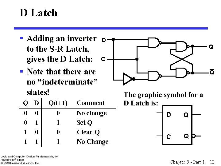
D Latch § Adding an inverter to the S-R Latch, gives the D Latch: § Note that there are no “indeterminate” states! Q 0 0 1 1 D 0 1 Q(t+1) 0 1 D Q C Comment No change Set Q Clear Q No Change Q D Q Chapter 5 - Part 1 12

Flip-Flops § The latch timing problem § Master-slave flip-flop § Edge-triggered flip-flop § Standard symbols for storage elements § Direct inputs to flip-flops Chapter 5 - Part 1 13

The Latch Timing Problem § The state of the latch is changed only when a clock pulse is available. § As long as this pulse is available, the state of the latch changes based on the latch input. § If the input to the latch changes while the pulse is available this implies a continuous change in the latch state which is used to determine next state and output. § we want the state of the latch to change once per clock pulse. Chapter 5 - Part 1 14

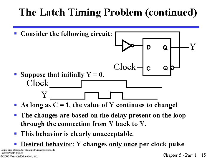
The Latch Timing Problem (continued) § Consider the following circuit: § Suppose that initially Y = 0. Clock D Q C Q Y Clock Y § As long as C = 1, the value of Y continues to change! § The changes are based on the delay present on the loop through the connection from Y back to Y. § This behavior is clearly unacceptable. § Desired behavior: Y changes only once per clock pulse Chapter 5 - Part 1 15

The Latch Timing Problem (continued) § The commonly-used solutions replace the clocked D-latch with: • a master-slave flip-flop • an edge-triggered flip-flop Chapter 5 - Part 1 16

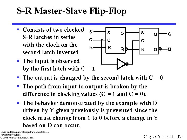
S-R Master-Slave Flip-Flop § Consists of two clocked S S S Q Q S-R latches in series C C C with the clock on the R R Q second latch inverted § The input is observed by the first latch with C = 1 § The output is changed by the second latch with C = 0 § The path from input to output is broken by the difference in clocking values (C = 1 and C = 0). § The behavior demonstrated by the example with D driven by Y given previously is prevented since the clock must change from 1 to 0 before a change in Y based on D can occur. Q Q Chapter 5 - Part 1 17

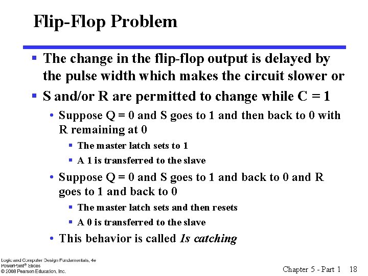
Flip-Flop Problem § The change in the flip-flop output is delayed by the pulse width which makes the circuit slower or § S and/or R are permitted to change while C = 1 • Suppose Q = 0 and S goes to 1 and then back to 0 with R remaining at 0 § The master latch sets to 1 § A 1 is transferred to the slave • Suppose Q = 0 and S goes to 1 and back to 0 and R goes to 1 and back to 0 § The master latch sets and then resets § A 0 is transferred to the slave • This behavior is called 1 s catching Chapter 5 - Part 1 18

Flip-Flop Solution § Use edge-triggering instead of master-slave § An edge-triggered flip-flop ignores the pulse while it is at a constant level and triggers only during a transition of the clock signal § Edge-triggered flip-flops can be built directly at the electronic circuit level, or § A master-slave D flip-flop which also exhibits edge-triggered behavior can be used. Chapter 5 - Part 1 19

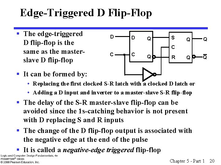
Edge-Triggered D Flip-Flop § The edge-triggered D flip-flop is the same as the masterslave D flip-flop D D Q S Q Q C C C Q R § It can be formed by: • Replacing the first clocked S-R latch with a clocked D latch or • Adding a D input and inverter to a master-slave S-R flip-flop § The delay of the S-R master-slave flip-flop can be avoided since the 1 s-catching behavior is not present with D replacing S and R inputs § The change of the D flip-flop output is associated with the negative edge at the end of the pulse § It is called a negative-edge triggered flip-flop Chapter 5 - Part 1 20

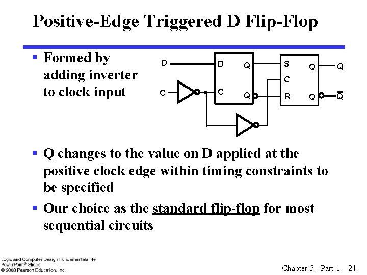
Positive-Edge Triggered D Flip-Flop § Formed by adding inverter to clock input D D Q S Q Q C C C Q R § Q changes to the value on D applied at the positive clock edge within timing constraints to be specified § Our choice as the standard flip-flop for most sequential circuits Chapter 5 - Part 1 21

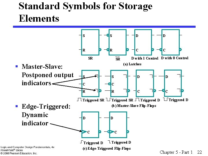
Standard Symbols for Storage Elements S S D D R R C C SR § Master-Slave: Postponed output indicators § Edge-Triggered: Dynamic indicator D with 1 Control D with 0 Control SR (a) Latches S S C C R R Triggered SR Triggered D Triggered SR (b) Master-Slave Flip-Flops D D C C Triggered D (c) Edge-Triggered Flip-Flops Chapter 5 - Part 1 22

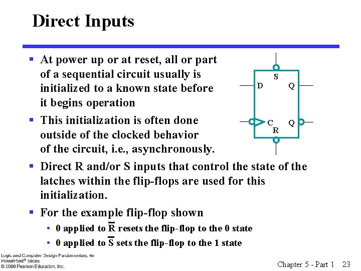
Direct Inputs § At power up or at reset, all or part of a sequential circuit usually is S D Q initialized to a known state before it begins operation § This initialization is often done C Q R outside of the clocked behavior of the circuit, i. e. , asynchronously. § Direct R and/or S inputs that control the state of the latches within the flip-flops are used for this initialization. § For the example flip-flop shown • 0 applied to R resets the flip-flop to the 0 state • 0 applied to S sets the flip-flop to the 1 state Chapter 5 - Part 1 23

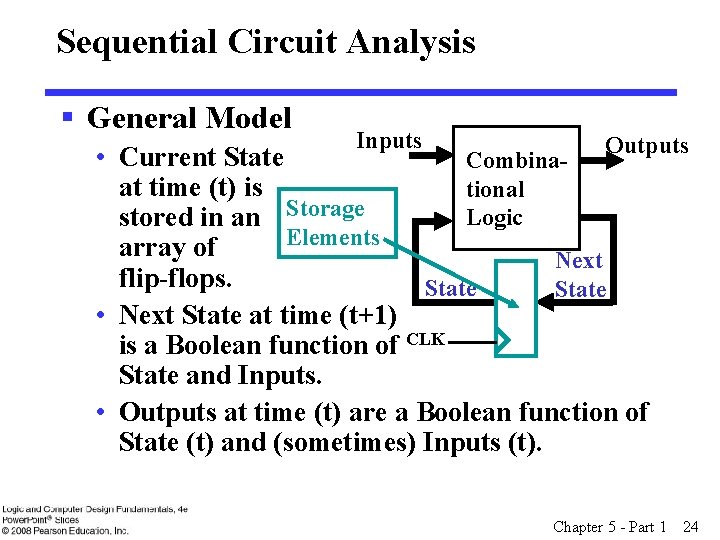
Sequential Circuit Analysis § General Model Inputs Outputs • Current State Combinaat time (t) is tional Storage Logic stored in an Elements array of Next flip-flops. State • Next State at time (t+1) CLK is a Boolean function of State and Inputs. • Outputs at time (t) are a Boolean function of State (t) and (sometimes) Inputs (t). Chapter 5 - Part 1 24

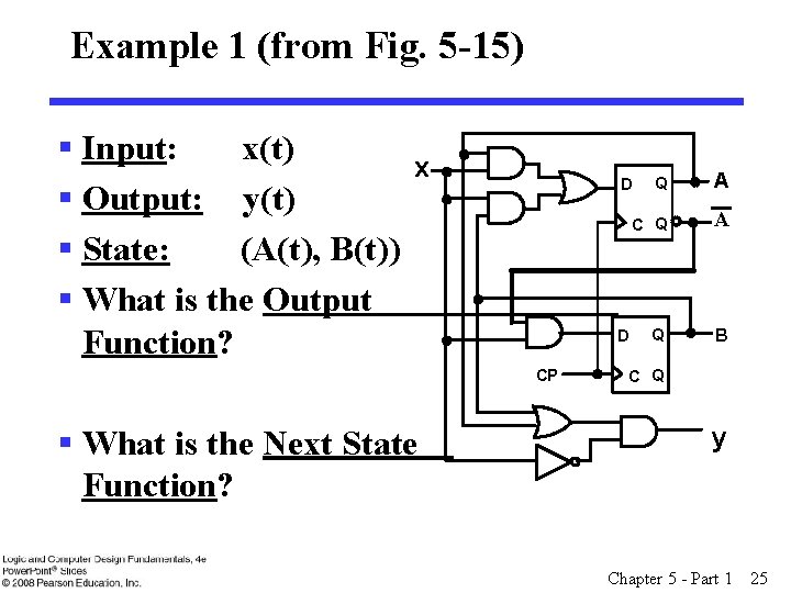
Example 1 (from Fig. 5 -15) § Input: x(t) x D Q § Output: y(t) C Q § State: (A(t), B(t)) § What is the Output D Q Function? CP A A B C Q § What is the Next State Function? y Chapter 5 - Part 1 25

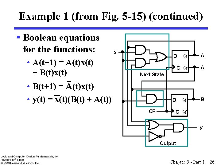
Example 1 (from Fig. 5 -15) (continued) § Boolean equations for the functions: x A D Q • A(t+1) = A(t)x(t) A C Q + B(t)x(t) Next State • B(t+1) = A(t)x(t) • y(t) = x(t)(B(t) + A(t)) CP B C Q' y Output Chapter 5 - Part 1 26

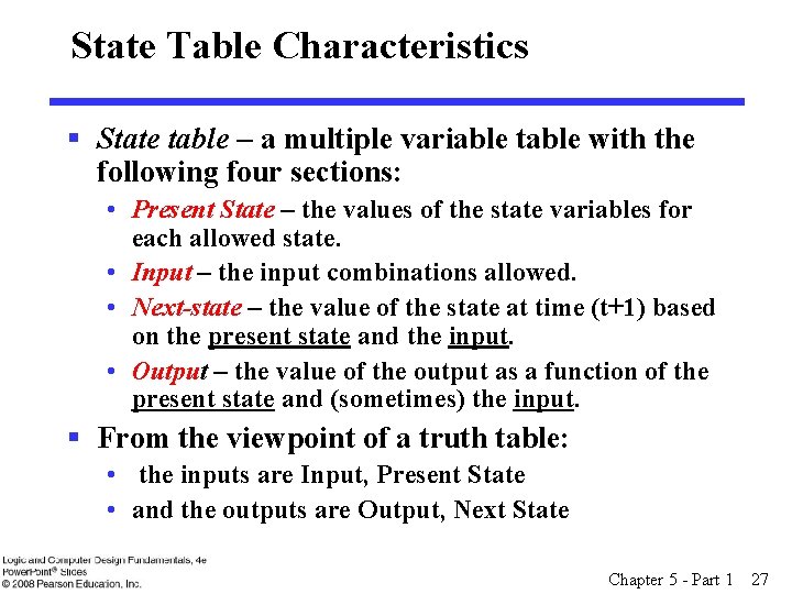
State Table Characteristics § State table – a multiple variable table with the following four sections: • Present State – the values of the state variables for each allowed state. • Input – the input combinations allowed. • Next-state – the value of the state at time (t+1) based on the present state and the input. • Output – the value of the output as a function of the present state and (sometimes) the input. § From the viewpoint of a truth table: • the inputs are Input, Present State • and the outputs are Output, Next State Chapter 5 - Part 1 27

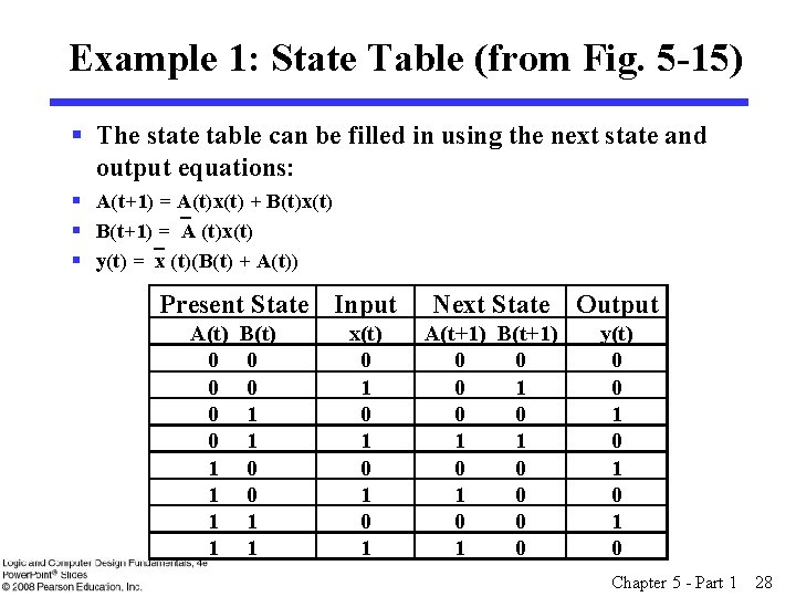
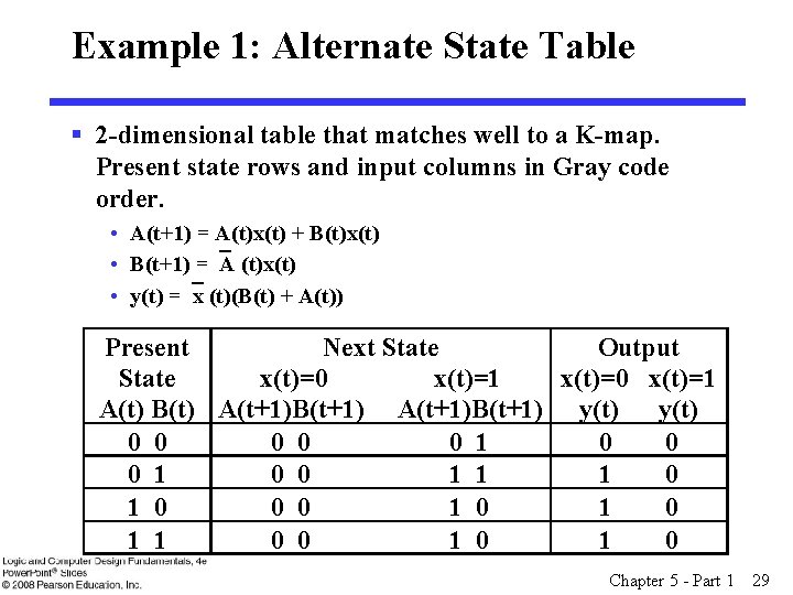
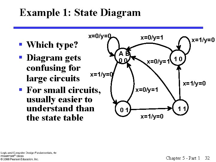
Example 1: State Table (from Fig. 5 -15) § The state table can be filled in using the next state and output equations: § A(t+1) = A(t)x(t) + B(t)x(t) § B(t+1) = A (t)x(t) § y(t) = x (t)(B(t) + A(t)) Present State Input A(t) B(t) 0 0 0 1 0 1 1 1 1 x(t) 0 1 0 1 Next State Output A(t+1) B(t+1) 0 0 0 1 0 0 1 0 y(t) 0 0 1 0 1 0 Chapter 5 - Part 1 28

Example 1: Alternate State Table § 2 -dimensional table that matches well to a K-map. Present state rows and input columns in Gray code order. • A(t+1) = A(t)x(t) + B(t)x(t) • B(t+1) = A (t)x(t) • y(t) = x (t)(B(t) + A(t)) Present Next State Output State x(t)=0 x(t)=1 x(t)=0 x(t)=1 A(t) B(t) A(t+1)B(t+1) y(t) 0 0 0 1 0 0 0 1 0 0 1 1 1 0 1 0 0 0 1 0 1 1 0 0 1 0 1 0 Chapter 5 - Part 1 29

State Diagrams § The sequential circuit function can be represented in graphical form as a state diagram with the following components: • A circle with the state name in it for each state • A directed arc from the Present State to the Next State for each state transition • A label on each directed arc with the Input values which causes the state transition, and • A label: § On each circle with the output value produced, or § On each directed arc with the output value produced. Chapter 5 - Part 1 30

State Diagrams § Label form: • On circle with output included: § state/output § Moore type output depends only on state • On directed arc with the output included: § input/output § Mealy type output depends on state and input Chapter 5 - Part 1 31

Example 1: State Diagram x=0/y=0 § Which type? § Diagram gets confusing for x=1/y=0 large circuits § For small circuits, usually easier to understand than the state table x=0/y=1 AB 00 x=0/y=1 1 0 x=0/y=1 01 x=1/y=0 11 x=1/y=0 Chapter 5 - Part 1 32

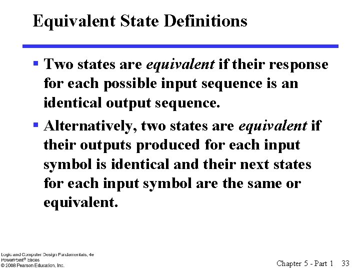
Equivalent State Definitions § Two states are equivalent if their response for each possible input sequence is an identical output sequence. § Alternatively, two states are equivalent if their outputs produced for each input symbol is identical and their next states for each input symbol are the same or equivalent. Chapter 5 - Part 1 33

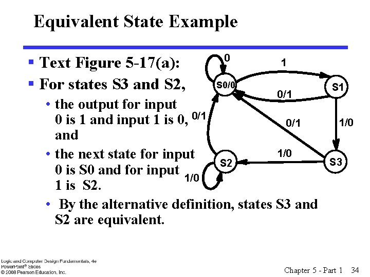
Equivalent State Example § Text Figure 5 -17(a): § For states S 3 and S 2, 0 S 0/0 1 0/1 • the output for input 0 is 1 and input 1 is 0, 0/1 and 1/0 • the next state for input S 2 0 is S 0 and for input 1/0 1 is S 2. • By the alternative definition, states S 3 and S 2 are equivalent. S 1 1/0 S 3 Chapter 5 - Part 1 34

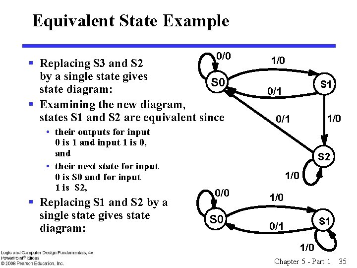
Equivalent State Example 0/0 § Replacing S 3 and S 2 by a single state gives S 0 state diagram: § Examining the new diagram, states S 1 and S 2 are equivalent since • their outputs for input 0 is 1 and input 1 is 0, and • their next state for input 0 is S 0 and for input 1 is S 2, § Replacing S 1 and S 2 by a single state gives state diagram: 1/0 S 1 0/1 1/0 0/1 S 2 1/0 0/0 S 0 1/0 S 1 0/1 1/0 Chapter 5 - Part 1 35

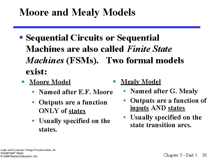
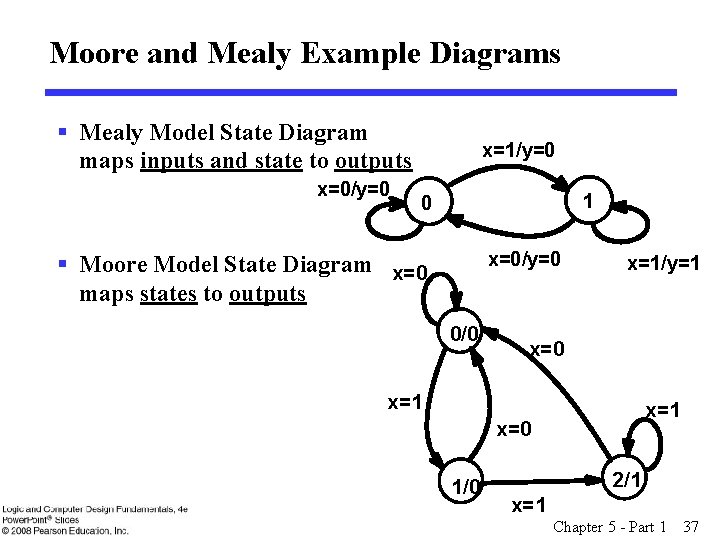
Moore and Mealy Models § Sequential Circuits or Sequential Machines are also called Finite State Machines (FSMs). Two formal models exist: § Mealy Model § Moore Model • Named after E. F. Moore • Named after G. Mealy • Outputs are a function of • Outputs are a function inputs AND states ONLY of states • Usually specified on the state transition arcs. states. Chapter 5 - Part 1 36

Moore and Mealy Example Diagrams § Mealy Model State Diagram maps inputs and state to outputs x=0/y=0 x=1/y=0 1 0 x=0/y=0 x=1/y=1 § Moore Model State Diagram x=0 maps states to outputs 0/0 x=1 x=0 1/0 2/1 x=1 Chapter 5 - Part 1 37

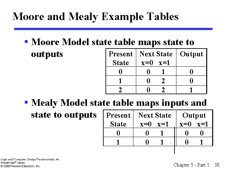
Moore and Mealy Example Tables § Moore Model state table maps state to Present Next State Output outputs State 0 1 2 x=0 x=1 0 2 0 2 0 0 1 § Mealy Model state table maps inputs and state to outputs Present Next State Output State 0 1 x=0 x=1 0 0 0 1 Chapter 5 - Part 1 38

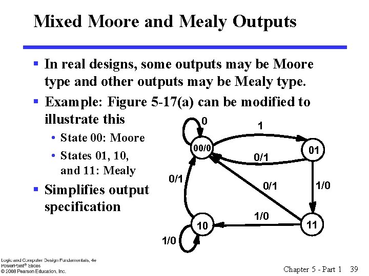
Mixed Moore and Mealy Outputs § In real designs, some outputs may be Moore type and other outputs may be Mealy type. § Example: Figure 5 -17(a) can be modified to illustrate this 0 1 • State 00: Moore • States 01, 10, and 11: Mealy § Simplifies output specification 00/0 0/1 0/1 10 1/0 01 1/0 11 1/0 Chapter 5 - Part 1 39

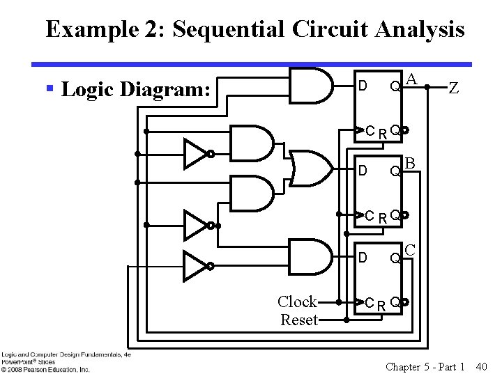
Example 2: Sequential Circuit Analysis § Logic Diagram: D Q A Z C RQ D Q B C RQ D Clock Reset Q C CR Q Chapter 5 - Part 1 40

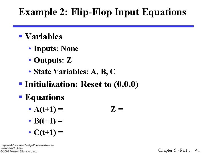
Example 2: Flip-Flop Input Equations § Variables • Inputs: None • Outputs: Z • State Variables: A, B, C § Initialization: Reset to (0, 0, 0) § Equations • A(t+1) = Z = • B(t+1) = • C(t+1) = Chapter 5 - Part 1 41

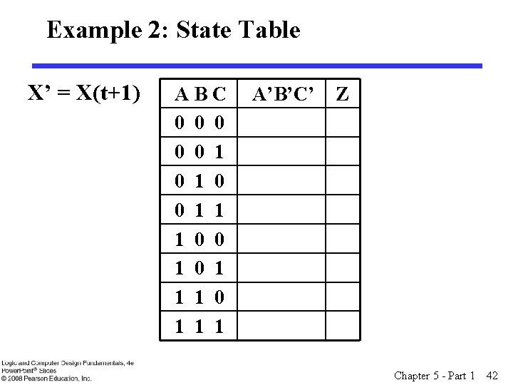
Example 2: State Table X’ = X(t+1) A B C A’B’C’ Z 0 0 0 1 0 0 1 1 1 0 0 1 0 1 1 1 0 1 1 1 Chapter 5 - Part 1 42

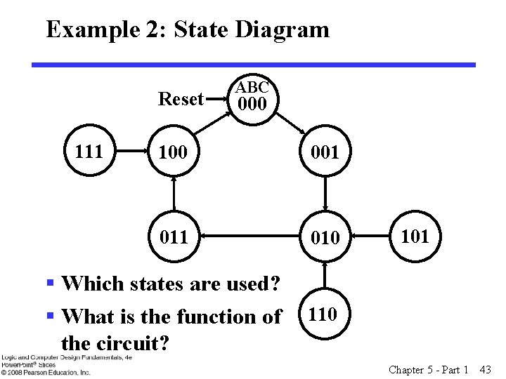
Example 2: State Diagram Reset 111 ABC 000 100 001 010 § Which states are used? § What is the function of the circuit? 101 110 Chapter 5 - Part 1 43