Logic and Computer Design Fundamentals Chapter 10 Computer


- Slides: 33

Logic and Computer Design Fundamentals Chapter 10 – Computer Design Basics Part 2 – A Simple Computer Charles Kime & Thomas Kaminski © 2004 Pearson Education, Inc. Terms of Use (Hyperlinks are active in View Show mode)

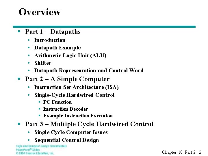
Overview § Part 1 – Datapaths • • • Introduction Datapath Example Arithmetic Logic Unit (ALU) Shifter Datapath Representation and Control Word § Part 2 – A Simple Computer • Instruction Set Architecture (ISA) • Single-Cycle Hardwired Control § PC Function § Instruction Decoder § Example Instruction Execution § Part 3 – Multiple Cycle Hardwired Control • Single Cycle Computer Issues • Sequential Control Design Chapter 10 Part 2 2

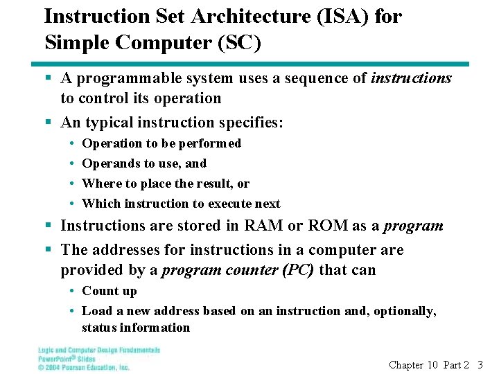
Instruction Set Architecture (ISA) for Simple Computer (SC) § A programmable system uses a sequence of instructions to control its operation § An typical instruction specifies: • • Operation to be performed Operands to use, and Where to place the result, or Which instruction to execute next § Instructions are stored in RAM or ROM as a program § The addresses for instructions in a computer are provided by a program counter (PC) that can • Count up • Load a new address based on an instruction and, optionally, status information Chapter 10 Part 2 3

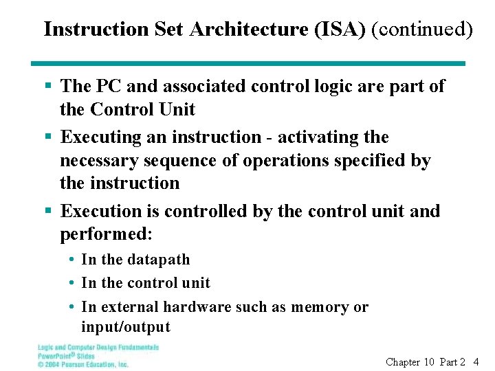
Instruction Set Architecture (ISA) (continued) § The PC and associated control logic are part of the Control Unit § Executing an instruction - activating the necessary sequence of operations specified by the instruction § Execution is controlled by the control unit and performed: • In the datapath • In the control unit • In external hardware such as memory or input/output Chapter 10 Part 2 4

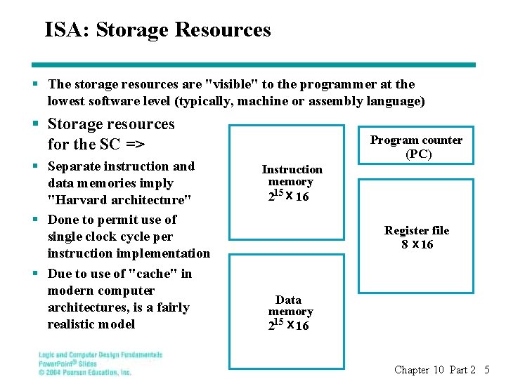
ISA: Storage Resources § The storage resources are "visible" to the programmer at the lowest software level (typically, machine or assembly language) § Storage resources for the SC => § Separate instruction and data memories imply "Harvard architecture" § Done to permit use of single clock cycle per instruction implementation § Due to use of "cache" in modern computer architectures, is a fairly realistic model Program counter (PC) Instruction memory 215 x 16 Register file 8 x 16 Data memory 215 x 16 Chapter 10 Part 2 5

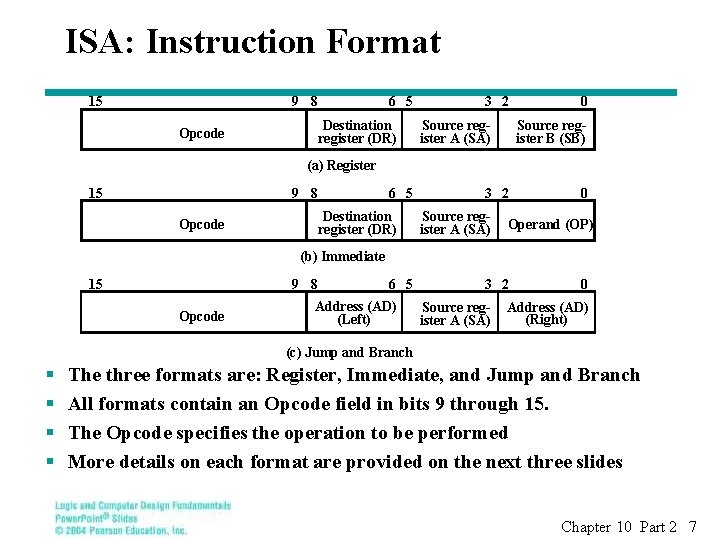
ISA: Instruction Format § A instruction consists of a bit vector § The fields of an instruction are subvectors representing specific functions and having specific binary codes defined § The format of an instruction defines the subvectors and their function § An ISA usually contains multiple formats § The SC ISA contains the three formats presented on the next slide Chapter 10 Part 2 6

ISA: Instruction Format 15 9 8 6 5 Destination register (DR) Opcode 3 2 Source register A (SA) 0 Source register B (SB) (a) Register 15 9 8 6 5 Destination register (DR) Opcode 3 2 Source register A (SA) 0 Operand (OP) (b) Immediate 15 9 8 Opcode 6 5 Address (AD) (Left) 3 2 Source register A (SA) 0 Address (AD) (Right) (c) Jump and Branch § § The three formats are: Register, Immediate, and Jump and Branch All formats contain an Opcode field in bits 9 through 15. The Opcode specifies the operation to be performed More details on each format are provided on the next three slides Chapter 10 Part 2 7

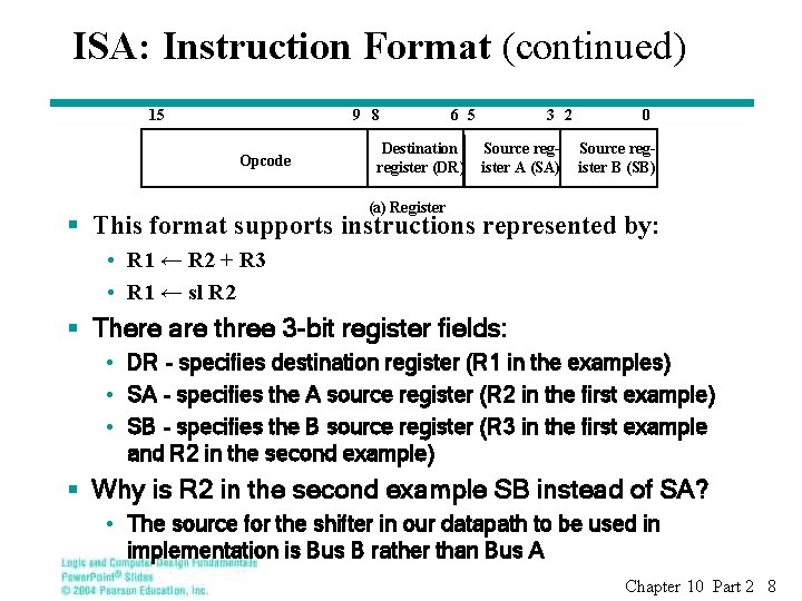
ISA: Instruction Format (continued) 15 9 8 Opcode 6 5 Destination register (DR) 3 2 Source register A (SA) 0 Source register B (SB) (a) Register § This format supports instructions represented by: • R 1 ← R 2 + R 3 • R 1 ← sl R 2 § There are three 3 -bit register fields: • DR - specifies destination register (R 1 in the examples) • SA - specifies the A source register (R 2 in the first example) • SB - specifies the B source register (R 3 in the first example and R 2 in the second example) § Why is R 2 in the second example SB instead of SA? • The source for the shifter in our datapath to be used in implementation is Bus B rather than Bus A Chapter 10 Part 2 8

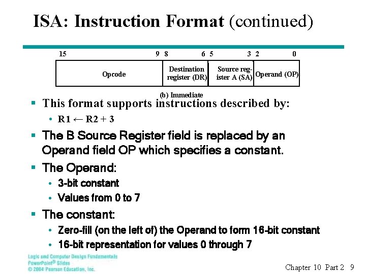
ISA: Instruction Format (continued) 15 9 8 Opcode 6 5 Destination register (DR) 3 2 0 Source register A (SA) Operand (OP) (b) Immediate § This format supports instructions described by: • R 1 ← R 2 + 3 § The B Source Register field is replaced by an Operand field OP which specifies a constant. § The Operand: • 3 -bit constant • Values from 0 to 7 § The constant: • Zero-fill (on the left of) the Operand to form 16 -bit constant • 16 -bit representation for values 0 through 7 Chapter 10 Part 2 9

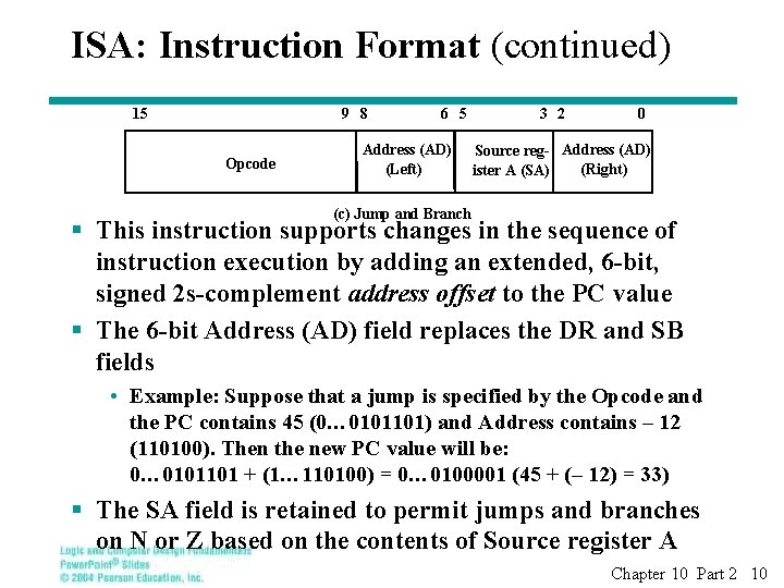
ISA: Instruction Format (continued) 15 9 8 Opcode 6 5 Address (AD) (Left) 3 2 0 Source reg- Address (AD) (Right) ister A (SA) (c) Jump and Branch § This instruction supports changes in the sequence of instruction execution by adding an extended, 6 -bit, signed 2 s-complement address offset to the PC value § The 6 -bit Address (AD) field replaces the DR and SB fields • Example: Suppose that a jump is specified by the Opcode and the PC contains 45 (0… 0101101) and Address contains – 12 (110100). Then the new PC value will be: 0… 0101101 + (1… 110100) = 0… 0100001 (45 + (– 12) = 33) § The SA field is retained to permit jumps and branches on N or Z based on the contents of Source register A Chapter 10 Part 2 10

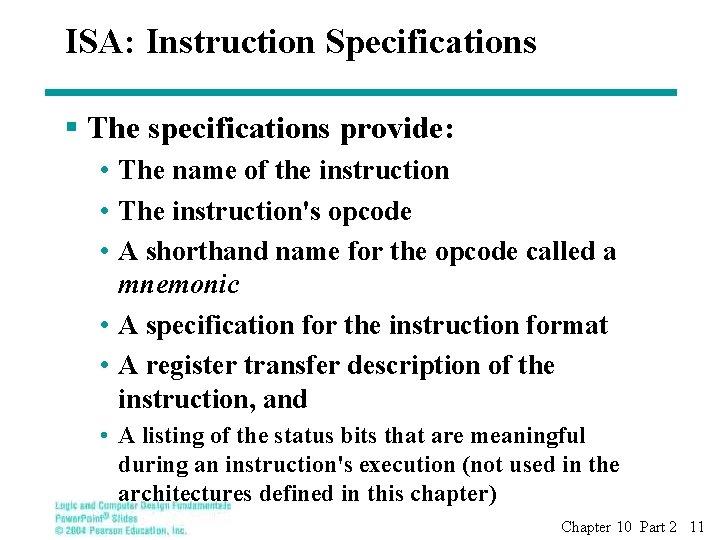
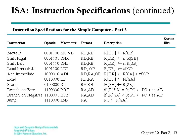
ISA: Instruction Specifications § The specifications provide: • The name of the instruction • The instruction's opcode • A shorthand name for the opcode called a mnemonic • A specification for the instruction format • A register transfer description of the instruction, and • A listing of the status bits that are meaningful during an instruction's execution (not used in the architectures defined in this chapter) Chapter 10 Part 2 11

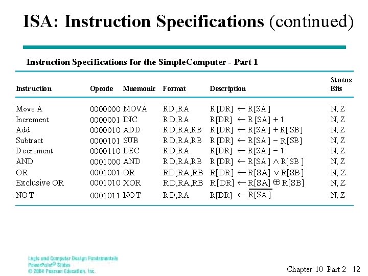
ISA: Instruction Specifications (continued) Instruction Speci fications for the Simple. Computer - Part 1 St atus Bits Instr uction Opcode Mnemonic Format Description Move A Increment Add Subtract D ecrement AND 00000001 00000101 0000110 0001001 0001010 0001011 MOVA INC ADD SUB DEC AND RD , RA R D, RA, RB R D, RA, RB R [DR] R[DR] R [DR] +1 + R[ SB] - R [SB] -1 Ù R[SB ] N, Z N, Z OR XOR RD, RA, RB R[DR] ¬ R[SA] Ú R[SB] RD, RA, RB R[DR] ¬ R[SA] Å R[SB] N, Z NO T R D, RA OR Exclusive OR NO T ¬ R[SA ] ¬ R [SA] ¬ R[SA ] R[DR] ¬ R[SA ] N, Z Chapter 10 Part 2 12

ISA: Instruction Specifications (continued) Instruction Specifications for the Simple Computer - Part 2 St atus Bits Instr uction Opcode Mnemonic Format Description Move B Shift Right Shift Left Load Immediate Add Immediate Load Store Branch on Zero Branch on Negative Jump 0001100 0001101 0001110 1001100 1000010000 0100000 1100001 1110000 MOVB SHR SHL LDI ADI LD ST BRZ BRN JMP RD , RB RD, OP RD, RA, OP RD , RA RA, RB RA, AD RA R[DR] ¬ R[SB] R[DR] ¬ sr R[SB] R[DR] ¬ sl R[SB] R[DR] ¬ zf OP R[DR] ¬ R[SA] + zf OP R[DR] ¬ M[SA] ¬ R[SB] if (R[SA] = 0) PC ¬ PC + se AD if (R[SA] < 0) PC ¬ PC + se AD PC ¬ R[SA ] Chapter 10 Part 2 13

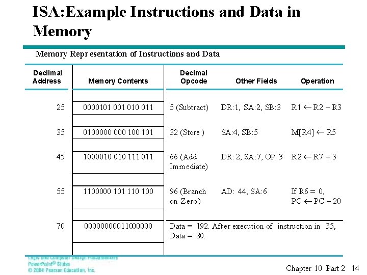
ISA: Example Instructions and Data in Memory Repr esentation of Instructions and Data Deciimal Address Memory Contents Decimal Opcode Other Fields Operation 25 0000101 010 011 5 (Subtract) DR: 1, SA: 2, SB: 3 R 1 ¬ R 2 - R 3 35 0100000 100 101 32 (Store ) SA: 4, SB: 5 M[R 4] ¬ R 5 45 1000010 111 011 66 (Add Immediate) DR: 2, SA: 7, OP : 3 R 2 ¬ R 7 + 3 55 1100000 101 110 100 96 (Branch on Zero) AD: 44, SA: 6 If R 6 = 0, PC ¬ PC - 20 70 0000011000000 Data = 192. After execution of instruction in 35, Data = 80. Chapter 10 Part 2 14

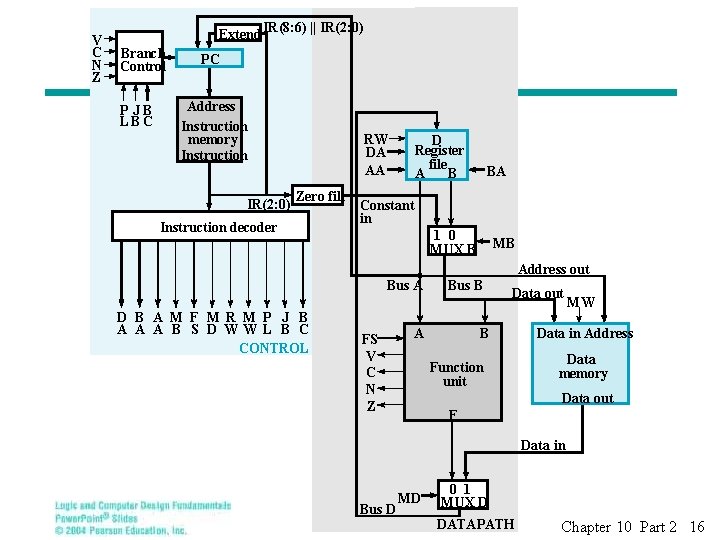
Single-Cycle Hardwired Control § Based on the ISA defined, design a computer architecture to support the ISA § The architecture is to fetch and execute each instruction in a single clock cycle § The datapath from Figure 10 -11 will be used § The control unit will be defined as a part of the design § The block diagram is shown on the next slide Chapter 10 Part 2 15

V C N Z Extend Branch Control P JB LBC IR(8: 6) || IR(2: 0) PC Address Instruction memory Instruction IR(2: 0) RW DA AA Zero fill Instruction decoder D Register file A B BA Constant in 1 0 MUX B MB Address out Bus A D B A M F M R M P J B A A A B S D WW L B C CONTROL FS V C N Z Bus B A Data out B Function unit MW Data in Address Data memory Data out F Data in Bus D MD 0 1 MUX D DATAPATH Chapter 10 Part 2 16

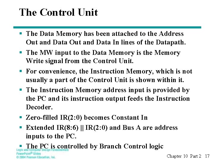
The Control Unit § The Data Memory has been attached to the Address Out and Data In lines of the Datapath. § The MW input to the Data Memory is the Memory Write signal from the Control Unit. § For convenience, the Instruction Memory, which is not usually a part of the Control Unit is shown within it. § The Instruction Memory address input is provided by the PC and its instruction output feeds the Instruction Decoder. § Zero-filled IR(2: 0) becomes Constant In § Extended IR(8: 6) || IR(2: 0) and Bus A are address inputs to the PC. § The PC is controlled by Branch Control logic Chapter 10 Part 2 17

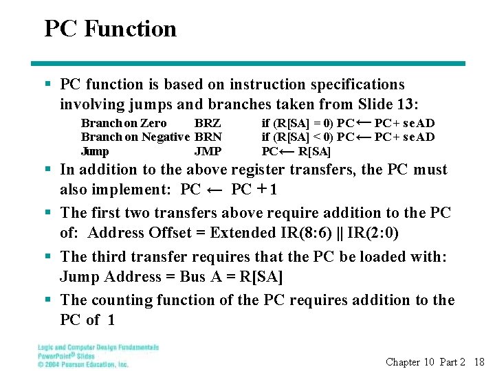
PC Function § PC function is based on instruction specifications involving jumps and branches taken from Slide 13: Branch on Zero BRZ if (R[SA] = 0) PC ← PC + se AD Branch on Negative BRN if (R[SA] < 0) PC ← PC + se AD Jump JMP PC ← R[SA] § In addition to the above register transfers, the PC must also implement: PC ← PC + 1 § The first two transfers above require addition to the PC of: Address Offset = Extended IR(8: 6) || IR(2: 0) § The third transfer requires that the PC be loaded with: Jump Address = Bus A = R[SA] § The counting function of the PC requires addition to the PC of 1 Chapter 10 Part 2 18

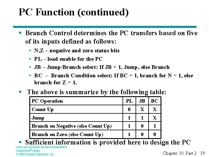
PC Function (continued) § Branch Control determines the PC transfers based on five of its inputs defined as follows: • • N, Z – negative and zero status bits PL – load enable for the PC JB – Jump/Branch select: If JB = 1, Jump, else Branch BC – Branch Condition select: If BC = 1, branch for N = 1, else branch for Z = 1. § The above is summarize by the following table: PC Operation PL JB BC Count Up 0 X X Jump 1 1 X Branch on Negative (else Count Up) 1 0 1 Branch on Zero (else Count Up) 1 0 0 § Sufficient information is provided here to design the PC Chapter 10 Part 2 19

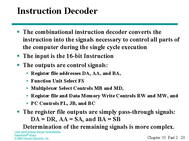
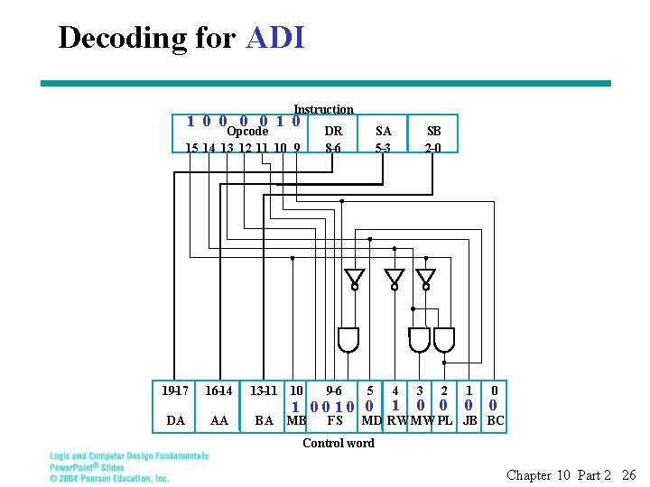
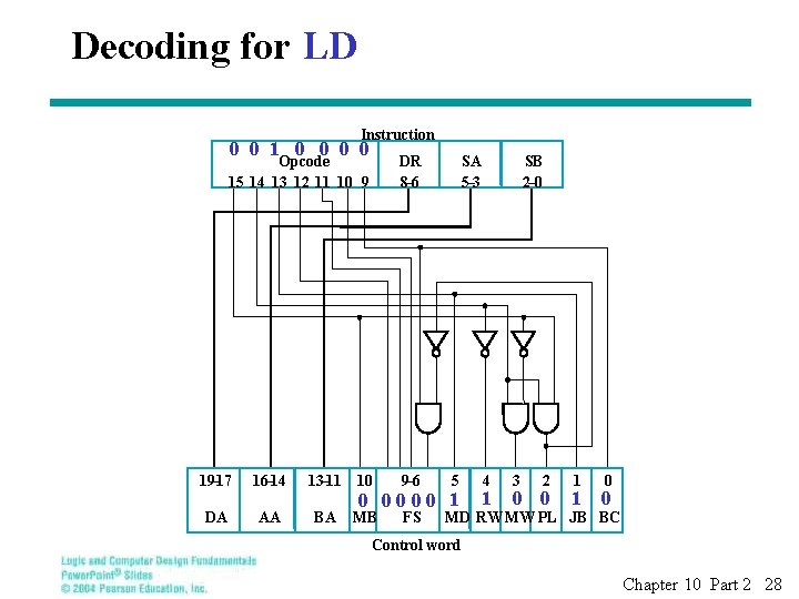
Instruction Decoder § The combinational instruction decoder converts the instruction into the signals necessary to control all parts of the computer during the single cycle execution § The input is the 16 -bit Instruction § The outputs are control signals: • • • Register file addresses DA, AA, and BA, Function Unit Select FS Multiplexer Select Controls MB and MD, Register file and Data Memory Write Controls RW and MW, and PC Controls PL, JB, and BC § The register file outputs are simply pass-through signals: DA = DR, AA = SA, and BA = SB Determination of the remaining signals is more complex. Chapter 10 Part 2 20

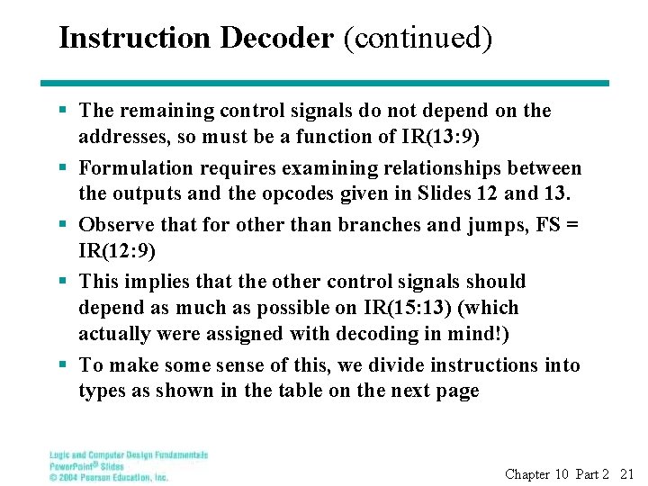
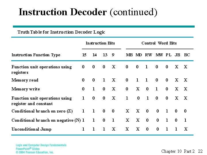
Instruction Decoder (continued) § The remaining control signals do not depend on the addresses, so must be a function of IR(13: 9) § Formulation requires examining relationships between the outputs and the opcodes given in Slides 12 and 13. § Observe that for other than branches and jumps, FS = IR(12: 9) § This implies that the other control signals should depend as much as possible on IR(15: 13) (which actually were assigned with decoding in mind!) § To make some sense of this, we divide instructions into types as shown in the table on the next page Chapter 10 Part 2 21

Instruction Decoder (continued) Truth Table for Instruction Decoder Logic Instruction Bits Control Wo rd Bits Instruction Function Type 15 14 13 9 MB MD RW MW PL JB BC Function unit operations using registers 0 0 0 X 0 0 1 0 0 X X Memory read 0 0 1 X 0 1 1 0 0 X X Memory write 0 1 0 X X Function unit operations using register and constant 1 0 0 X X Conditional branch on zero (Z) 1 1 0 0 X X 0 0 1 0 0 Conditional branch on negative (N) 1 1 0 1 X X 0 0 1 Unconditional Jump 1 1 X X X 0 0 1 1 X 1 Chapter 10 Part 2 22

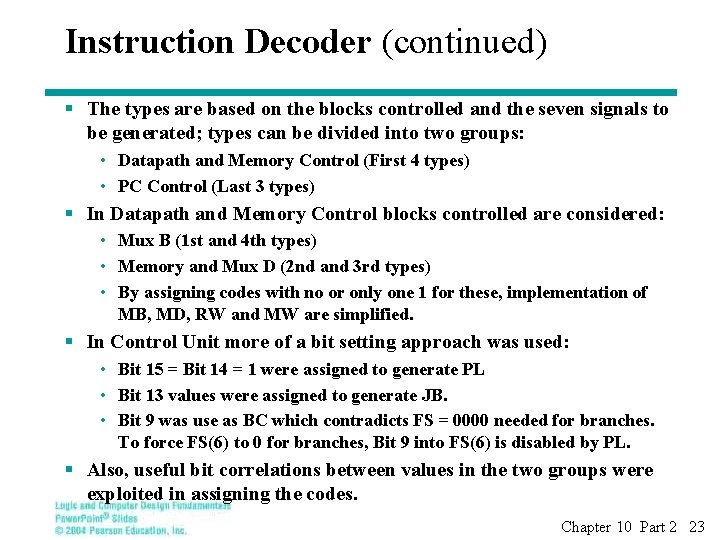
Instruction Decoder (continued) § The types are based on the blocks controlled and the seven signals to be generated; types can be divided into two groups: • Datapath and Memory Control (First 4 types) • PC Control (Last 3 types) § In Datapath and Memory Control blocks controlled are considered: • Mux B (1 st and 4 th types) • Memory and Mux D (2 nd and 3 rd types) • By assigning codes with no or only one 1 for these, implementation of MB, MD, RW and MW are simplified. § In Control Unit more of a bit setting approach was used: • Bit 15 = Bit 14 = 1 were assigned to generate PL • Bit 13 values were assigned to generate JB. • Bit 9 was use as BC which contradicts FS = 0000 needed for branches. To force FS(6) to 0 for branches, Bit 9 into FS(6) is disabled by PL. § Also, useful bit correlations between values in the two groups were exploited in assigning the codes. Chapter 10 Part 2 23

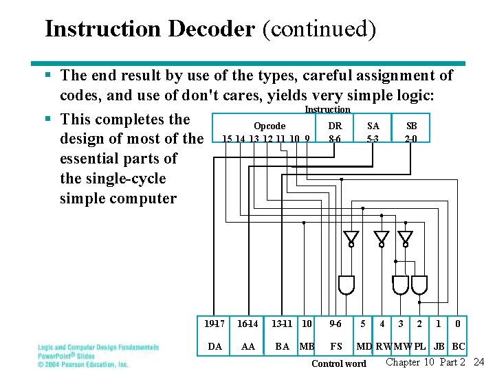
Instruction Decoder (continued) § The end result by use of the types, careful assignment of codes, and use of don't cares, yields very simple logic: Instruction § This completes the Opcode DR SA SB 5– 3 2– 0 design of most of the 15 14 13 12 11 10 9 8– 6 essential parts of the single-cycle simple computer 19– 17 16– 14 DA AA 13– 11 10 BA MB 9– 6 FS 5 4 3 2 1 0 MD RW MW PL JB BC Control word Chapter 10 Part 2 24

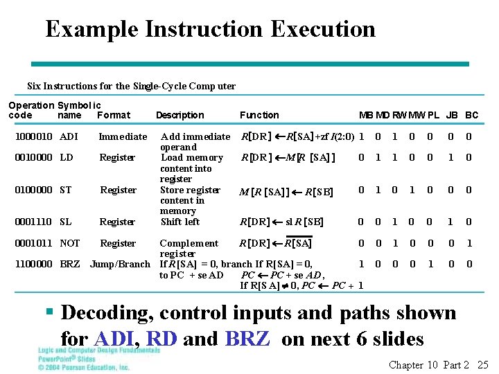
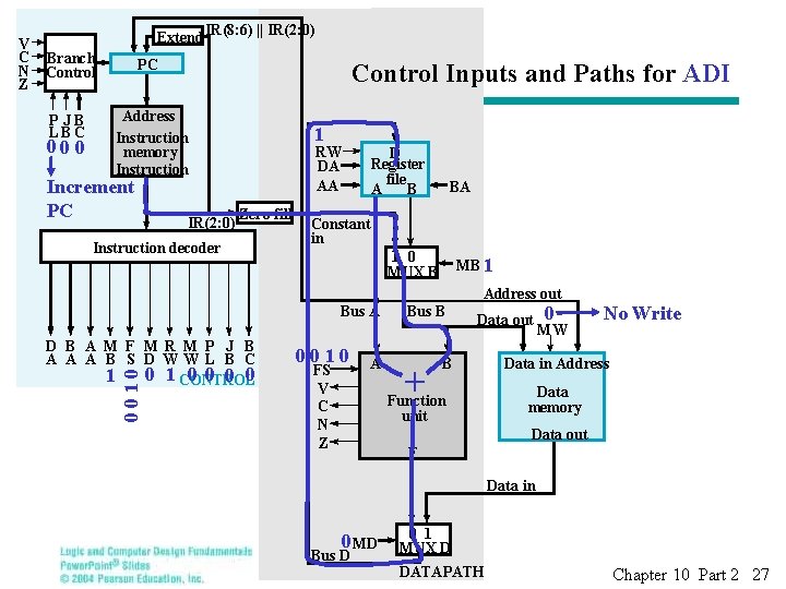
Example Instruction Execution Six Instructions for the Single-Cycle Comp uter Operation Symbol ic code name Format 1000010 ADI Imme diate 0010000 LD Register 0100000 ST Register 0001110 SL Register Description Function Add immediate R [DR ] ¬ R[SA] +zf I(2: 0) operand Load memory R [DR ] ¬ M [R [SA] ] content into register Store register M [R [SA] ] ¬ R [SB] content in memory Shift left R [DR ] ¬ sl R [SB] MB MD RW MW PL JB BC 1 0 0 0 1 1 0 0 0 1 0 Comple ment R [DR ] ¬ R [SA] 0 register 1100000 BRZ Jump/Branch If R [SA] = 0, branch If R[SA] = 0, 1 to PC + se AD PC ¬ PC + se AD , If R[S A] ¹ 0, PC ¬ PC + 1 0 0 0001011 NOT Register § Decoding, control inputs and paths shown for ADI, RD and BRZ on next 6 slides Chapter 10 Part 2 25

Decoding for ADI Instruction 1 0 0 1 0 Opcode 15 14 13 12 11 10 9 19– 17 16– 14 DA AA DR 8– 6 13– 11 10 BA 9– 6 SA 5– 3 5 1 0010 0 MB FS SB 2– 0 4 1 3 2 0 0 1 0 0 0 MD RW MW PL JB BC Control word Chapter 10 Part 2 26

Branch Control PC P JB LBC Address Instruction memory Instruction 00 0 Increment PC IR(8: 6) || IR(2: 0) Control Inputs and Paths for ADI IR(2: 0) 1 RW DA AA Zero fill Instruction decoder D Register file A B BA Constant in 1 0 MUX B MB 1 Address out Bus A D B A M F M R M P J B A A A B S D WW L B C 0 0 1 0 1 CONTROL 0010 V C N Z Extend 0010 FS V C N Z A Bus B + Data out B Function unit 0 MW No Write Data in Address Data memory Data out F Data in 0 MD Bus D 0 1 MUX D DATAPATH Chapter 10 Part 2 27

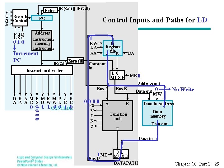
Decoding for LD Instruction 0 0 1 0 0 Opcode 15 14 13 12 11 10 9 19– 17 16– 14 DA AA DR 8– 6 13– 11 10 BA 9– 6 SA 5– 3 5 0 0000 1 MB FS SB 2– 0 4 1 3 2 0 0 1 1 0 0 MD RW MW PL JB BC Control word Chapter 10 Part 2 28

Branch Control PC P JB LBC Address Instruction memory Instruction 01 0 Increment PC IR(8: 6) || IR(2: 0) Control Inputs and Paths for LD IR(2: 0) 1 RW DA AA Zero fill Instruction decoder D Register file A B BA Constant in 1 0 MUX B MB 0 Address out Bus A D B A M F M R M P J B A A A B S D WW L B C 0 0 1 1 CONTROL 0000 V C N Z Extend 0000 FS V C N Z Bus B A Data out B Function unit 0 MW No Write Data in Address Data memory Data out F Data in 1 MD Bus D 0 1 MUX D DATAPATH Chapter 10 Part 2 29

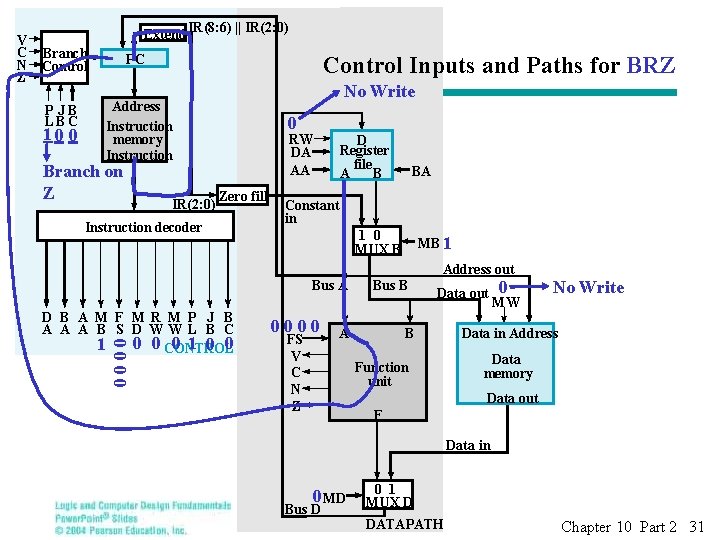
Decoding for BRZ Instruction 11 0 0 0 Opcode 15 14 13 12 11 10 9 19– 17 16– 14 DA AA DR 8– 6 13– 11 10 BA 9– 6 SA 5– 3 5 1 0000 0 MB FS SB 2– 0 4 0 3 2 0 1 1 0 0 0 MD RW MW PL JB BC Control word Chapter 10 Part 2 30

Branch Control PC P JB LBC Address Instruction memory Instruction 10 0 Branch on Z IR(8: 6) || IR(2: 0) Control Inputs and Paths for BRZ IR(2: 0) No Write 0 RW DA AA Zero fill Instruction decoder D Register file A B BA Constant in 1 0 MUX B MB 1 Address out Bus A D B A M F M R M P J B A A A B S D WW L B C 0 1 0 0 CONTROL 0000 V C N Z Extend 0000 FS V C N Z Bus B A Data out B Function unit 0 MW No Write Data in Address Data memory Data out F Data in 0 MD Bus D 0 1 MUX D DATAPATH Chapter 10 Part 2 31

Terms of Use § © 2004 by Pearson Education, Inc. All rights reserved. § The following terms of use apply in addition to the standard Pearson Education Legal Notice. § Permission is given to incorporate these materials into classroom presentations and handouts only to instructors adopting Logic and Computer Design Fundamentals as the course text. § Permission is granted to the instructors adopting the book to post these materials on a protected website or protected ftp site in original or modified form. All other website or ftp postings, including those offering the materials for a fee, are prohibited. § You may not remove or in any way alter this Terms of Use notice or any trademark, copyright, or other proprietary notice, including the copyright watermark on each slide. § Return to Title Page Chapter 10 Part 2 32

ﺍﻟﻤﻤﻠﻜﺔ ﺍﻟﻌﺮﺑﻴﺔ ﺍﻟﺴﻌﻮﺩﻳﺔ ﻭﺯﺍﺭﺓ ﺍﻟﺘﻌﻠﻴﻢ ﺟﺎﻣﻌﺔ ﺃﻢ ﺍﻟﻘﺮﻯ ﺍﻟﻜﻠﻴﺔ ﺍﻟﺠﺎﻣﻌﻴﺔ ﺃﻀﻢ ﻗﺴﻢ ﺍﻟﺤﺎﺳﺐ ﺍﻵﻠﻲ Kingdom of Saudi Arabia Ministry of Education Umm Al. Qura University Adam University College Computer Science Department This Summary is an Online Content from this Book: Morris Mano, DIGITAL DESIGN, 4 th Edition, Prentice Hall, 2007 It is edited for Logic Analysis and Design Course 6803213 -3 by: T. Mariah Sami Khayat Teacher Assistant @ Adam University College For Contacting: mskhayat@uqu. edu. sa Chapter 1 33