Logic and Computer Design Fundamentals Chapter 10 Computer

- Slides: 29

Logic and Computer Design Fundamentals Chapter 10 – Computer Design Basics Part 1 – Datapaths Charles Kime & Thomas Kaminski © 2004 Pearson Education, Inc. Terms of Use (Hyperlinks are active in View Show mode)

Overview § Part 1 – Datapaths • • • Introduction Datapath Example Arithmetic Logic Unit (ALU) Shifter Datapath Representation Control Word § Part 2 – A Simple Computer • Instruction Set Architecture (ISA) • Single-Cycle Hardwired Control § Instruction Decoder § Sample Instructions § Single Cycle Computer Issues • Multiple Cycle Hardwired Control § Sequential Control Design 2

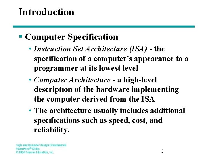
Introduction § Computer Specification • Instruction Set Architecture (ISA) - the specification of a computer's appearance to a programmer at its lowest level • Computer Architecture - a high-level description of the hardware implementing the computer derived from the ISA • The architecture usually includes additional specifications such as speed, cost, and reliability. 3

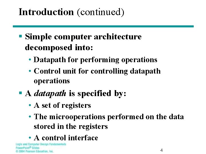
Introduction (continued) § Simple computer architecture decomposed into: • Datapath for performing operations • Control unit for controlling datapath operations § A datapath is specified by: • A set of registers • The microoperations performed on the data stored in the registers • A control interface 4

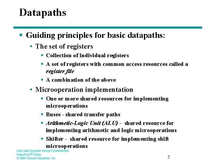
Datapaths § Guiding principles for basic datapaths: • The set of registers § Collection of individual registers § A set of registers with common access resources called a register file § A combination of the above • Microoperation implementation § One or more shared resources for implementing microoperations § Buses - shared transfer paths § Arithmetic-Logic Unit (ALU) - shared resource for implementing arithmetic and logic microoperations § Shifter - shared resource for implementing shift microoperations 5

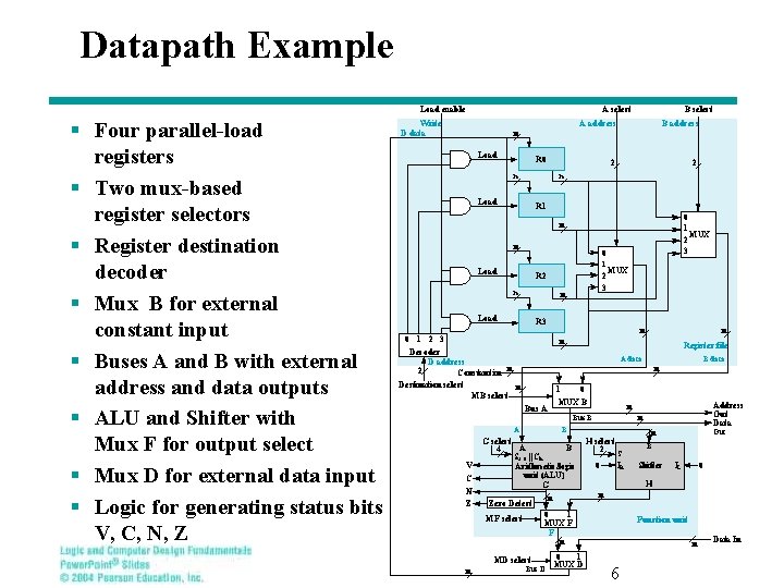
Datapath Example Load enable § Four parallel-load registers § Two mux-based register selectors § Register destination decoder § Mux B for external constant input § Buses A and B with external address and data outputs § ALU and Shifter with Mux F for output select § Mux D for external data input § Logic for generating status bits V, C, N, Z A select Write D data n Load A address B address 2 2 R 0 n B select n Load R 1 0 1 MUX 2 3 n n 0 1 Load 2 3 R 2 n n Load MUX R 3 n 0 1 2 3 n n Decoder D address 2 Constant in n Destination select n MB select Register file A data 1 0 MUX B Bus A A n C N Z B G select A B 4 S 2: 0 || Cin Arithmetic/logic unit (ALU) G MD select Bus D Out n B Shifter IL 0 H 0 1 MUX F F n MF select n H select 2 S IR 0 n n Zero Detect Address Out Data n Bus B V B data n 0 1 MUX D Function unit n 6 Data In

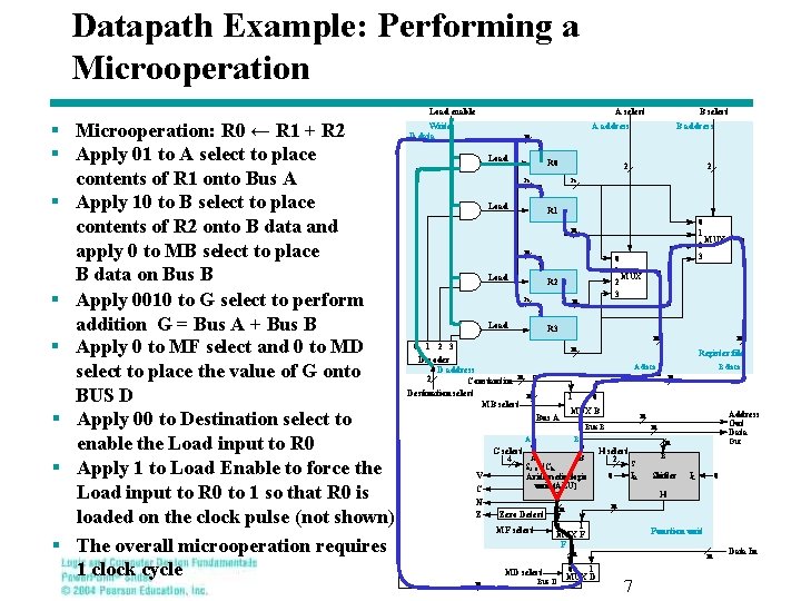
Datapath Example: Performing a Microoperation Load enable § Microoperation: R 0 ← R 1 + R 2 § Apply 01 to A select to place contents of R 1 onto Bus A § Apply 10 to B select to place contents of R 2 onto B data and apply 0 to MB select to place B data on Bus B § Apply 0010 to G select to perform addition G = Bus A + Bus B § Apply 0 to MF select and 0 to MD select to place the value of G onto BUS D § Apply 00 to Destination select to enable the Load input to R 0 § Apply 1 to Load Enable to force the Load input to R 0 to 1 so that R 0 is loaded on the clock pulse (not shown) § The overall microoperation requires 1 clock cycle A select Write D data n Load A address B address 2 2 R 0 n B select n Load R 1 0 1 MUX 2 3 n n 0 1 Load 2 3 R 2 n n Load MUX R 3 n 0 1 2 3 n n Decoder D address 2 Constant in n Destination select n MB select Register file A data 1 0 MUX B Bus A A n C N Z B G select A B 4 S 2: 0 || Cin Arithmetic/logic unit (ALU) G MD select Bus D Out n B Shifter IL 0 H 0 1 MUX F F n MF select n H select 2 S IR 0 n n Zero Detect Address Out Data n Bus B V B data n 0 1 MUX D Function unit n 7 Data In

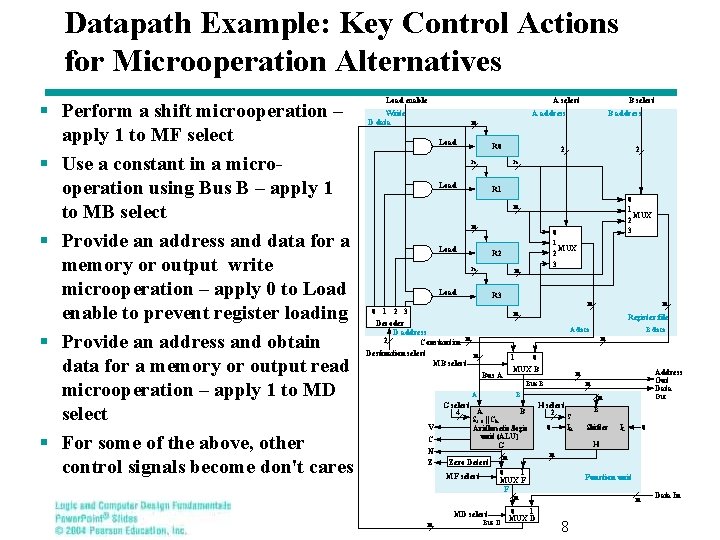
Datapath Example: Key Control Actions for Microoperation Alternatives § Perform a shift microoperation – apply 1 to MF select § Use a constant in a microoperation using Bus B – apply 1 to MB select § Provide an address and data for a memory or output write microoperation – apply 0 to Load enable to prevent register loading § Provide an address and obtain data for a memory or output read microoperation – apply 1 to MD select § For some of the above, other control signals become don't cares Load enable A select Write D data n Load A address B address 2 2 R 0 n B select n Load R 1 0 1 MUX 2 3 n n 0 1 Load 2 3 R 2 n n Load MUX R 3 n 0 1 2 3 n n Decoder D address 2 Constant in n Destination select n MB select Register file A data 1 0 MUX B Bus A A n C N Z B G select A B 4 S 2: 0 || Cin Arithmetic/logic unit (ALU) G MD select Bus D Out n B Shifter IL 0 H 0 1 MUX F F n MF select n H select 2 S IR 0 n n Zero Detect Address Out Data n Bus B V B data n 0 1 MUX D Function unit n 8 Data In

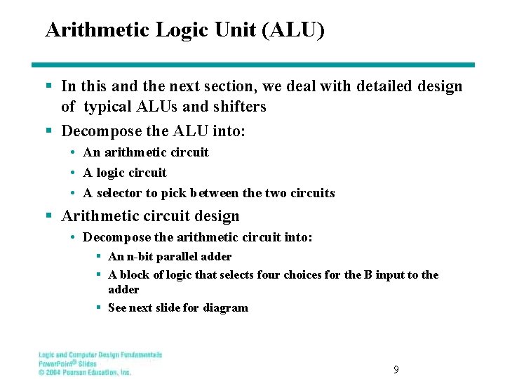
Arithmetic Logic Unit (ALU) § In this and the next section, we deal with detailed design of typical ALUs and shifters § Decompose the ALU into: • An arithmetic circuit • A logic circuit • A selector to pick between the two circuits § Arithmetic circuit design • Decompose the arithmetic circuit into: § An n-bit parallel adder § A block of logic that selects four choices for the B input to the adder § See next slide for diagram 9

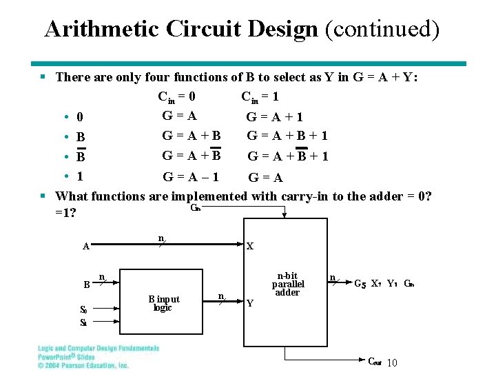
Arithmetic Circuit Design (continued) § There are only four functions of B to select as Y in G = A + Y: Cin = 0 Cin = 1 G=A+1 • 0 G=A+B+1 • B • 1 G=A– 1 G=A § What functions are implemented with carry-in to the adder = 0? Cin =1? n A B S 0 S 1 X n-bit parallel adder n B input logic n n G 5 X 1 Y 1 Cin Y Cout 10

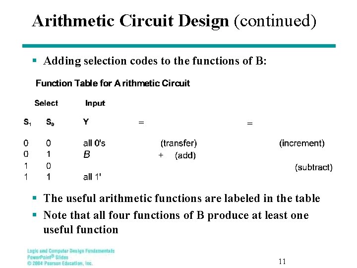
Arithmetic Circuit Design (continued) § Adding selection codes to the functions of B: = = + § The useful arithmetic functions are labeled in the table § Note that all four functions of B produce at least one useful function 11

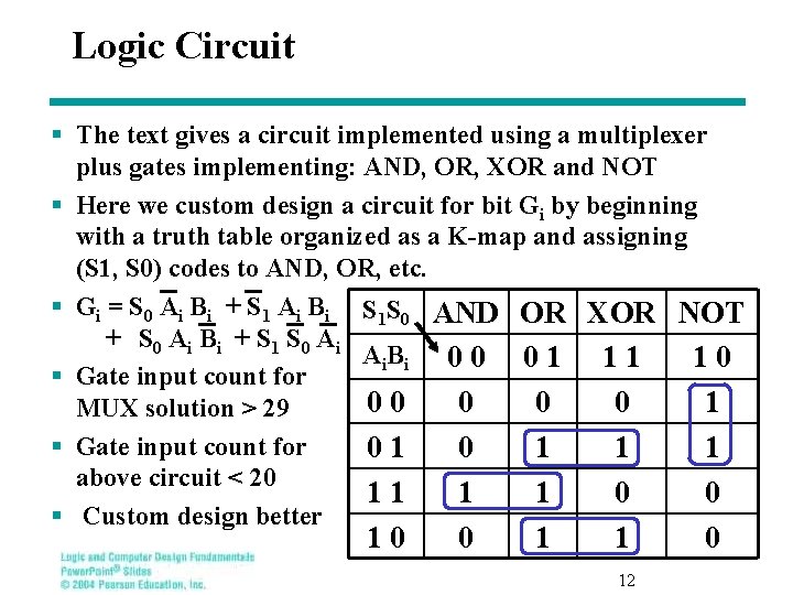
Logic Circuit § The text gives a circuit implemented using a multiplexer plus gates implementing: AND, OR, XOR and NOT § Here we custom design a circuit for bit Gi by beginning with a truth table organized as a K-map and assigning (S 1, S 0) codes to AND, OR, etc. § Gi = S 0 Ai Bi + S 1 Ai Bi S 1 S 0 AND OR XOR NOT + S 0 Ai B i + S 1 S 0 Ai Ai B i 0 0 0 1 11 10 § Gate input count for 00 0 1 MUX solution > 29 § Gate input count for 01 0 1 1 1 above circuit < 20 11 1 1 0 0 § Custom design better 10 0 1 1 12 0

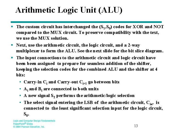
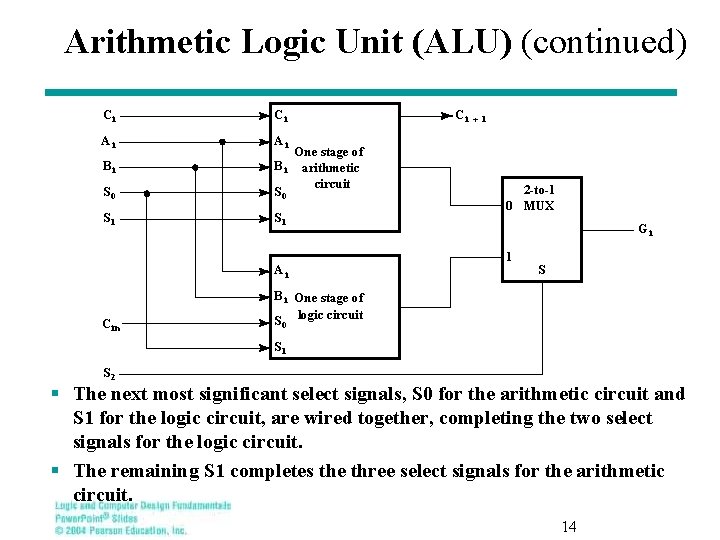
Arithmetic Logic Unit (ALU) § The custom circuit has interchanged the (S 1, S 0) codes for XOR and NOT compared to the MUX circuit. To preserve compatibility with the text, we use the MUX solution. § Next, use the arithmetic circuit, the logic circuit, and a 2 -way multiplexer to form the ALU. See the next slide for the bit slice diagram. § The input connections to the arithmetic circuit and logic circuit have been assigned to prepare for seamless addition of the shifter, keeping the selection codes for the combined ALU and the shifter at 4 bits: • Carry-in Ci and Carry-out Ci+1 go between bits • Ai and Bi are connected to both units • A new signal S 2 performs the arithmetic/logic selection • The select signal entering the LSB of the arithmetic circuit, Cin, is connected to the least significant selection input for the logic circuit, S 0. 13

Arithmetic Logic Unit (ALU) (continued) Ci Ci Ai Ai S 0 One stage of B i arithmetic circuit S 0 S 1 Bi Ai C in Ci +1 2 -to-1 0 MUX Gi 1 S B i One stage of logic circuit S 0 S 1 S 2 § The next most significant select signals, S 0 for the arithmetic circuit and S 1 for the logic circuit, are wired together, completing the two select signals for the logic circuit. § The remaining S 1 completes the three select signals for the arithmetic circuit. 14

Combinational Shifter Parameters § Direction: Left, Right § Number of positions with examples: • Single bit: § 1 position § 0 and 1 positions • Multiple bit: § 1 to n – 1 positions § 0 to n – 1 positions § Filling of vacant positions • Many options depending on instruction set • Here, will provide input lines or zero fill 15

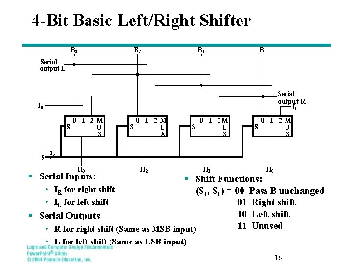
4 -Bit Basic Left/Right Shifter B 3 B 2 B 1 B 0 Serial output L Serial output R IL IR S S 0 1 2 M U X S 0 1 2 M U X 2 H 3 § Serial Inputs: H 2 H 1 H 0 § Shift Functions: • IR for right shift (S 1, S 0) = 00 Pass B unchanged • IL for left shift 01 Right shift 10 Left shift § Serial Outputs 11 Unused • R for right shift (Same as MSB input) • L for left shift (Same as LSB input) 16

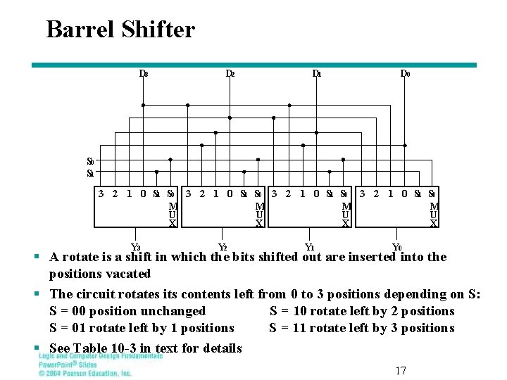
Barrel Shifter D 3 D 2 D 1 D 0 S 1 3 2 1 0 S 1 S 0 M M U U X X Y 3 Y 2 Y 1 Y 0 § A rotate is a shift in which the bits shifted out are inserted into the positions vacated § The circuit rotates its contents left from 0 to 3 positions depending on S: S = 00 position unchanged S = 10 rotate left by 2 positions S = 01 rotate left by 1 positions S = 11 rotate left by 3 positions § See Table 10 -3 in text for details 17

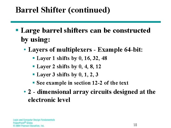
Barrel Shifter (continued) § Large barrel shifters can be constructed by using: • Layers of multiplexers - Example 64 -bit: § Layer 1 shifts by 0, 16, 32, 48 § Layer 2 shifts by 0, 4, 8, 12 § Layer 3 shifts by 0, 1, 2, 3 § See example in section 12 -2 of the text • 2 - dimensional array circuits designed at the electronic level 18

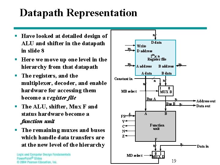
Datapath Representation § Have looked at detailed design of ALU and shifter in the datapath in slide 8 § Here we move up one level in the hierarchy from that datapath § The registers, and the multiplexer, decoder, and enable hardware for accessing them become a register file § The ALU, shifter, Mux F and status hardware become a function unit § The remaining muxes and buses which handle data transfers are at the new level of the hierarchy n D data Write D address 2 mx n Register file m m A address B address A data Constant in B data n n n 1 0 MUX B MB select Bus A FS V C N Z 4 m A n Bus B n Address out Data out B Function unit F n n MD select 0 1 MUX D 19 Data in

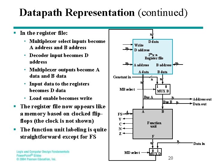
Datapath Representation (continued) § In the register file: • Multiplexer select inputs become A address and B address • Decoder input becomes D address • Multiplexer outputs become A data and B data • Input data to the registers becomes D data • Load enable becomes write § The register file now appears like a memory based on clocked flipflops (the clock is not shown) § The function unit labeling is quite straightforward except for FS n m m D data Write D address 2 mx n Register file A address B address A data Constant in B data n n n 1 0 MUX B MB select Bus A FS V C N Z 4 m A n Bus B n Address out Data out B Function unit F n n MD select 0 1 MUX D 20 Data in

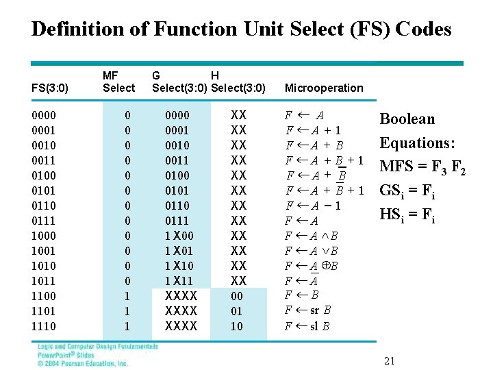
Definition of Function Unit Select (FS) Codes and MF G Select, H Select, in T FS(3: 0) 0000 0001 0010 0011 0100 0101 0110 0111 1000 1001 1010 1011 1100 1101 1110 of FS Codes MF Select 0 0 0 1 1 1 G H Select(3: 0) 0000 0001 0010 0011 0100 0101 0110 0111 1 X 00 1 X 01 1 X 10 1 X 11 XXXX XX XX XX 00 01 10 Microoperation F ¬ A F ¬A + 1 F ¬A + B + 1 F ¬A - 1 F ¬A F ¬ A ÙB F ¬ A ÚB F ¬ A ÅB F ¬A F ¬B F ¬ sr B F ¬ sl B Boolean Equations: MFS = F 3 F 2 GSi = Fi HSi = Fi 21

The Control Word § The datapath has many control inputs § The signals driving these inputs can be defined and organized into a control word § To execute a microinstruction, we apply control word values for a clock cycle. For most microoperations, the positive edge of the clock cycle is needed to perform the register load § The datapath control word format and the field definitions are shown on the next slide 22

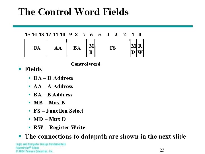
The Control Word Fields 15 14 13 12 11 10 9 8 DA § Fields • • AA 7 6 BA 5 M B 4 3 FS 2 1 0 MR D W Control word DA – D Address AA – A Address BA – B Address MB – Mux B FS – Function Select MD – Mux D RW – Register Write § The connections to datapath are shown in the next slide 23

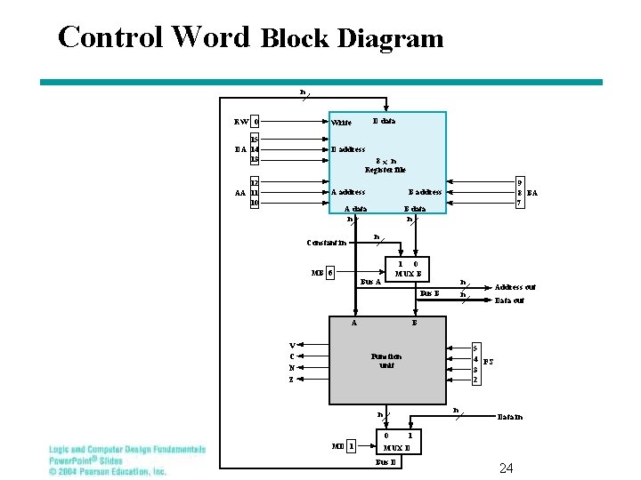
Control Word Block Diagram n D data RW 0 Write 15 DA 14 13 D address 12 AA 11 10 A address 8 x n Register file 9 8 BA 7 B address A data n B data n n Constant in MB 6 1 0 MUX B Bus A n n Bus B A V C N Z Data out B 5 4 FS 3 2 Function unit n n 0 MD 1 Address out Data in 1 MUX D Bus D 24

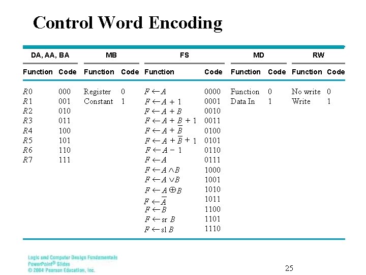
Control Word Encoding of Control W DA, AA, BA MB FS Function Code Function R 0 R 1 R 2 R 3 R 4 R 5 R 6 R 7 Register 0 Constant 1 000 001 010 011 100 101 110 111 MD Code F ¬A 0000 0001 F ¬A + 1 0010 F ¬A + B F ¬ A + B + 1 0011 F ¬A + B 0100 F ¬ A + B + 1 0101 F ¬A - 1 0110 F ¬A 0111 F ¬ A ÙB 1000 F ¬ A ÚB 1001 1010 F ¬A ÅB 1011 F ¬A 1100 F ¬B 1101 F ¬ sr B 1110 F ¬ sl B RW Function Code Function 0 Data In 1 No write 0 Write 1 25

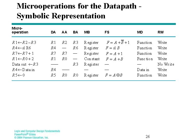
Microoperations for the Datapath Symbolic Representation Microoperation DA AA BA MB FS MD RW R 1¬R 2 –R 3 R 4 ¬ sl R 6 R 7¬R 7 + 1 R 1¬R 0 + 2 Data out ¬ R 3 R 4 ¬ Data in R 5¬ 0 R 1 R 4 R 7 R 1 —— R 4 R 5 R 2 — R 7 R 0 R 3 R 6 — — R 3 Register Re gister Con stant Register — Register F = A +B +1 F = sl B F = A +1 F = A +B — — F = A ÅB Function Func tion — Data in Function Write No Wr ite Write —— R 0 26

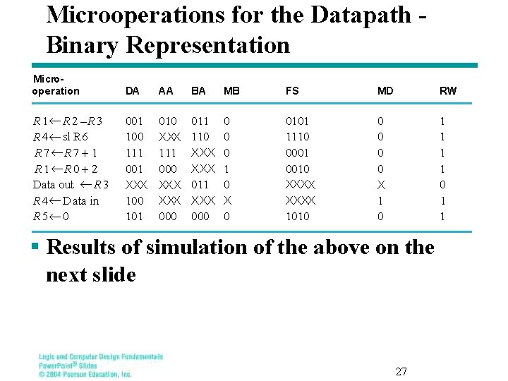
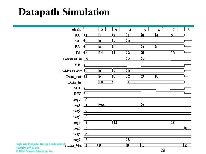
Microoperations for the Datapath Binary Representation m Microoperations from Ta Binary Co o Microoperation DA AA BA MB FS MD RW R 1¬R 2 –R 3 R 4 ¬ sl R 6 R 7¬R 7 + 1 R 1¬R 0 + 2 Data out ¬ R 3 R 4 ¬ D ata in R 5¬ 0 001 100 111 001 XXX 100 101 010 XXX 111 000 XXX 000 011 110 XXX 011 XXX 000 0 1 0 X 0 0101 1110 0001 0010 0 0 X 1 0 1 1 XXXX 1010 § Results of simulation of the above on the next slide 27

Datapath Simulation clock 2 4 3 7 4 1 2 0 7 0 BA 3 6 0 FS 5 14 1 DA 1 1 AA Constant_in X 5 0 6 4 3 0 2 X 8 7 5 10 MB Address_out 2 0 7 0 Data_out 3 6 0 2 18 Data_in 3 0 18 MD RW reg 0 reg 1 0 1 reg 2 2 reg 3 3 reg 4 4 reg 5 5 reg 6 6 reg 7 7 Status_bits 2 255 2 12 18 0 0 1 X 28

Terms of Use § © 2004 by Pearson Education, Inc. All rights reserved. § The following terms of use apply in addition to the standard Pearson Education Legal Notice. § Permission is given to incorporate these materials into classroom presentations and handouts only to instructors adopting Logic and Computer Design Fundamentals as the course text. § Permission is granted to the instructors adopting the book to post these materials on a protected website or protected ftp site in original or modified form. All other website or ftp postings, including those offering the materials for a fee, are prohibited. § You may not remove or in any way alter this Terms of Use notice or any trademark, copyright, or other proprietary notice, including the copyright watermark on each slide. § Return to Title Page 29