Logic and Computer Design Dr Sanjay P Ahuja

- Slides: 25

Logic and Computer Design Dr. Sanjay P. Ahuja, Ph. D. FIS Distinguished Professor of CIS (2010 -2014) School of Computing, UNF

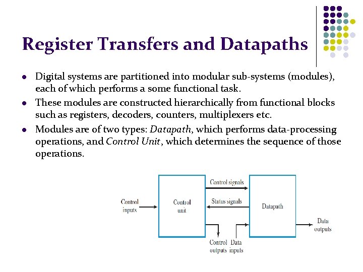
Register Transfers and Datapaths l l l Digital systems are partitioned into modular sub-systems (modules), each of which performs a some functional task. These modules are constructed hierarchically from functional blocks such as registers, decoders, counters, multiplexers etc. Modules are of two types: Datapath, which performs data-processing operations, and Control Unit, which determines the sequence of those operations.

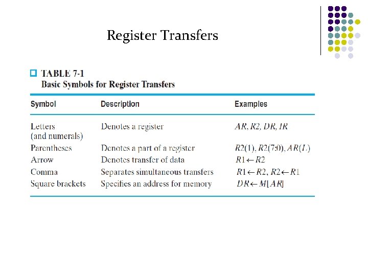
Register Transfers and Datapaths l Datapaths are defined by their registers and the operations that are performed on the data stored in the registers. l Datapath comprise of registers + ALU l The operations executed on data stored in registers are called microoperations. l Symbolic notation used to describe micro-operation transfers among registers is called a Register Transfer Language (RTL).

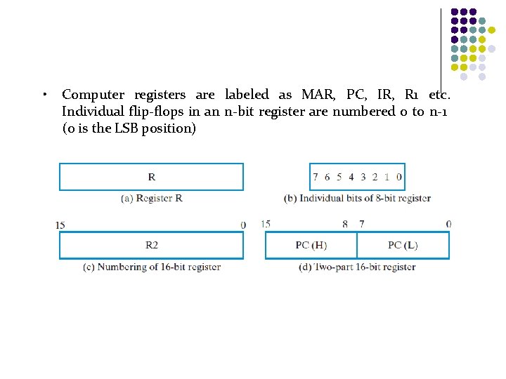
• Computer registers are labeled as MAR, PC, IR, R 1 etc. Individual flip-flops in an n-bit register are numbered 0 to n-1 (0 is the LSB position)

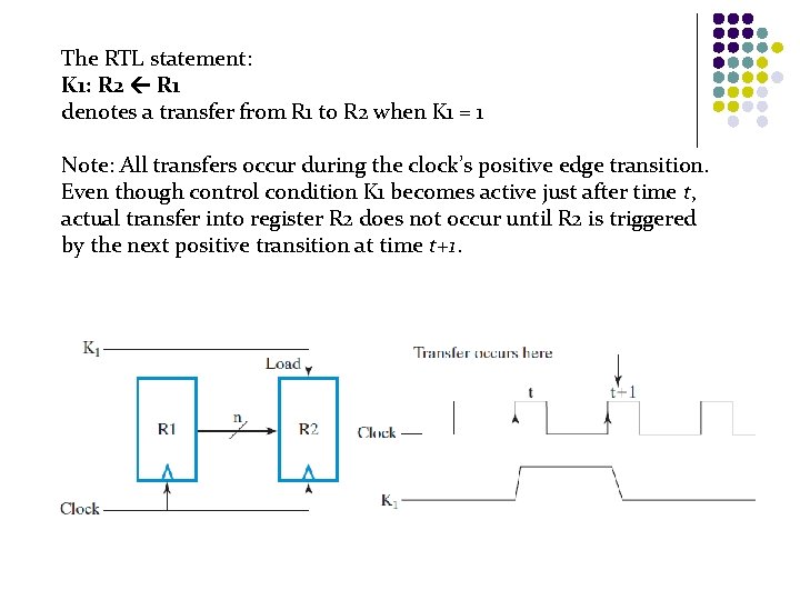
The RTL statement: K 1: R 2 R 1 denotes a transfer from R 1 to R 2 when K 1 = 1 Note: All transfers occur during the clock’s positive edge transition. Even though control condition K 1 becomes active just after time t, actual transfer into register R 2 does not occur until R 2 is triggered by the next positive transition at time t+1.

Register Transfers Using a Bus System l Since a computer has many registers, paths must be provided to transfer information from one register to another. l An efficient scheme for transferring information between registers in a multiple-register configuration is a common bus system. A bus structure consists of a set of common lines, one for each bit of a register, through which binary information is transferred one at a time. l Control signals determine which register is selected by the bus during each particular register transfer. l Bus systems can be designed using multiplexers and tri-state buffers.

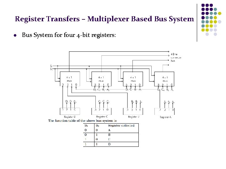
Register Transfers – Multiplexer Based Bus System l Bus System for four 4 -bit registers:

Register Transfers – Multiplexer Based Bus System l The number of multiplexers required to construct the bus is equal to n, where n is the number of bits in each register. l The size of each multiplexer must be k : 1 since it multiplexes k data lines, where k is the number of registers. l If there are 8 registers of 16 bits each, then we need 16 multiplexers, each of which is an 8 : 1 multiplexer to create the 16 bit data bus. l Disadvantage of Mux-based bus system l Mux-based bus systems may require high fan-in OR gates depending on the number of registers. In the example above we need an 8 : 1 mux since we have 8 registers to select from for the bus. Building an OR gate with such a high fan-in requires multiple levels of OR gates, introducing more logic and increasing delay. So such mux-based bus systems tend to be slower than tri-state buffer based bus systems.

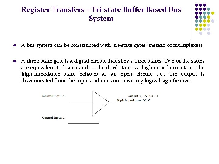
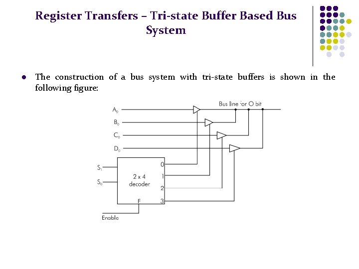
Register Transfers – Tri-state Buffer Based Bus System l A bus system can be constructed with ‘tri-state gates’ instead of multiplexers. l A three-state gate is a digital circuit that shows three states. Two of the states are equivalent to logic 1 and 0. The third state is a high impedance state. The high-impedance state behaves as an open circuit, i. e. , the output is disconnected from the input and does not have any logical significance.

Register Transfers – Tri-state Buffer Based Bus System l The construction of a bus system with tri-state buffers is shown in the following figure:

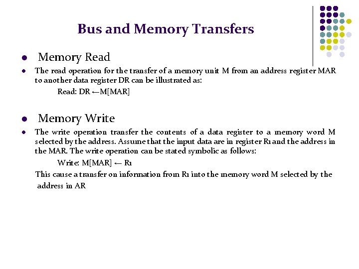
Bus and Memory Transfers l l Memory Read The read operation for the transfer of a memory unit M from an address register MAR to another data register DR can be illustrated as: Read: DR ←M[MAR] Memory Write The write operation transfer the contents of a data register to a memory word M selected by the address. Assume that the input data are in register R 1 and the address in the MAR. The write operation can be stated symbolic as follows: Write: M[MAR] ← R 1 This cause a transfer on information from R 1 into the memory word M selected by the address in AR

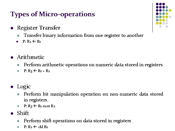
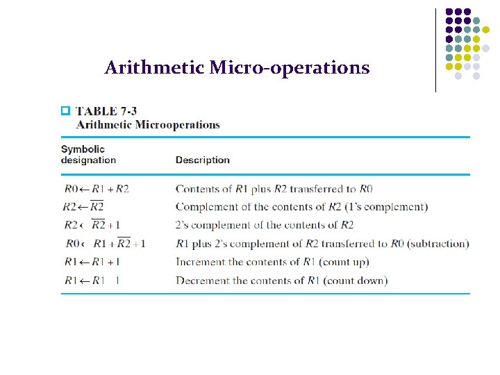
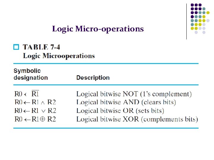
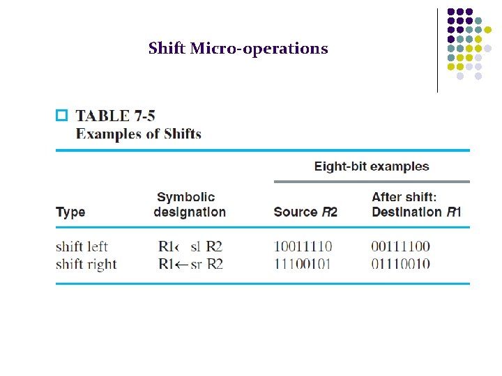
Types of Micro-operations l Register Transfer l l P: R 2 R 1 Arithmetic l Perform arithmetic operations on numeric data stored in registers l P: R 3 R 1 + R 2 Logic l l l Transfer binary information from one register to another Perform bit manipulation operation on non-numeric data stored in registers. P: R 3 R 1 exor R 2 Shift l Perform shift operations on data stored in registers l P: R 2 shl R 1

Register Transfers Fig_&_Tbl_Chapter_7. pdf - Adobe Reader

Arithmetic Micro-operations

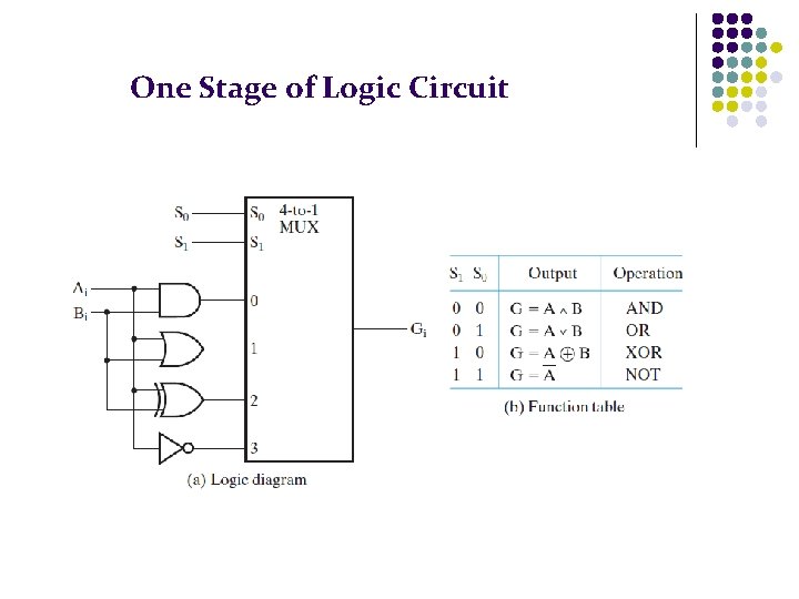
Logic Micro-operations

Shift Micro-operations

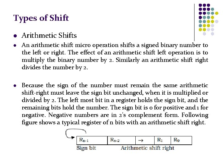
Types of Shift l Arithmetic Shifts l An arithmetic shift micro operation shifts a signed binary number to the left or right. The effect of an arithmetic shift left operation is to multiply the binary number by 2. Similarly an arithmetic shift right divides the number by 2. l Because the sign of the number must remain the same arithmetic shift-right must leave the sign bit unchanged, when it is multiplied or divided by 2. The left most bit in a register holds the sign bit, and the remaining bits hold the number. The sign bit is 0 for positive and 1 for negative. Negative numbers are in 2’s complement form. Following figure shows a typical register of n bits with an arithmetic shift right.

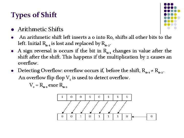
Types of Shift l l Arithmetic Shifts An arithmetic shift left inserts a 0 into R 0, shifts all other bits to the left. Initial Rn-1 is lost and replaced by Rn-2. A sign reversal is occurs if the bit in Rn-1 changes in value after the shift. This happens if the multiplication by 2 causes an overflow. Detecting Overflow: overflow occurs if, before the shift, Rn-1 ≠ Rn-2. An overflow flip-flop Vs is used to detect overflow. Vs = Rn-1 exor Rn-2

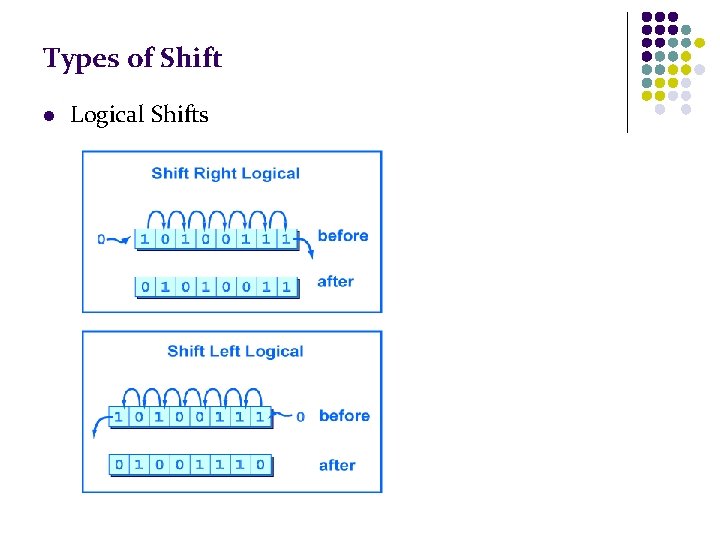
Types of Shift l Logical Shifts

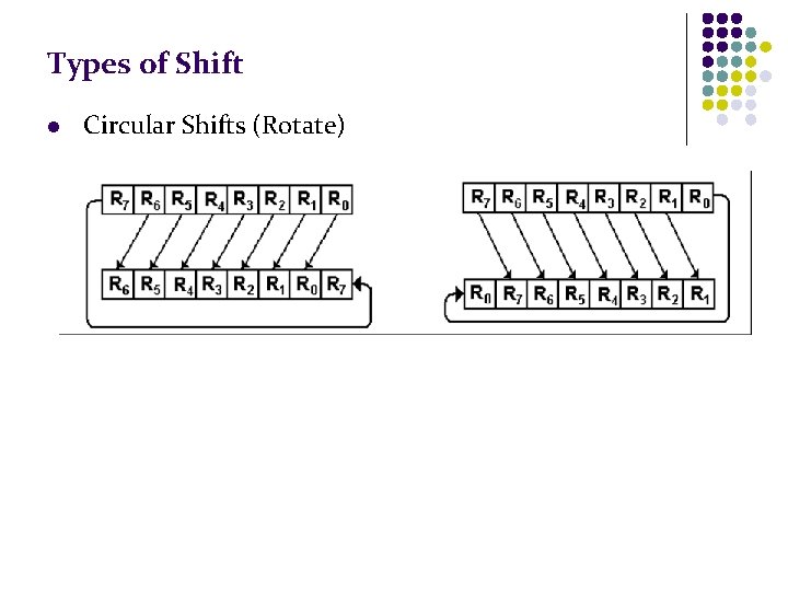
Types of Shift l Circular Shifts (Rotate)

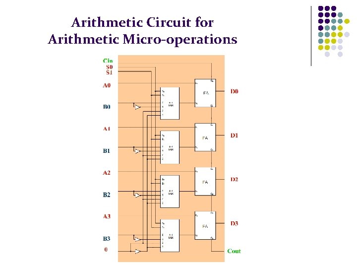
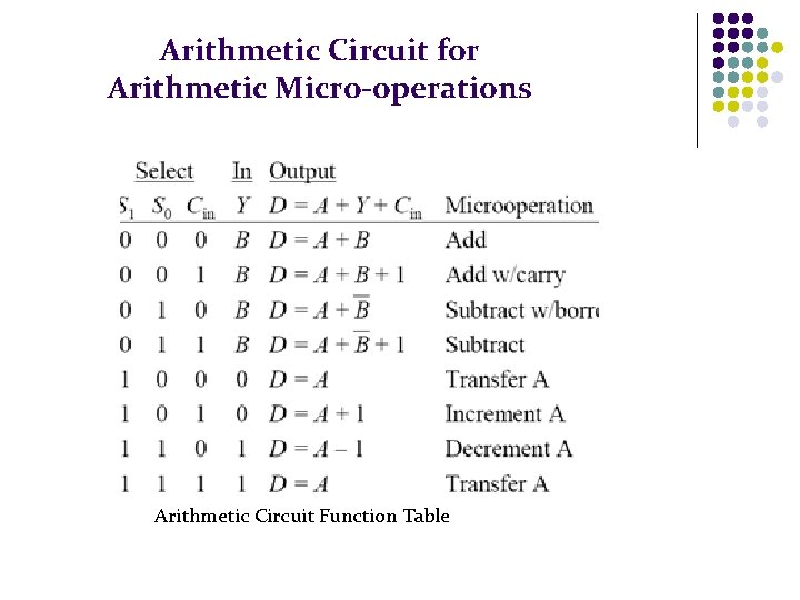
Arithmetic Circuit for Arithmetic Micro-operations

Arithmetic Circuit for Arithmetic Micro-operations Arithmetic Circuit Function Table

One Stage of Logic Circuit

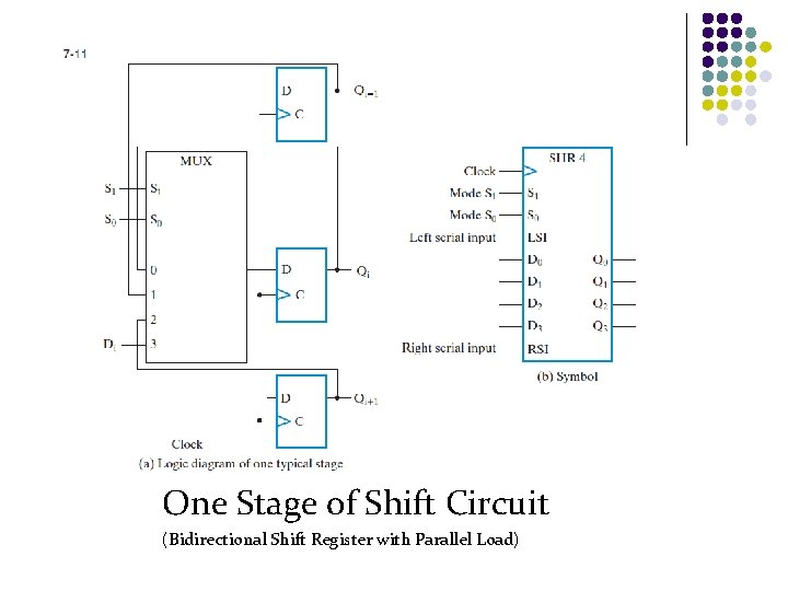
One Stage of Shift Circuit (Bidirectional Shift Register with Parallel Load)

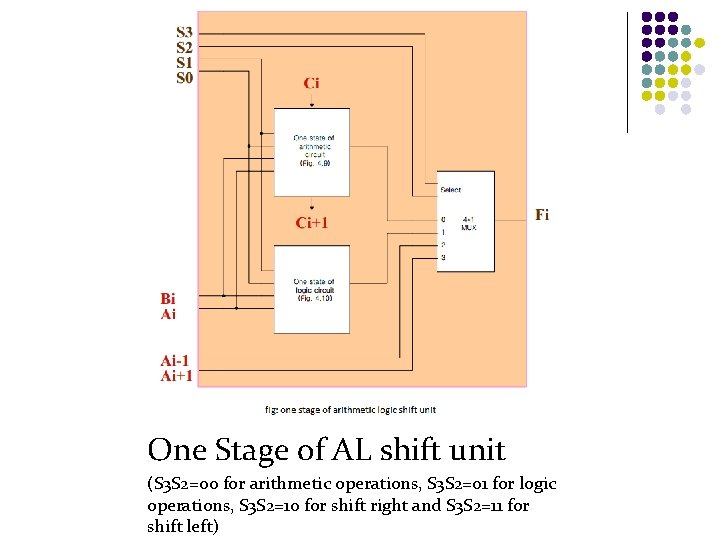
One Stage of AL shift unit (S 3 S 2=00 for arithmetic operations, S 3 S 2=01 for logic operations, S 3 S 2=10 for shift right and S 3 S 2=11 for shift left)