Log Amplifiers The basic log amplifier produces an

Log Amplifiers The basic log amplifier produces an output voltage as a function of the logarithm of the input voltage; i. e. , Vout = -K ln(Vin), where K is a constant. Recall that the a diode has an exponential characteristic up to a forward voltage of approximately 0. 7 V. Hence, the semiconductor pn junction in the form of a diode or the base emitter junction of a BJT can be used to provide a logarithm characteristic.
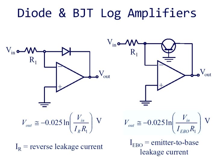

There are several applications of log and antilog amplifiers. • Antilog computation may require functions such as In x, log x or sinh x. These can be performed continuously with log-amps. • One would like to have direct d. B display on digital voltmeter and spectrum analyzer. Log-amp can easily perform this function. • Log-amp can also be used to compress the dynamic range of a signal. Log Amplifier The fundamental log-amp circuit is shown in Fig. 4. 34 (a) where a grounded base transistor is placed in the feedback path. Since the collector is held at virtual ground and the base is also grounded, the transistor's voltage-current relationship becomes that of a diode and is given by,
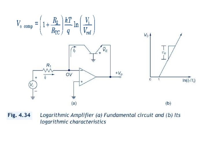

Since, IC = IE for a grounded base transistor Since IE = IC IS = emitter saturation current = 10 -13 A k = Boltzmann's Constant T = absolute temperature (in 0 K) From Fig. 4. 18(a) Taking natural Log on both sides, we get

The circuit, however, has one problem. • The emitter saturation current IS varies from transistor to transistor and with temperature. Thus a stable reference voltage Vref cannot be obtained. • This is eliminated by the circuit given in Fig. 4. 18 (b). The input is applied to one log-amp, while a reference voltage is applied to another log-amp. The two transistors are integrated close together in the same silicon wafer. This provides a close match of saturation currents and ensures good thermal tracking.

V 1 V 2 Thermistor
")
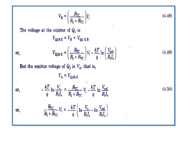
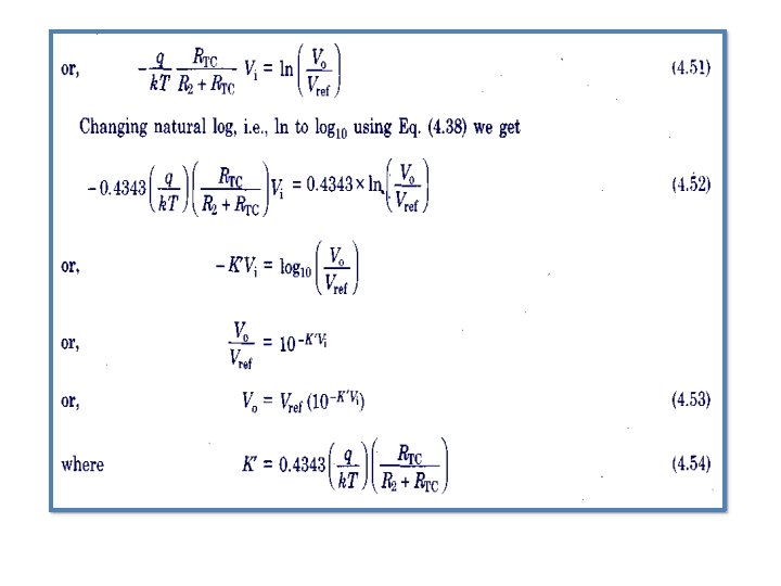
Assume, Is 1 = Is 2 = Is and then, V 1 (4. 39) = 4. 41 4. 42 4. 43 Thus reference level is now set with a single external voltage source. Its dependence on device and temperature has been removed. The voltage Vo is still dependent upon temperature and is directly proportional to T. This is compensated by the last op-amp stage A 4 which provides a non-inverting gain of (1 + R 2/RTC ). NOW, the output voltage is, 4. 44 Where RTC IS A PTC THERMISTOR.

Vin is converted in to current Ic = IEBOe. Vin/K
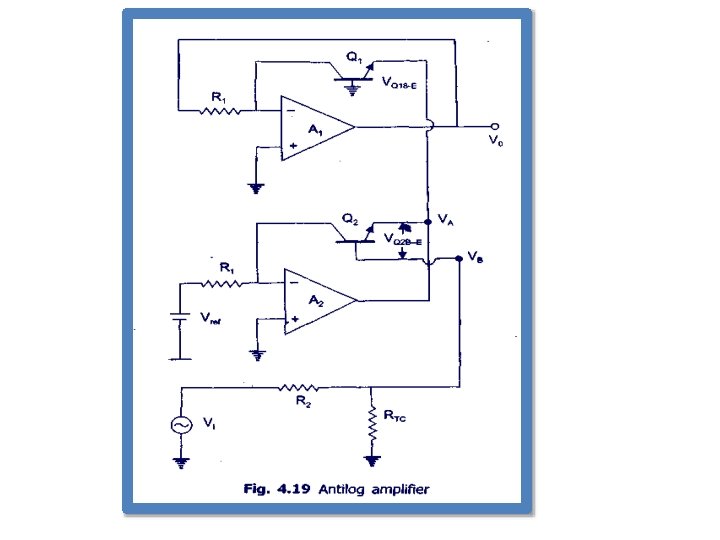

Antilog Amplifier The circuit is shown in Fig. 4. 19. The input V; for the antilog-amp is fed into the temperature compensating voltage divider R 2 and RTC and then to the base of Q 2. The output Vo of the antilog-amp is fed back to the inverting input of A 1 through the resistor R 1. The base to emitter voltage of transistors Ql and Q 2 can be written as
- Slides: 13