LLRF System RD ERL ERL LLRF System Kevin
- Slides: 6

LLRF System R&D ERL ERL LLRF System Kevin S. Smith February 17 -18, 2010

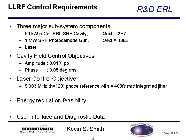
LLRF Control Requirements R&D ERL • Three major sub-system components – 50 k. W 5 -Cell ERL SRF Cavity, – 1 MW SRF Photocathode Gun, – Laser Qext = 3 E 7 Qext = 40 E 3 • Cavity Field Control Objectives – Amplitude : 0. 01% pp – Phase : 0. 05 deg rms • Laser Control Objective – 9. 383 MHz (h=120) phase reference with < 400 fs rms integrated jitter • Energy regulation feasibility • User Interface and Diagnostic Data Kevin S. Smith 2 February 17 -18, 2010

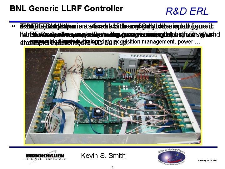
BNL Generic LLRF Controller R&D ERL R&D LLRF ERL Controller system is a stand-alone variant of theconfigurable, recently developed modular, generic • • A Two Carrier Daughter major Board Module components from which any Controller is configured: hardware LLRF Controller, / software currently platform, being the commissioned basic building block at etc. ) both from RHIC which and − Provide – “Controller” Stand alone system =control “Carrier specific system Board” functionality interface, + “Daughter (ADCs, daughter Modules” DACs, host. DSP, platform, and signal processing communication horsepower hub, acquisition management, power … athe complete EBIS injector LLRF system fortiming, RHIC isdata built up. Kevin S. Smith 3 February 17 -18, 2010

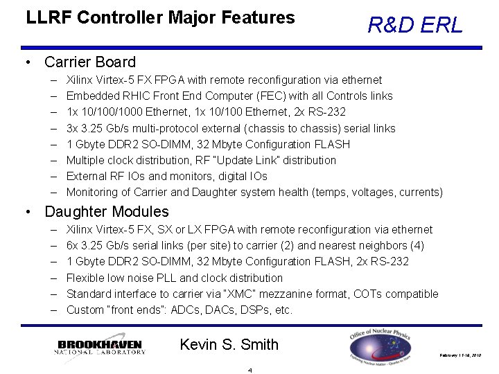
LLRF Controller Major Features R&D ERL • Carrier Board – – – – Xilinx Virtex-5 FX FPGA with remote reconfiguration via ethernet Embedded RHIC Front End Computer (FEC) with all Controls links 1 x 10/1000 Ethernet, 1 x 10/100 Ethernet, 2 x RS-232 3 x 3. 25 Gb/s multi-protocol external (chassis to chassis) serial links 1 Gbyte DDR 2 SO-DIMM, 32 Mbyte Configuration FLASH Multiple clock distribution, RF “Update Link” distribution External RF IOs and monitors, digital IOs Monitoring of Carrier and Daughter system health (temps, voltages, currents) • Daughter Modules – – – Xilinx Virtex-5 FX, SX or LX FPGA with remote reconfiguration via ethernet 6 x 3. 25 Gb/s serial links (per site) to carrier (2) and nearest neighbors (4) 1 Gbyte DDR 2 SO-DIMM, 32 Mbyte Configuration FLASH, 2 x RS-232 Flexible low noise PLL and clock distribution Standard interface to carrier via “XMC” mezzanine format, COTs compatible Custom “front ends”: ADCs, DACs, DSPs, etc. Kevin S. Smith 4 February 17 -18, 2010

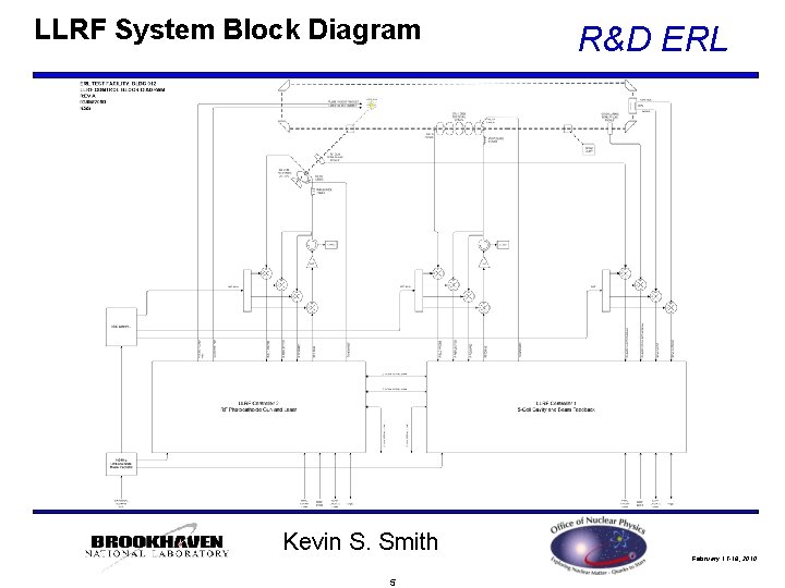
LLRF System Block Diagram Kevin S. Smith 5 R&D ERL February 17 -18, 2010

LLRF System Topology R&D ERL • System is a variant of the BNL RHIC and EBIS LLRF systems currently undergoing development and commissioning • Generator Driven Resonator − Very commonly used (CEBAF, SNS, Cornell …) − Amplitude and Phase stabilization via digital IQ control loop readily implemented in modern FPGA based systems − Intrigued by JLAB digital SEL as well − Currently characterizing 5 -cell cavity behavior using analog PLL system. • • RF DACs are 16 bit, 400 MSPS, 1 GHz analog BW RF ADCs are 16 bit, 100 MSPS, 700 MHz analog BW Current plan is to use a 96. 25 MHz IF = 800 MHz – 703. 75 MHz Systems based on similar technology have already demonstrated 0. 01% amplitude and 0. 02 deg phase stability Kevin S. Smith 6 February 17 -18, 2010