
Litografia da fascio elettronico SEM Imaging System overview
- Slides: 80
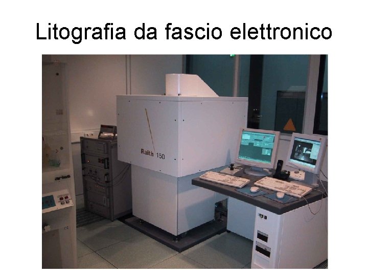
Litografia da fascio elettronico
SEM Imaging - System overview - Types of Electron Beam columns - Magnification and deflection system - Focussing (contamination dots) - Imaging
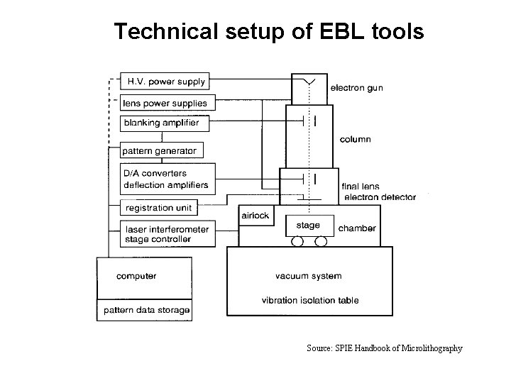
Technical setup of EBL tools Source: SPIE Handbook of Microlithography
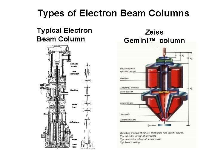
Types of Electron Beam Columns Typical Electron Beam Column Zeiss Gemini™ column
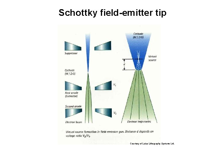
Schottky field-emitter tip Courtesy of Leica Lithography Systems Ltd.
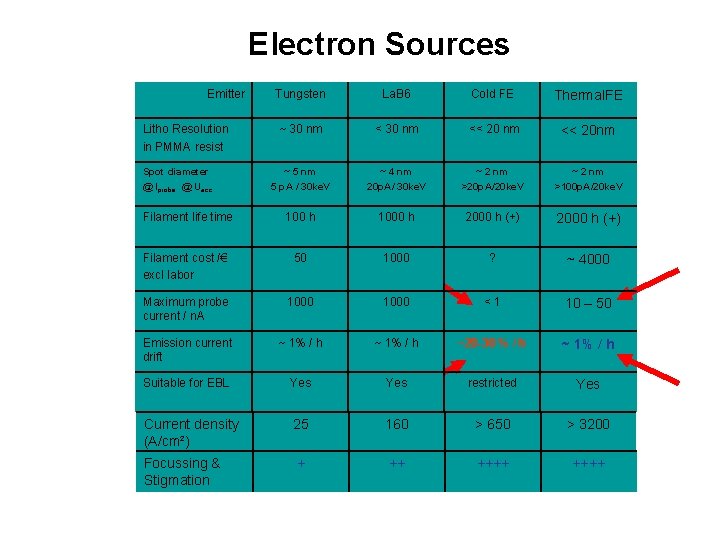
Electron Sources Tungsten La. B 6 Cold FE Thermal. FE ~ 30 nm << 20 nm ~ 5 nm 5 p. A / 30 ke. V ~ 4 nm 20 p. A/ 30 ke. V ~ 2 nm >20 p. A/20 ke. V ~ 2 nm >100 p. A/20 ke. V Filament life time 100 h 1000 h 2000 h (+) Filament cost /€ excl labor 50 1000 ? ~ 4000 Maximum probe current / n. A 1000 <1 10 – 50 Emission current drift ~ 1% / h ~20 -30 % / h ~ 1% / h Suitable for EBL Yes restricted Yes Current density (A/cm²) 25 160 > 650 > 3200 Focussing & Stigmation + ++ ++++ Emitter Litho Resolution in PMMA resist Spot diameter @ Iprobe @ Uacc
Comparison of stage specifications
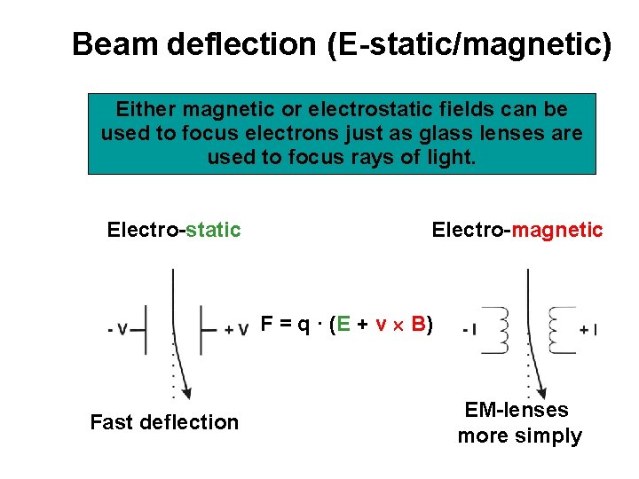
Beam deflection (E-static/magnetic) Either magnetic or electrostatic fields can be used to focus electrons just as glass lenses are used to focus rays of light. Electro-static Electro-magnetic F = q · (E + v B) Fast deflection EM-lenses more simply
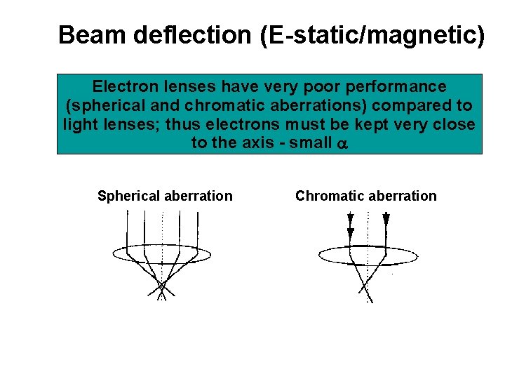
Beam deflection (E-static/magnetic) Electron lenses have very poor performance (spherical and chromatic aberrations) compared to light lenses; thus electrons must be kept very close to the axis - small Spherical aberration Chromatic aberration
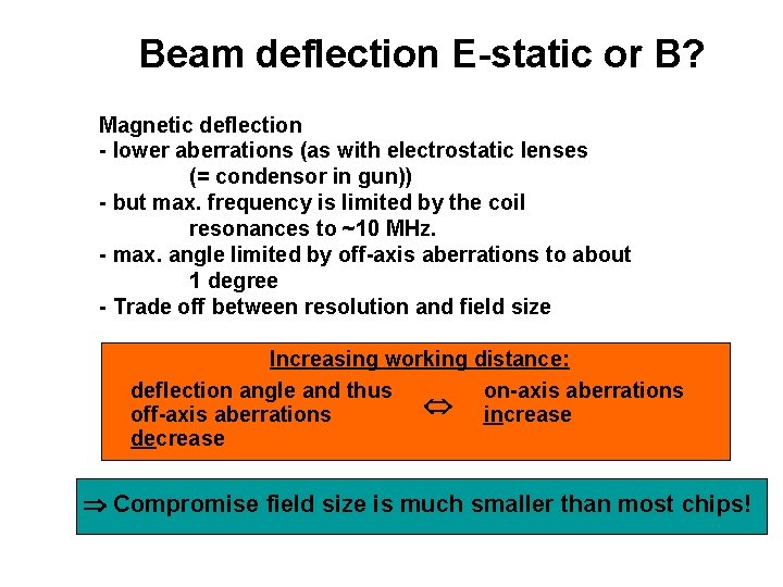
Beam deflection E-static or B? Magnetic deflection - lower aberrations (as with electrostatic lenses (= condensor in gun)) - but max. frequency is limited by the coil resonances to ~10 MHz. - max. angle limited by off-axis aberrations to about 1 degree - Trade off between resolution and field size Increasing working distance: deflection angle and thus on-axis aberrations increase off-axis aberrations decrease Compromise field size is much smaller than most chips!
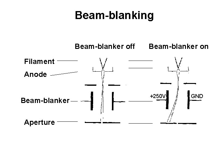
Beam-blanking Beam-blanker off Beam-blanker on Filament Anode Beam-blanker Aperture +250 V GND
Motivation To be good in EBL means to be good in SEM imaging!
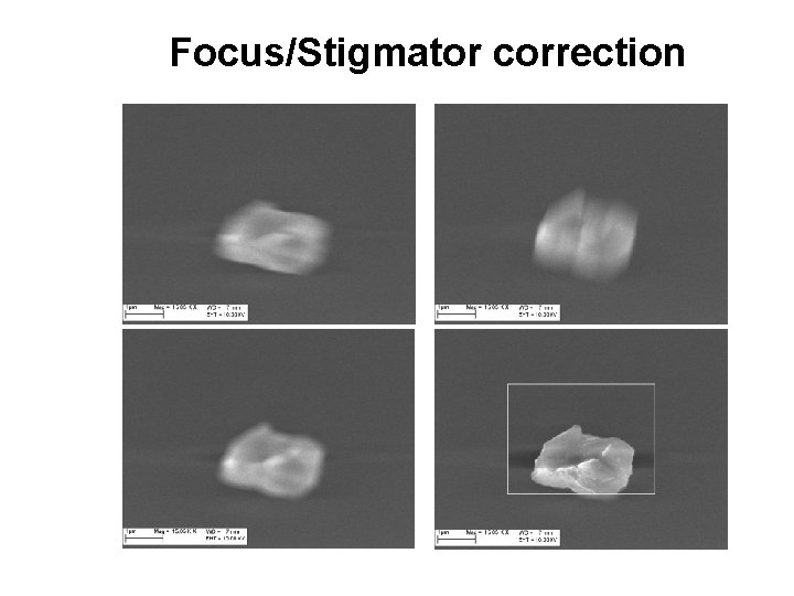
Focus/Stigmator correction
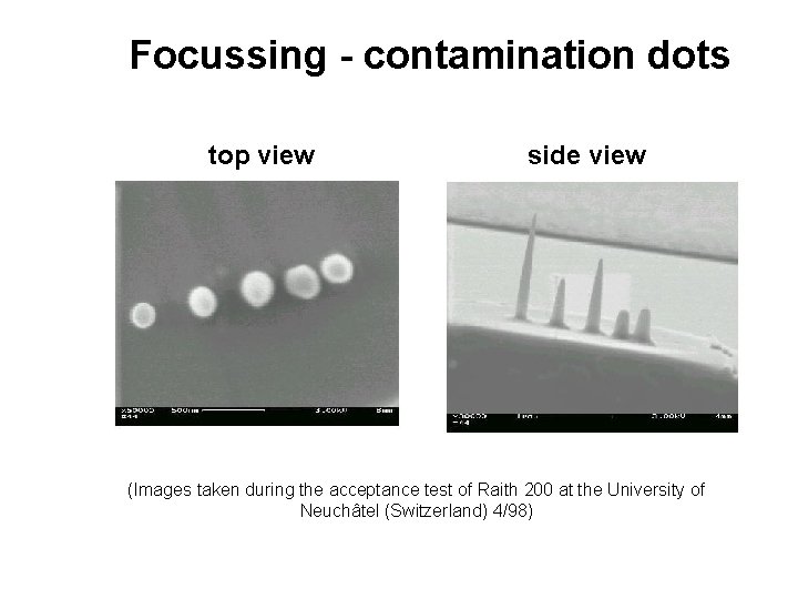
Focussing - contamination dots top view side view (Images taken during the acceptance test of Raith 200 at the University of Neuchâtel (Switzerland) 4/98)
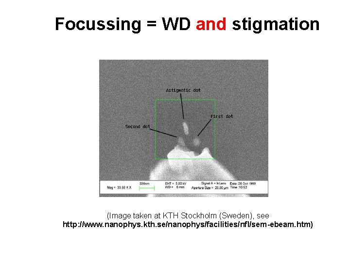
Focussing = WD and stigmation (Image taken at KTH Stockholm (Sweden), see http: //www. nanophys. kth. se/nanophys/facilities/nfl/sem-ebeam. htm)
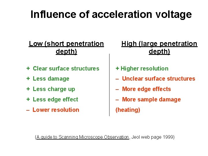
Influence of acceleration voltage Low (short penetration depth) High (large penetration depth) + Clear surface structures + Higher resolution + Less damage – Unclear surface structures + Less charge up – More edge effects + Less edge effect – More sample damage – Lower resolution (heating) (A guide to Scanning Microscope Observation, Jeol web page 1999)
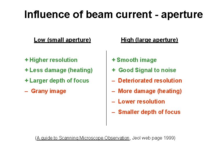
Influence of beam current - aperture Low (small aperture) High (large aperture) + Higher resolution + Smooth image + Less damage (heating) + Good Signal to noise + Larger depth of focus – Deteriorated resolution – Grany image – More damage (heating) – Lower resolution – Smaller depth of focus (A guide to Scanning Microscope Observation, Jeol web page 1999)
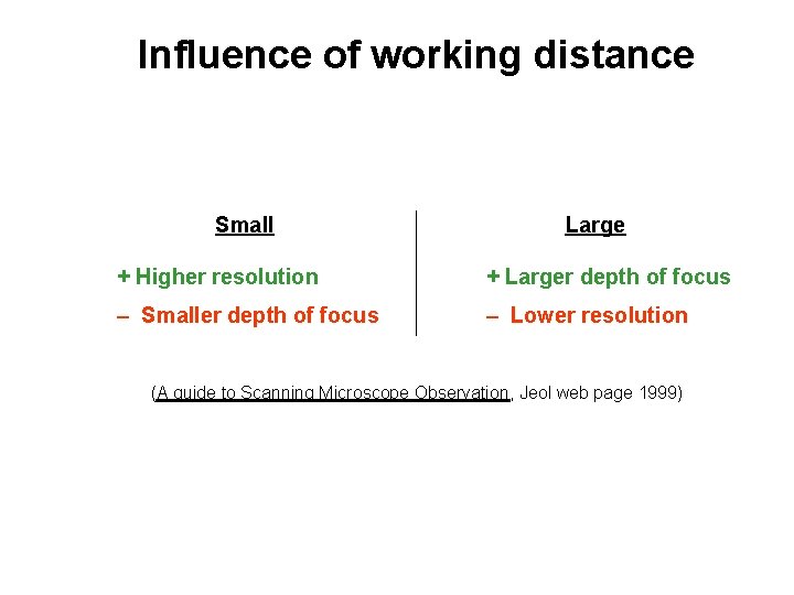
Influence of working distance Small Large + Higher resolution + Larger depth of focus – Smaller depth of focus – Lower resolution (A guide to Scanning Microscope Observation, Jeol web page 1999)
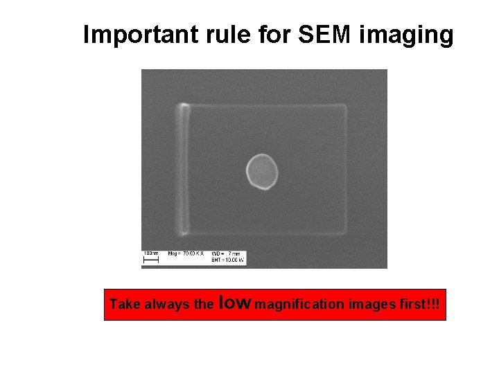
Important rule for SEM imaging Take always the low magnification images first!!!
E-Beam Lithography Methods E-beam strategies • Motivation • Stage movement strategies • EBL writing strategies
Motivation Applications of EBL • mask fabrication (e. g. chromium on glass) • direct write (rapid prototyping) • nano devices in R&D • …. different writing strategies required Recommended Literature: SPIE HANDBOOK OF MICROLITHOGRAPHY, MICROMACHINING AND MICROFABRICATION Volume 1: Microlithography, Chapter 2. 1
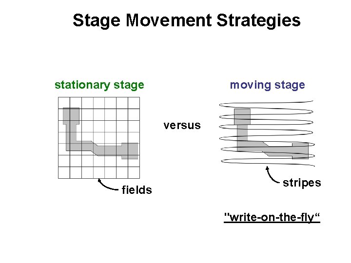
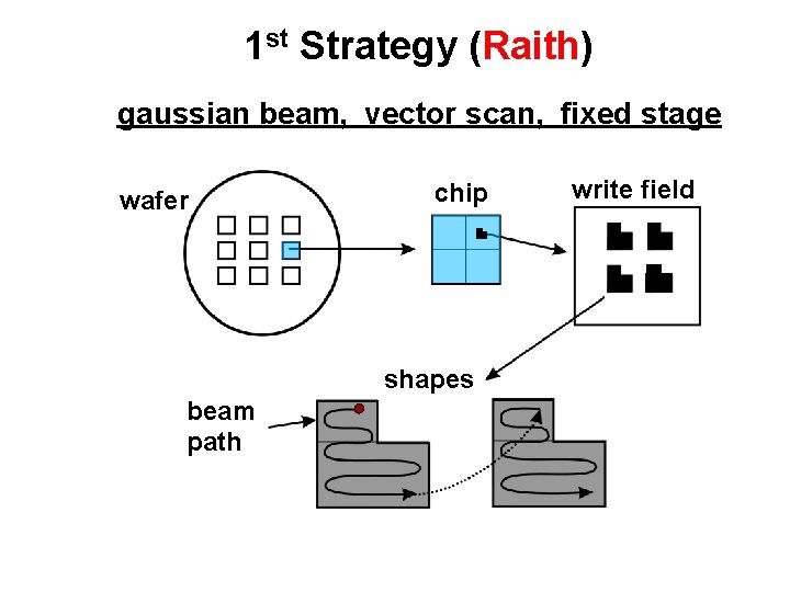
Stage Movement Strategies stationary stage moving stage versus fields stripes "write-on-the-fly“
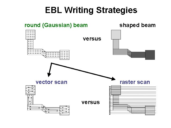
EBL Writing Strategies round (Gaussian) beam shaped beam versus vector scan raster scan versus
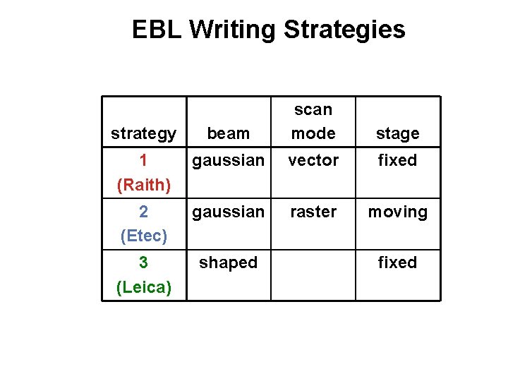
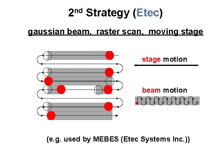
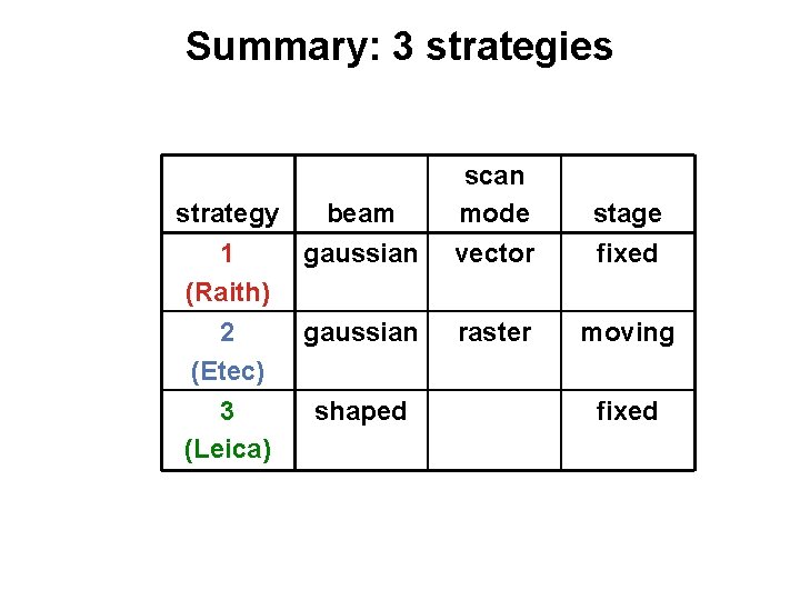
EBL Writing Strategies strategy beam scan mode 1 (Raith) gaussian vector fixed 2 (Etec) gaussian raster moving 3 (Leica) shaped stage fixed
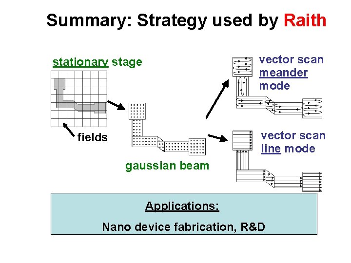
1 st Strategy (Raith) gaussian beam, vector scan, fixed stage wafer chip shapes beam path write field
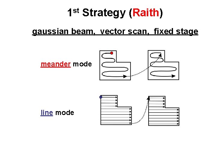
1 st Strategy (Raith) gaussian beam, vector scan, fixed stage meander mode line mode
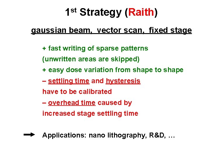
1 st Strategy (Raith) gaussian beam, vector scan, fixed stage + fast writing of sparse patterns (unwritten areas are skipped) + easy dose variation from shape to shape – settling time and hysteresis have to be calibrated – overhead time caused by increased stage settling time Applications: nano lithography, R&D, …
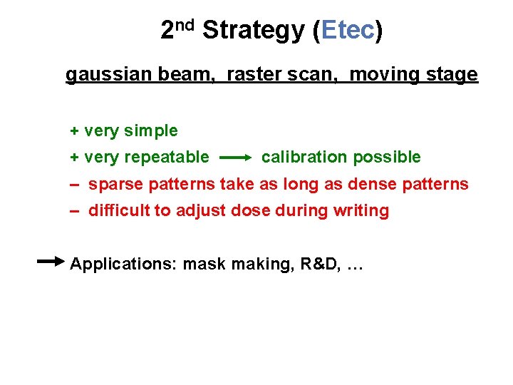
2 nd Strategy (Etec) gaussian beam, raster scan, moving stage motion beam motion (e. g. used by MEBES (Etec Systems Inc. ))
2 nd Strategy (Etec) gaussian beam, raster scan, moving stage + very simple + very repeatable calibration possible – sparse patterns take as long as dense patterns – difficult to adjust dose during writing Applications: mask making, R&D, …
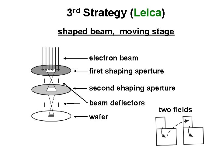
3 rd Strategy (Leica) shaped beam, moving stage electron beam first shaping aperture second shaping aperture beam deflectors wafer two fields
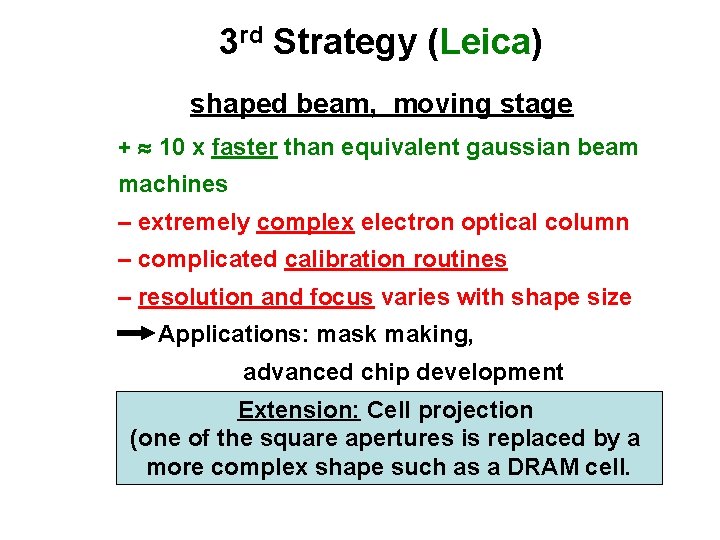
3 rd Strategy (Leica) shaped beam, moving stage + 10 x faster than equivalent gaussian beam machines – extremely complex electron optical column – complicated calibration routines – resolution and focus varies with shape size Applications: mask making, advanced chip development Extension: Cell projection (one of the square apertures is replaced by a more complex shape such as a DRAM cell.
Summary: 3 strategies strategy beam 1 gaussian (Raith) 2 gaussian (Etec) 3 shaped (Leica) scan mode vector stage fixed raster moving fixed
Summary: Strategy used by Raith vector scan meander mode stationary stage vector scan line mode fields gaussian beam Applications: Nano device fabrication, R&D
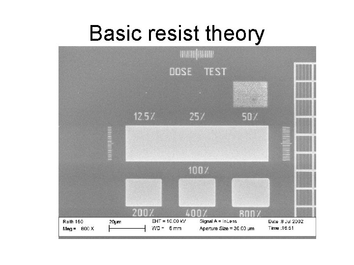
Basic resist theory
Contents • Electron scattering in resist and substrate • Proximity effect • Resist interactions (positive /negative/chemically amplified resists, resist contrast) • Dose definition • Influence of beam energy (penetration depth) • Resolution limits
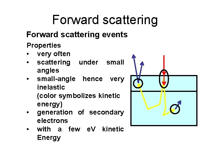
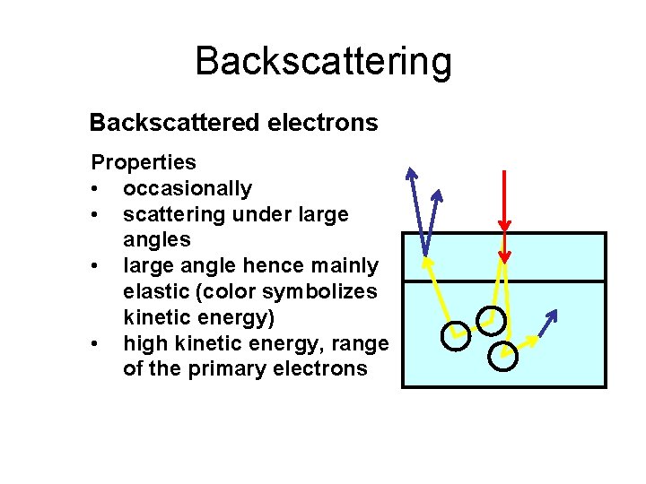
Forward scattering events Properties • very often • scattering under small angles • small-angle hence very inelastic (color symbolizes kinetic energy) • generation of secondary electrons • with a few e. V kinetic Energy
Backscattering Backscattered electrons Properties • occasionally • scattering under large angles • large angle hence mainly elastic (color symbolizes kinetic energy) • high kinetic energy, range of the primary electrons
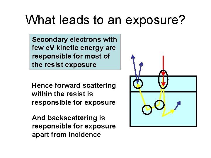
What leads to an exposure? Secondary electrons with few e. V kinetic energy are responsible for most of the resist exposure Hence forward scattering within the resist is responsible for exposure And backscattering is responsible for exposure apart from incidence
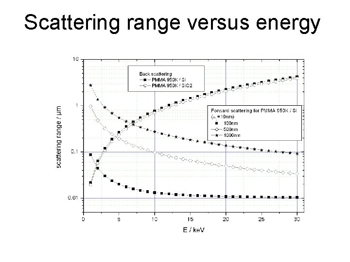
Scattering range versus energy
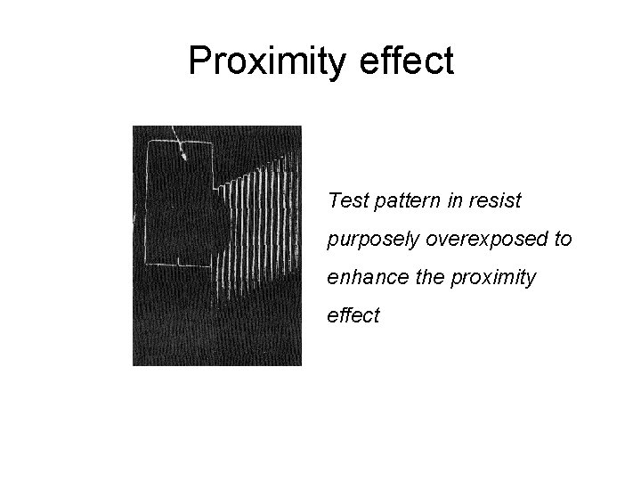
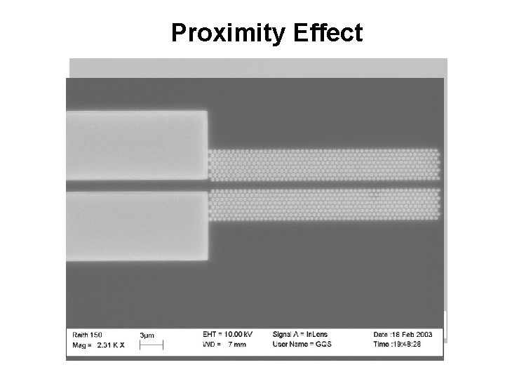
Proximity effect Test pattern in resist purposely overexposed to enhance the proximity effect
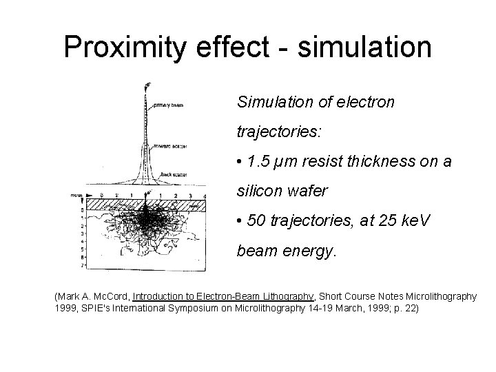
Proximity effect - simulation Simulation of electron trajectories: • 1. 5 µm resist thickness on a silicon wafer • 50 trajectories, at 25 ke. V beam energy. (Mark A. Mc. Cord, Introduction to Electron-Beam Lithography, Short Course Notes Microlithography 1999, SPIE's International Symposium on Microlithography 14 -19 March, 1999; p. 22)
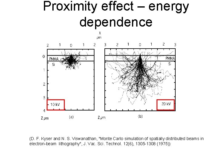
Proximity effect – energy dependence (D. F. Kyser and N. S. Viswanathan, "Monte Carlo simulation of spatially distributed beams in electron-beam lithography", J. Vac. Sci. Technol. 12(6), 1305 -1308 (1975))
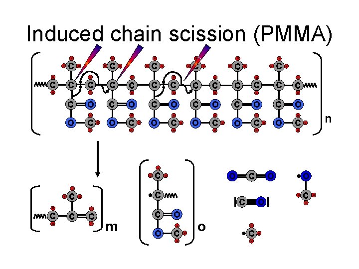
Resist interactions • Positive resists usually work by polymer chain scission; exposed polymer becomes more soluble • Negative resists usually work by cross linking between polymer chains; exposed polymer becomes insoluble
Induced chain scission (PMMA) H H C H C C H C H H C C O H C C H H O H C H C O C H O n H C O C H H H C C O C C H H C H O C H H H O C C H H H H H O O H H H C C H H O H H C H C H m C O O H C O H O C O H C H H C C C H H o O H C H H
Chemically amplified resists, are modified during exposure. However the actual exposure takes place during the post exposure bake, when the acids are activated.
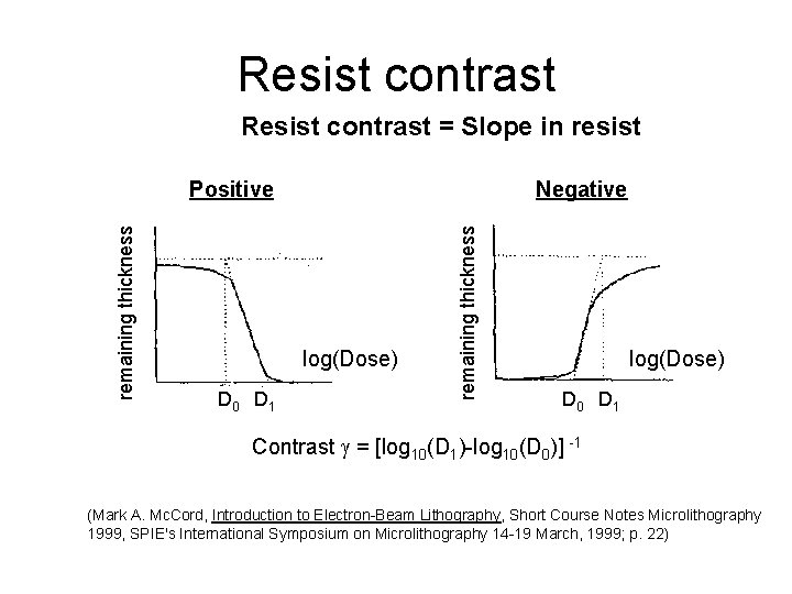
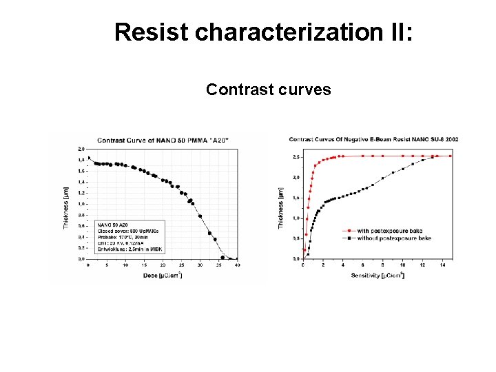
Resist contrast = Slope in resist Negative log(Dose) D 0 D 1 remaining thickness Positive log(Dose) D 0 D 1 Contrast = [log 10(D 1)-log 10(D 0)] -1 (Mark A. Mc. Cord, Introduction to Electron-Beam Lithography, Short Course Notes Microlithography 1999, SPIE's International Symposium on Microlithography 14 -19 March, 1999; p. 22)
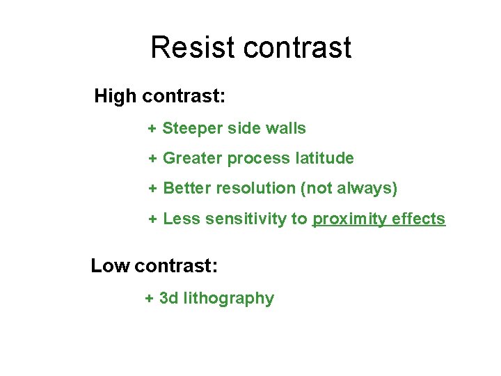
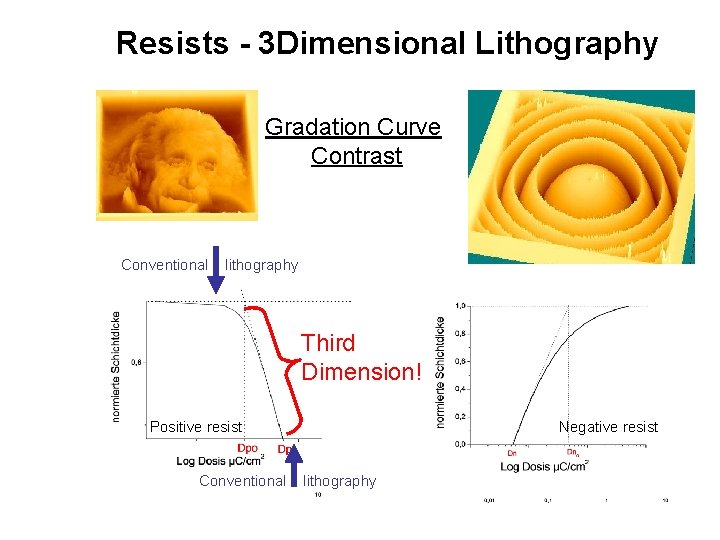
Resist contrast High contrast: + Steeper side walls + Greater process latitude + Better resolution (not always) + Less sensitivity to proximity effects Low contrast: + 3 d lithography
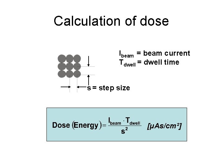
Calculation of dose Ibeam = beam current Tdwell = dwell time s = step size [µAs/cm²]
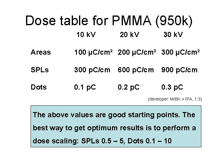
Dose table for PMMA (950 k) 10 k. V 20 k. V 30 k. V Areas 100 µC/cm² 200 µC/cm² 300 µC/cm² SPLs 300 p. C/cm 600 p. C/cm 900 p. C/cm Dots 0. 1 p. C 0. 2 p. C 0. 3 p. C (developer: MIBK + IPA, 1: 3) The above values are good starting points. The best way to get optimum results is to perform a dose scaling: SPLs 0. 5 – 5, Dots 0. 1 – 10
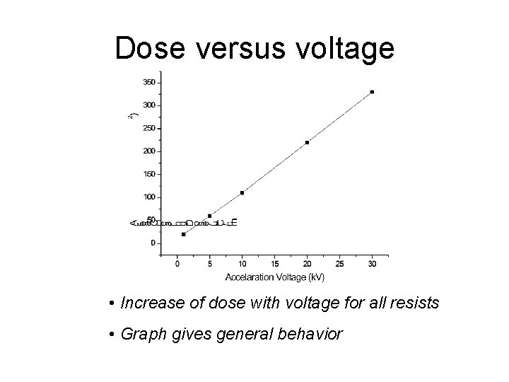
Dose versus voltage • Increase of dose with voltage for all resists • Graph gives general behavior
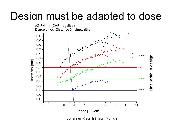
Line width in design Design must be adapted to dose Johannes Kretz, Infineon, Munich
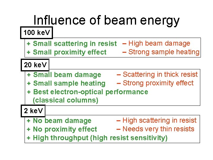
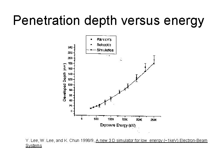
Influence of beam energy 100 ke. V + Small scattering in resist – High beam damage – Strong sample heating + Small proximity effect 20 ke. V – Scattering in thick resist + Small beam damage – Strong proximity effect + Small sample heating + Best electron-optical performance (classical columns) 2 ke. V – High scattering in resist + No beam damage – Needs very thin resists + No proximity effect + High throughput (high resist sensitivity)
Penetration depth versus energy Y. Lee, W. Lee, and K. Chun 1998/9, A new 3 D simulator for low energy (~1 ke. V) Electron-Beam Systems
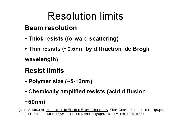
Resolution limits Beam resolution • Thick resists (forward scattering) • Thin resists (~0. 5 nm by diffraction, de Brogli wavelength) Resist limits • Polymer size (~5 -10 nm) • Chemically amplified resists (acid diffusion ~50 nm) (Mark A. Mc. Cord, Introduction to Electron-Beam Lithography, Short Course Notes Microlithography 1999, SPIE's International Symposium on Microlithography 14 -19 March, 1999; p. 63)
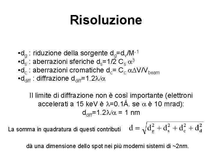
Risoluzione • dg : riduzione della sorgente dg=dv/M-1 • ds : aberrazioni sferiche ds=1/2 Cs a 3 • dc : aberrazioni cromatiche dc= Cc a. DV/Vbeam • ddiff : diffrazione ddiff=1. 2 l/a Il limite di diffrazione non è così importante (elettroni accelerati a 15 ke. V è l=0. 1Å. se a è 10 mrad): ddiff=1. 2 l/a = 1 nm La somma in quadratura di questi contributi dà una dimensione dello spot nei più moderni sistemi di ~2 nm.
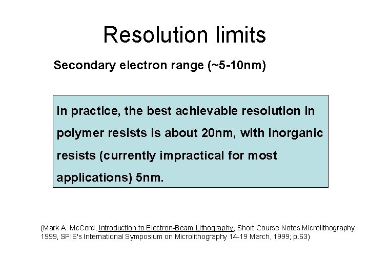
Resolution limits Secondary electron range (~5 -10 nm) In practice, the best achievable resolution in polymer resists is about 20 nm, with inorganic resists (currently impractical for most applications) 5 nm. (Mark A. Mc. Cord, Introduction to Electron-Beam Lithography, Short Course Notes Microlithography 1999, SPIE's International Symposium on Microlithography 14 -19 March, 1999; p. 63)
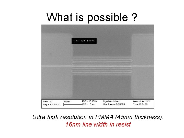
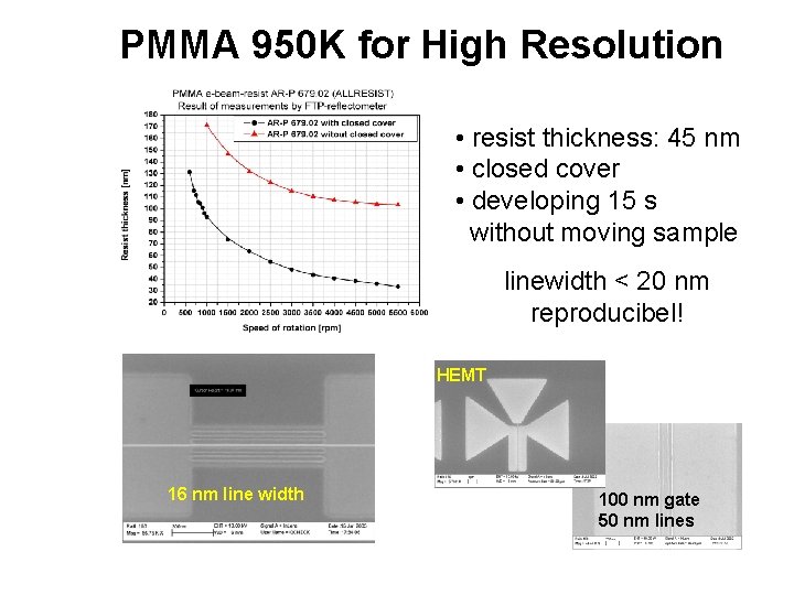
What is possible ? Ultra high resolution in PMMA (45 nm thickness): 16 nm line width in resist
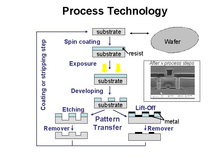
Process Technology Coating or stripping step substrate Spin coating substrate Wafer resist After x process steps Exposure substrate Developing Etching Remover substrate Pattern Transfer Lift-Off metal Remover
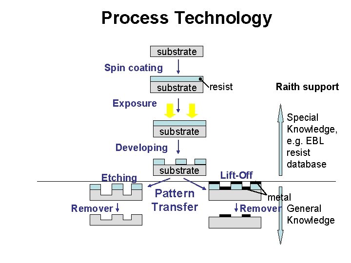
Process Technology substrate Spin coating substrate resist Raith support Exposure Special Knowledge, e. g. EBL resist database substrate Developing Etching Remover substrate Pattern Transfer Lift-Off metal Remover General Knowledge
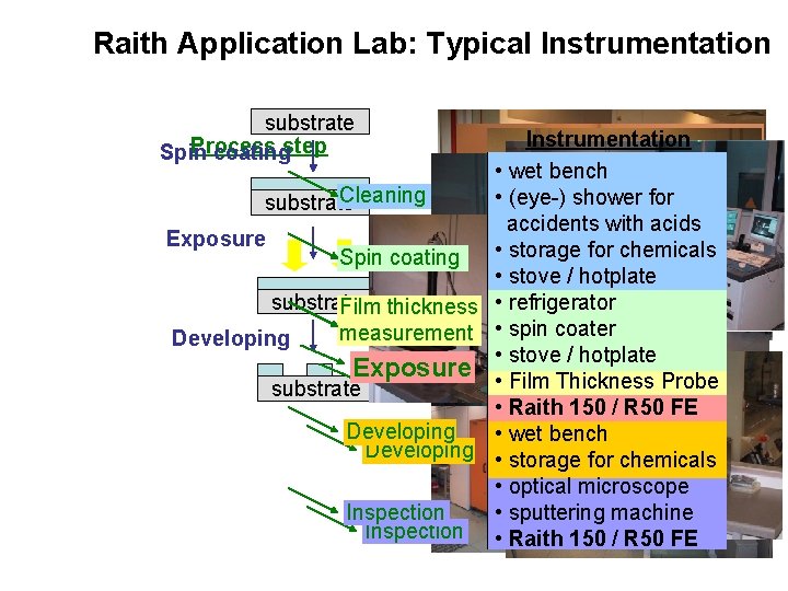
Raith Application Lab: Typical Instrumentation substrate Process Spin coatingstep Instrumentation • wet bench Cleaning • (eye-) shower for substrate accidents with acids Exposure • storage for chemicals Spin coating • stove / hotplate substrate Film thickness • refrigerator measurement • spin coater Developing • stove / hotplate Exposure • Film Thickness Probe substrate Exposure • Raith 150 / R 50 FE Developing • wet bench Developing • storage for chemicals • optical microscope Inspection • sputtering machine Inspection • Raith 150 / R 50 FE
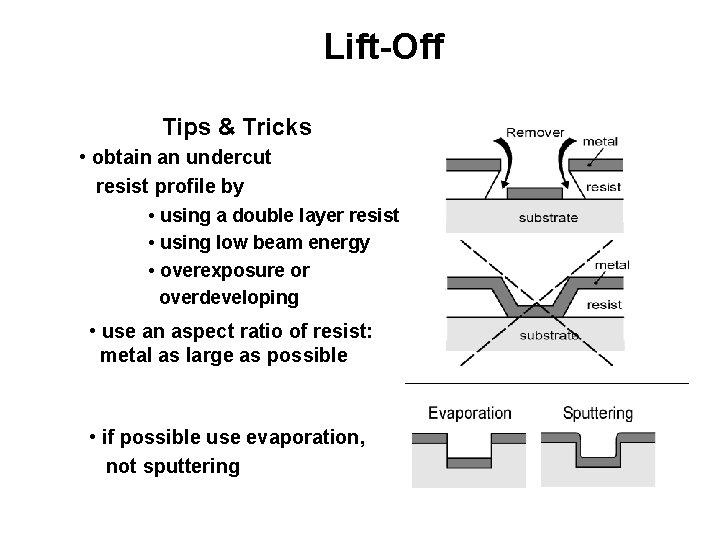
Lift-Off Tips & Tricks • obtain an undercut resist profile by • using a double layer resist • using low beam energy • overexposure or overdeveloping • use an aspect ratio of resist: metal as large as possible • if possible use evaporation, not sputtering
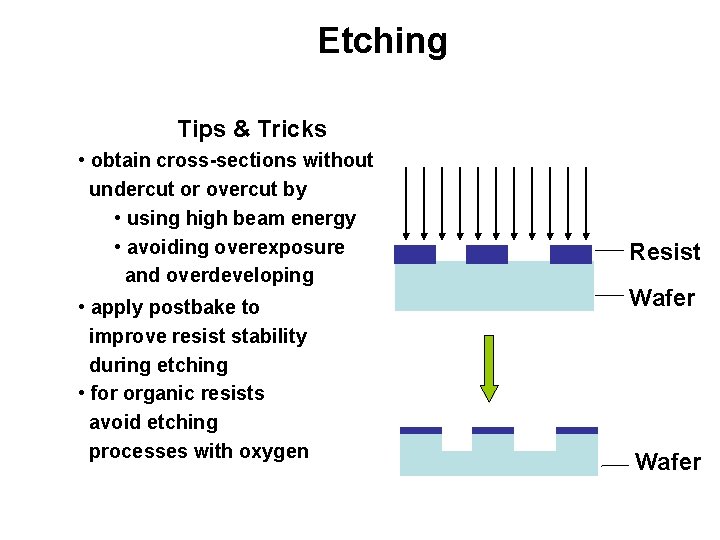
Etching Tips & Tricks • obtain cross-sections without undercut or overcut by • using high beam energy • avoiding overexposure and overdeveloping • apply postbake to improve resist stability during etching • for organic resists avoid etching processes with oxygen Resist Wafer
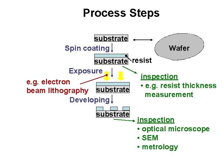
Process Steps substrate Spin coating Wafer substrate resist Exposure inspection e. g. electron • e. g. resist thickness substrate beam lithography measurement Developing substrate inspection • optical microscope • SEM • metrology
How to avoid charging effects On isolating samples an additional metal layer between resist an substrate or on top of the resist is required, e. g. • use additional Al layer on top of the resist. • thickness should be 10 nm to 20 nm • remove with KOH With an additional isolating interlayer, e. g. Si. O layer • use a higher acceleration voltage, e. g. 25 k. V for 1 µm Si. O.
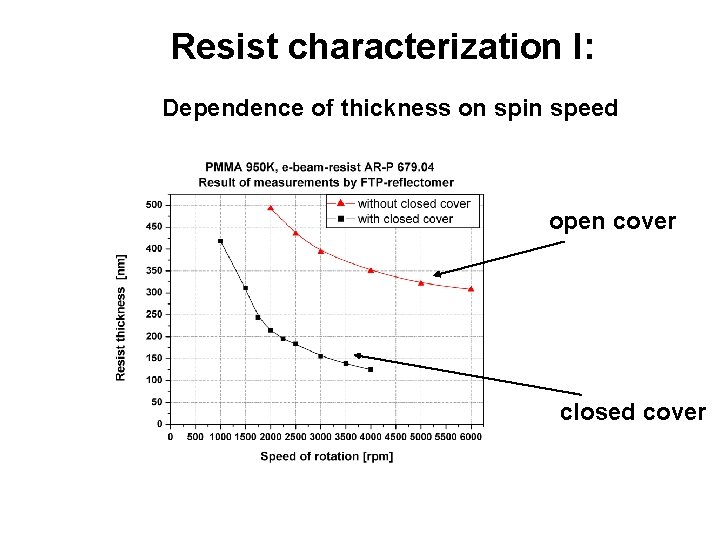
Resist characterization I: Dependence of thickness on spin speed open cover closed cover
Resist characterization II: Contrast curves
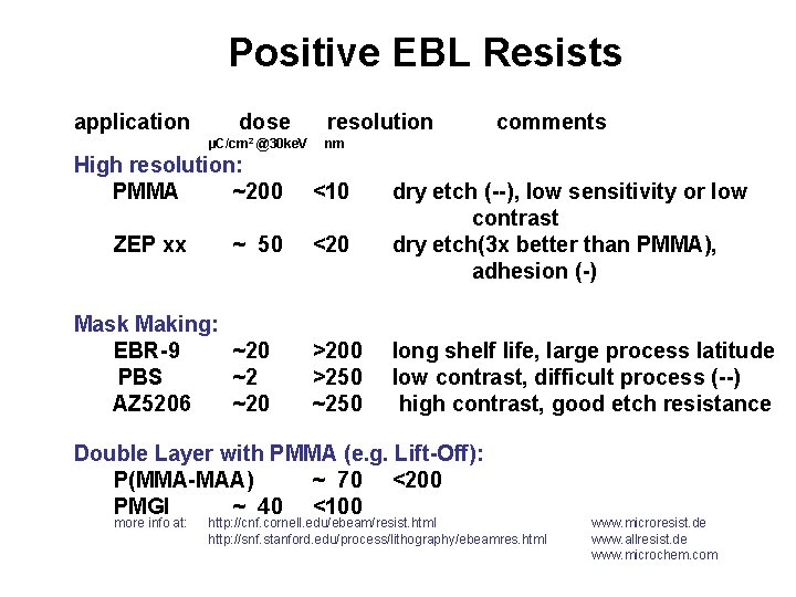
Positive EBL Resists application dose µC/cm 2 @30 ke. V High resolution: PMMA ~200 ZEP xx ~ 50 Mask Making: EBR-9 ~20 PBS ~2 AZ 5206 ~20 resolution nm <10 <20 >200 >250 ~250 dry etch (--), low sensitivity or low contrast dry etch(3 x better than PMMA), adhesion (-) long shelf life, large process latitude low contrast, difficult process (--) high contrast, good etch resistance Double Layer with PMMA (e. g. Lift-Off): P(MMA-MAA) ~ 70 <200 PMGI ~ 40 <100 more info at: comments http: //cnf. cornell. edu/ebeam/resist. html http: //snf. stanford. edu/process/lithography/ebeamres. html www. microresist. de www. allresist. de www. microchem. com
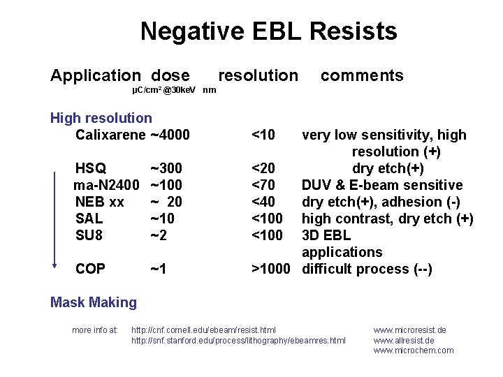
Negative EBL Resists Application dose resolution comments µC/cm 2 @30 ke. V nm High resolution Calixarene ~4000 HSQ ma-N 2400 NEB xx SAL SU 8 ~300 ~100 ~ 20 ~10 ~2 COP ~1 <10 very low sensitivity, high resolution (+) <20 dry etch(+) <70 DUV & E-beam sensitive <40 dry etch(+), adhesion (-) <100 high contrast, dry etch (+) <100 3 D EBL applications >1000 difficult process (--) Mask Making more info at: http: //cnf. cornell. edu/ebeam/resist. html http: //snf. stanford. edu/process/lithography/ebeamres. html www. microresist. de www. allresist. de www. microchem. com
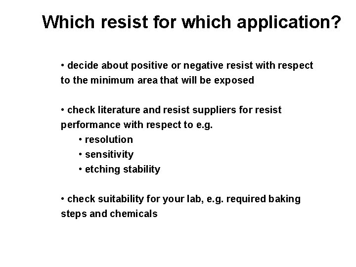
Which resist for which application? • decide about positive or negative resist with respect to the minimum area that will be exposed • check literature and resist suppliers for resist performance with respect to e. g. • resolution • sensitivity • etching stability • check suitability for your lab, e. g. required baking steps and chemicals
EBL Applications
PMMA 950 K for High Resolution • resist thickness: 45 nm • closed cover • developing 15 s without moving sample linewidth < 20 nm reproducibel! HEMT 16 nm line width 100 nm gate 50 nm lines
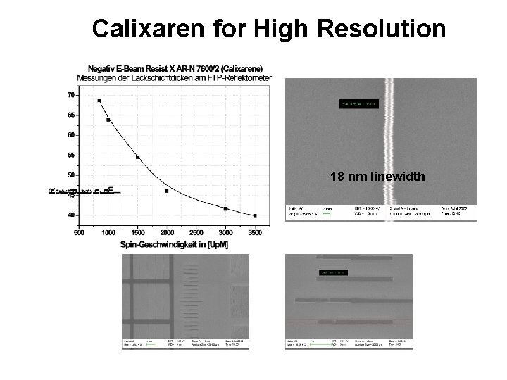
Calixaren for High Resolution 18 nm linewidth
Resists - 3 Dimensional Lithography Gradation Curve Contrast Conventional lithography Third Dimension! Positive resist Conventional Negative resist lithography
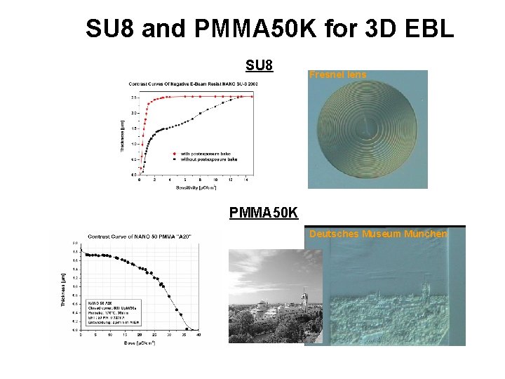
SU 8 and PMMA 50 K for 3 D EBL SU 8 Fresnel lens PMMA 50 K Deutsches Museum München
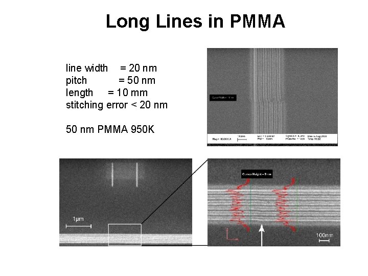
Long Lines in PMMA line width = 20 nm pitch = 50 nm length = 10 mm stitching error < 20 nm 50 nm PMMA 950 K
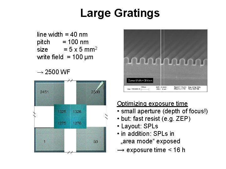
Large Gratings line width = 40 nm pitch = 100 nm size = 5 x 5 mm 2 write field = 100 µm → 2500 WF Optimizing exposure time • small aperture (depth of focus!) • but: fast resist (e. g. ZEP) • Layout: SPLs • in addition: SPLs in „area mode“ exposed → exposure time < 16 h
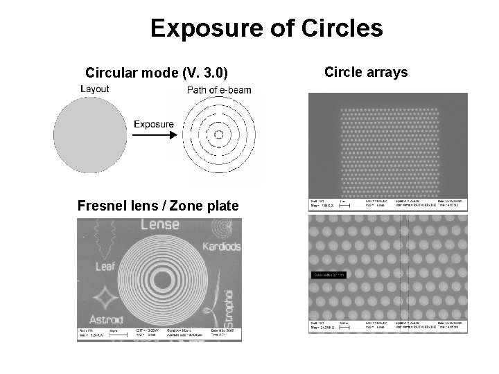
Exposure of Circles Circular mode (V. 3. 0) Fresnel lens / Zone plate Circle arrays
Proximity Effect Each pattern element needs a different dose - here shown by colors -
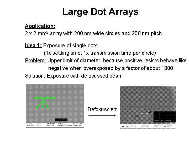
Large Dot Arrays Application: 2 x 2 mm 2 array with 200 nm wide circles and 250 nm pitch Idea 1: Exposure of single dots (1 x settling time, 1 x transmission time per circle) Problem: Upper limit of diameter, because positive resists behave like negative when overexposed by a factor of about 1000 Solution: Exposure with defocussed beam resist residues Defokussiert
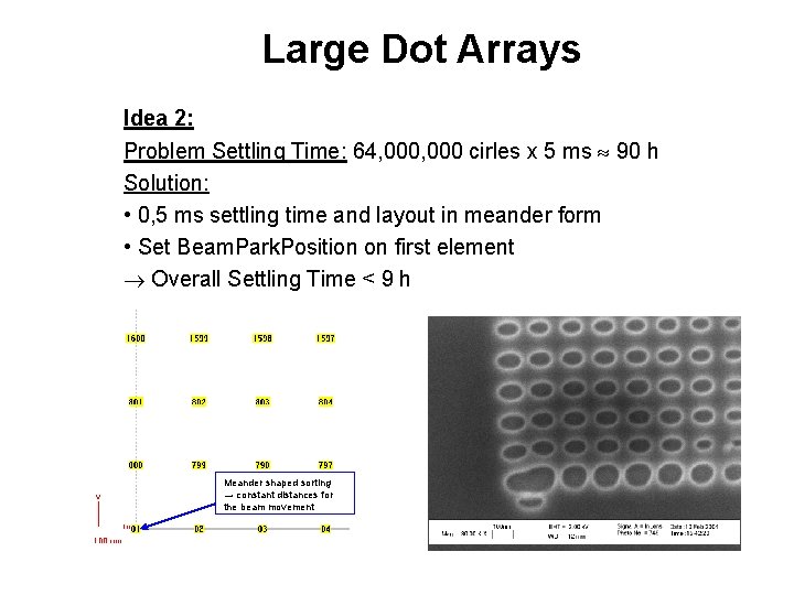
Large Dot Arrays Idea 2: Problem Settling Time: 64, 000 cirles x 5 ms 90 h Solution: • 0, 5 ms settling time and layout in meander form • Set Beam. Park. Position on first element Overall Settling Time < 9 h Meander shaped sorting → constant distances for the beam movement