Lithography and etching 2019 sami franssilaaalto fi Chapters

- Slides: 41

Lithography and etching 2019 sami. franssila@aalto. fi Chapters 9, 11

Outline • lithography = photoresist pattern formation • etching = transfer of photoresist pattern into solid material • stripping = removal of photoresist after etching the pattern • isotropic (wet) etching • anisotropic (plasma) etching

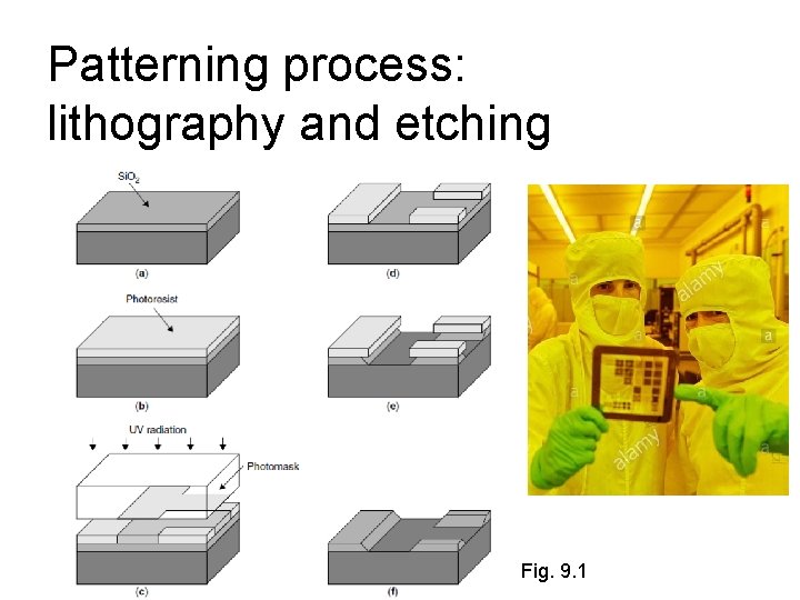
Patterning process: lithography and etching Fig. 9. 1

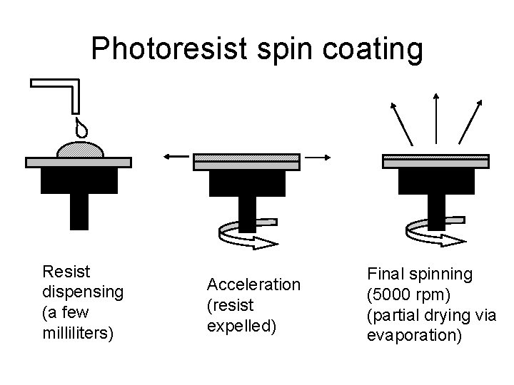
Photoresist spin coating Resist dispensing (a few milliliters) Acceleration (resist expelled) Final spinning (5000 rpm) (partial drying via evaporation)

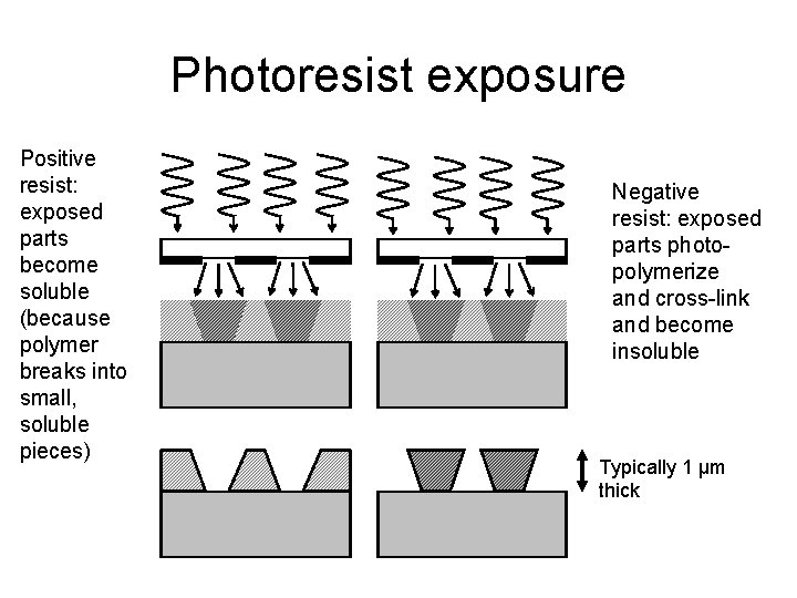
Photoresist exposure Positive resist: exposed parts become soluble (because polymer breaks into small, soluble pieces) Negative resist: exposed parts photopolymerize and cross-link and become insoluble Typically 1 µm thick

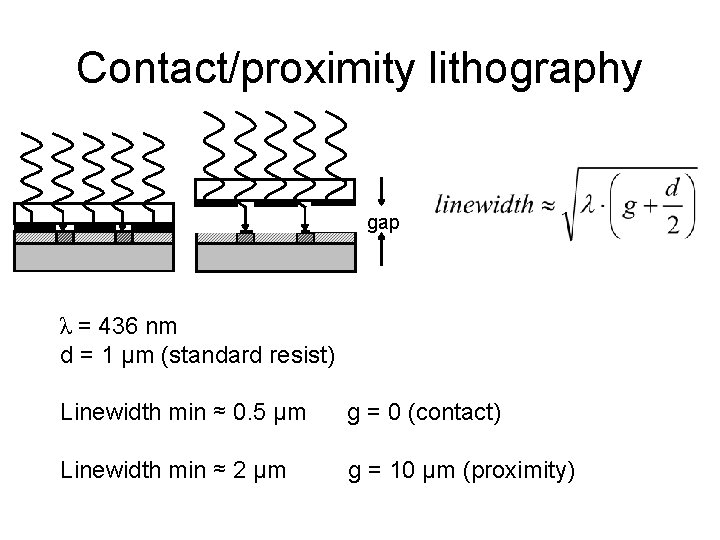
Contact/proximity lithography gap λ = 436 nm d = 1 µm (standard resist) Linewidth min ≈ 0. 5 µm g = 0 (contact) Linewidth min ≈ 2 µm g = 10 µm (proximity)

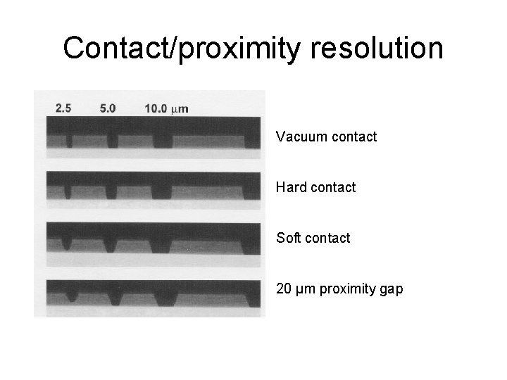
Contact/proximity resolution Vacuum contact Hard contact Soft contact 20 µm proximity gap

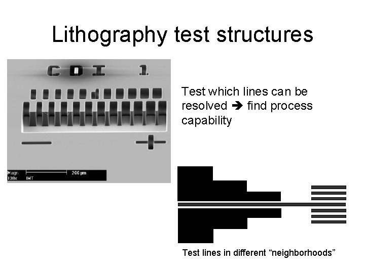
Lithography test structures Test which lines can be resolved find process capability Test lines in different “neighborhoods”

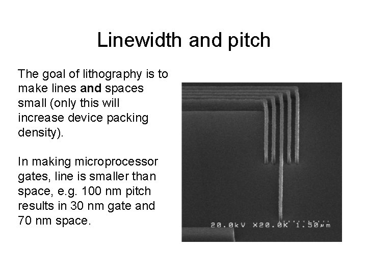
Linewidth and pitch The goal of lithography is to make lines and spaces small (only this will increase device packing density). In making microprocessor gates, line is smaller than space, e. g. 100 nm pitch results in 30 nm gate and 70 nm space.

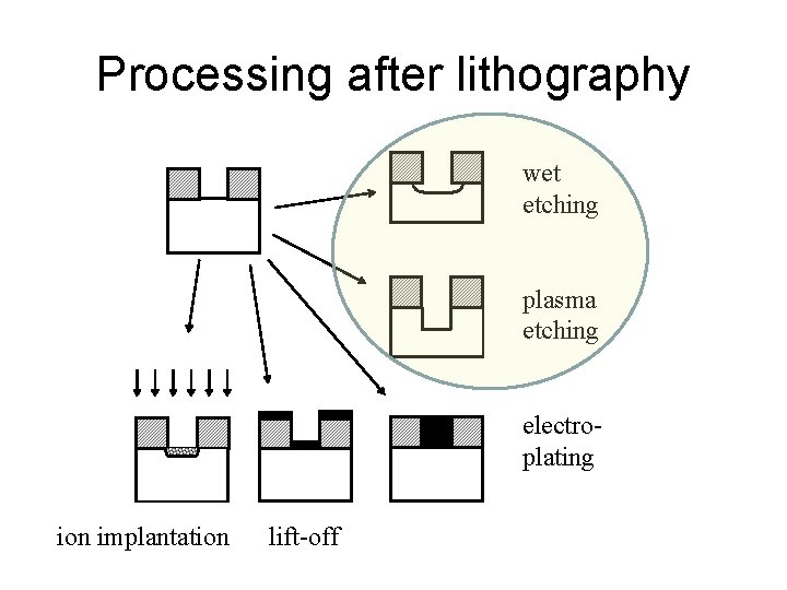
Processing after lithography wet etching plasma etching electroplating ion implantation lift-off

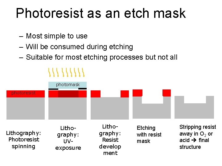
Photoresist as an etch mask – Most simple to use – Will be consumed during etching – Suitable for most etching processes but not all photomask photoresist Lithography: Photoresist spinning Lithography: UVexposure Lithography: Resist develop ment Etching with resist mask Stripping resist away in O 2 or acid final structure

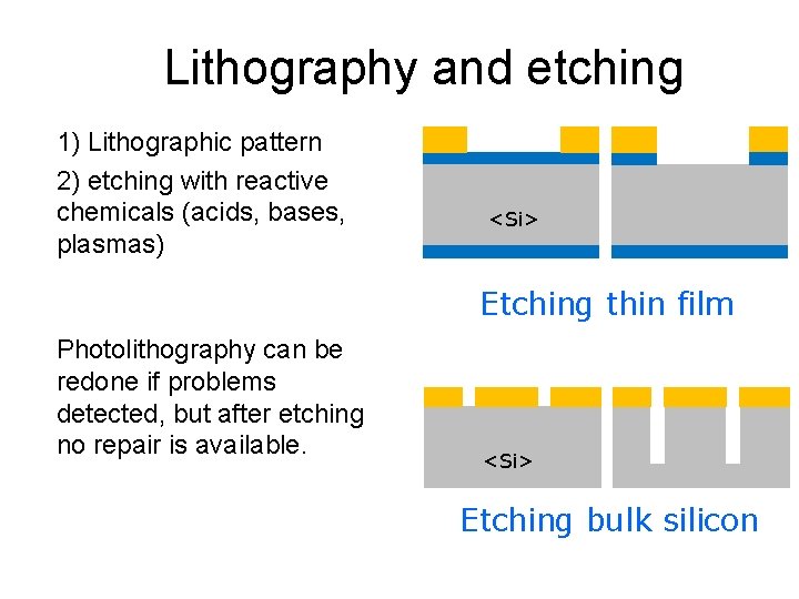
Lithography and etching 1) Lithographic pattern 2) etching with reactive chemicals (acids, bases, plasmas) <Si> Etching thin film Photolithography can be redone if problems detected, but after etching no repair is available. <Si> Etching bulk silicon

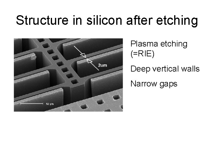
Structure in silicon after etching Plasma etching (=RIE) Deep vertical walls Narrow gaps

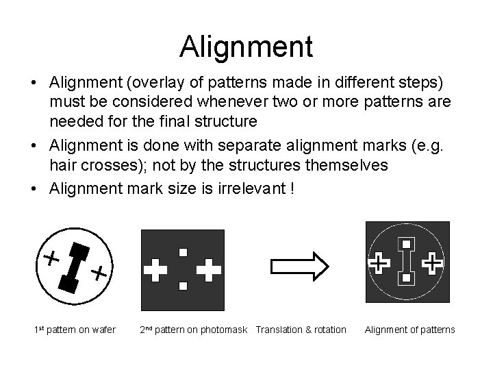
Alignment • Alignment (overlay of patterns made in different steps) must be considered whenever two or more patterns are needed for the final structure • Alignment is done with separate alignment marks (e. g. hair crosses); not by the structures themselves • Alignment mark size is irrelevant ! 1 st pattern on wafer 2 nd pattern on photomask Translation & rotation Alignment of patterns

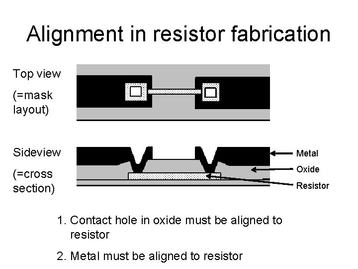
Alignment in resistor fabrication Top view (=mask layout) Sideview Metal (=cross section) Oxide Resistor 1. Contact hole in oxide must be aligned to resistor 2. Metal must be aligned to resistor

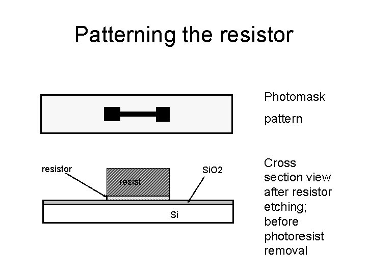
Patterning the resistor Photomask pattern resistor Si. O 2 resist Si Cross section view after resistor etching; before photoresist removal

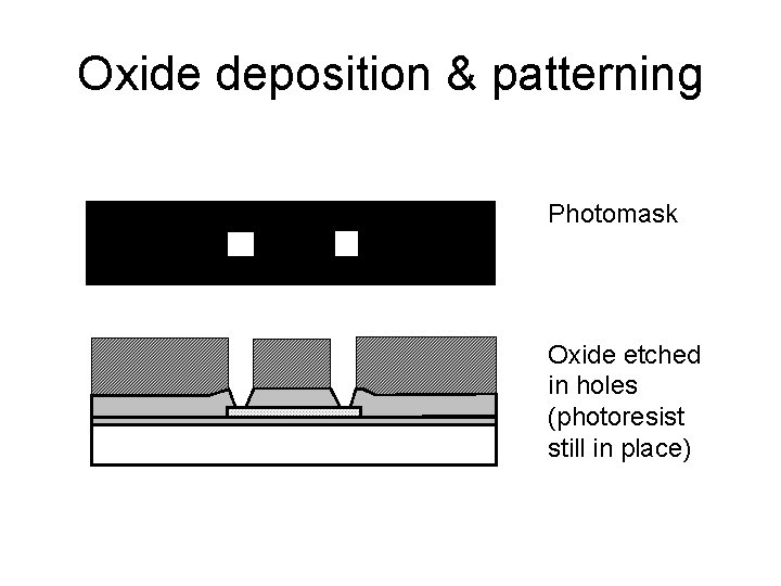
Oxide deposition & patterning Photomask Oxide etched in holes (photoresist still in place)

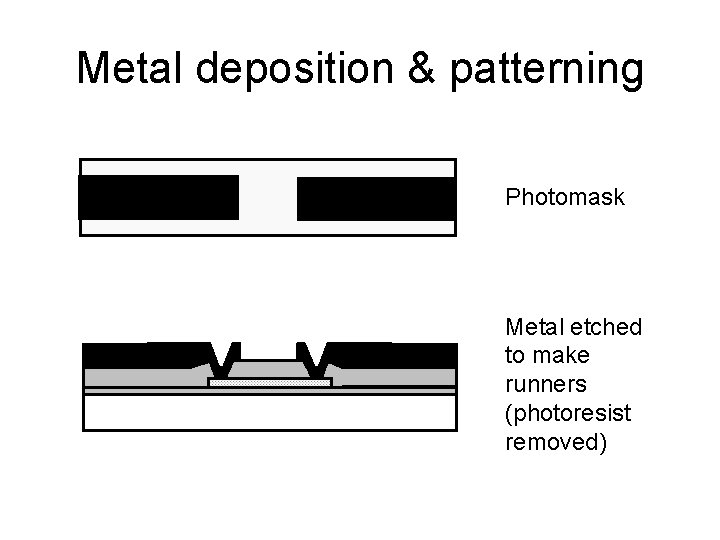
Metal deposition & patterning Photomask Metal etched to make runners (photoresist removed)

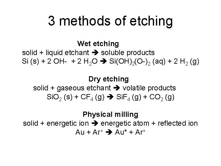
3 methods of etching Wet etching solid + liquid etchant soluble products Si (s) + 2 OH- + 2 H 2 O Si(OH)2(O-)2 (aq) + 2 H 2 (g) Dry etching solid + gaseous etchant volatile products Si. O 2 (s) + CF 4 (g) Si. F 4 (g) + CO 2 (g) Physical milling solid + energetic ion energetic atom + reflected ion Au + Ar+ Au* + Ar+

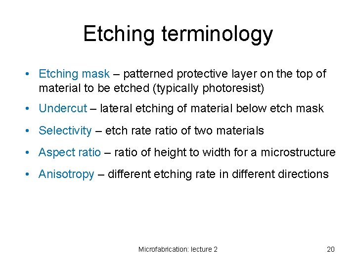
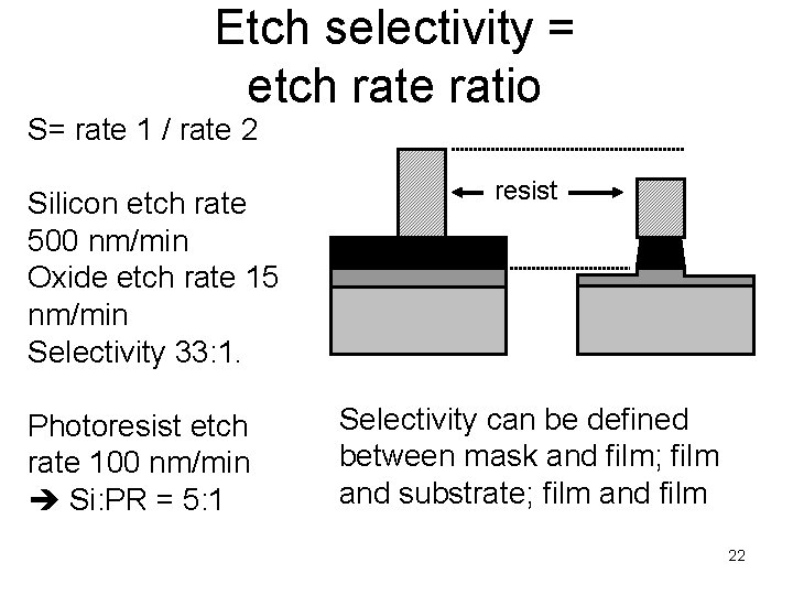
Etching terminology • Etching mask – patterned protective layer on the top of material to be etched (typically photoresist) • Undercut – lateral etching of material below etch mask • Selectivity – etch rate ratio of two materials • Aspect ratio – ratio of height to width for a microstructure • Anisotropy – different etching rate in different directions Microfabrication: lecture 2 20

Quizz • What is a photomask ? • How does it relate to etch mask ? 21

Etch selectivity = etch rate ratio S= rate 1 / rate 2 Silicon etch rate 500 nm/min Oxide etch rate 15 nm/min Selectivity 33: 1. Photoresist etch rate 100 nm/min Si: PR = 5: 1 resist Selectivity can be defined between mask and film; film and substrate; film and film 22

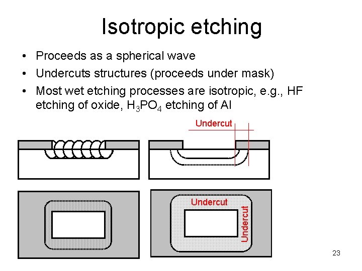
Isotropic etching • Proceeds as a spherical wave • Undercuts structures (proceeds under mask) • Most wet etching processes are isotropic, e. g. , HF etching of oxide, H 3 PO 4 etching of Al Undercut 23

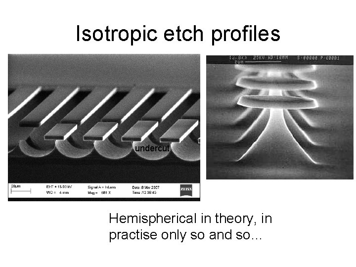
Isotropic etch profiles undercut Hemispherical in theory, in practise only so and so…

Wet etching • • • Usually isotropic (Near) perfect selectivity Each material needs different chemistry Surface finish smooth High throughput because batch process Cheap equipment • Not suitable for narrow lines and spaces !!! 25

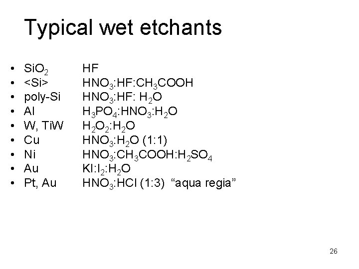
Typical wet etchants • • • Si. O 2 <Si> poly-Si Al W, Ti. W Cu Ni Au Pt, Au HF HNO 3: HF: CH 3 COOH HNO 3: HF: H 2 O H 3 PO 4: HNO 3: H 2 O 2: H 2 O HNO 3: H 2 O (1: 1) HNO 3: CH 3 COOH: H 2 SO 4 KI: I 2: H 2 O HNO 3: HCl (1: 3) “aqua regia” 26

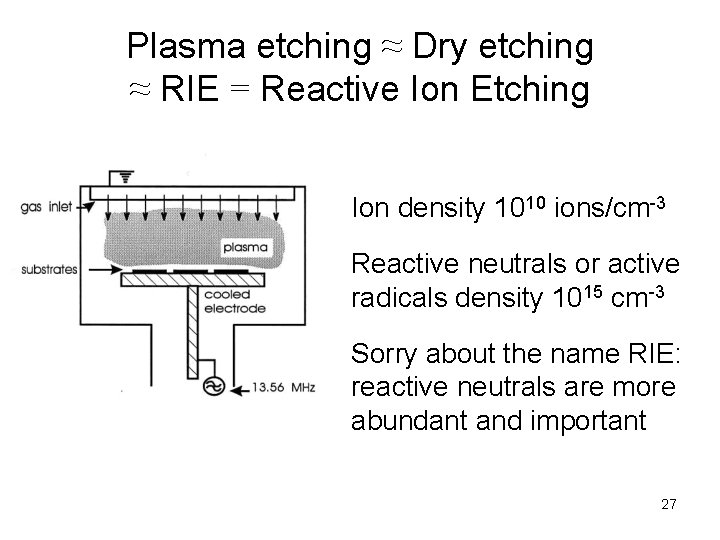
Plasma etching ≈ Dry etching ≈ RIE = Reactive Ion Etching Ion density 1010 ions/cm-3 Reactive neutrals or active radicals density 1015 cm-3 Sorry about the name RIE: reactive neutrals are more abundant and important 27

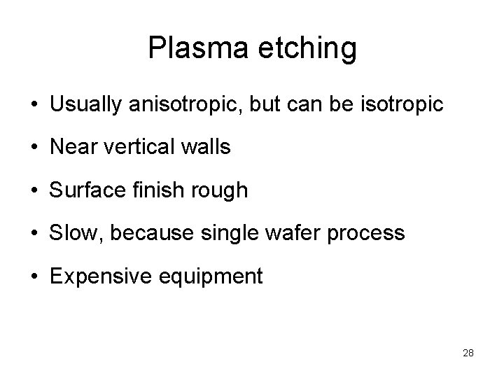
Plasma etching • Usually anisotropic, but can be isotropic • Near vertical walls • Surface finish rough • Slow, because single wafer process • Expensive equipment 28

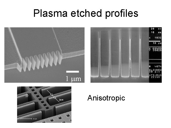
Plasma etched profiles Anisotropic

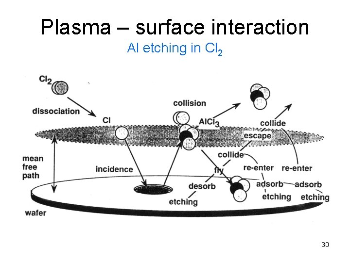
Plasma – surface interaction Al etching in Cl 2 30

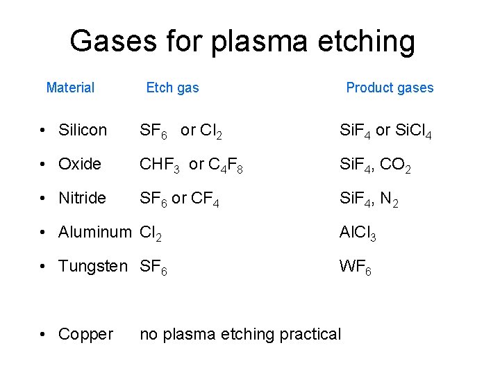
Gases for plasma etching Material Etch gas Product gases • Silicon SF 6 or Cl 2 Si. F 4 or Si. Cl 4 • Oxide CHF 3 or C 4 F 8 Si. F 4, CO 2 • Nitride SF 6 or CF 4 Si. F 4, N 2 • Aluminum Cl 2 Al. Cl 3 • Tungsten SF 6 WF 6 • Copper no plasma etching practical

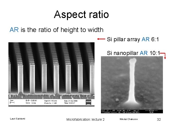
Aspect ratio AR is the ratio of height to width Si pillar array AR 6: 1 Si nanopillar AR 10: 1 Lauri Sainiemi Microfabrication: lecture 2 Nikolai Chekurov 32

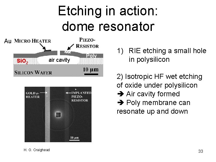
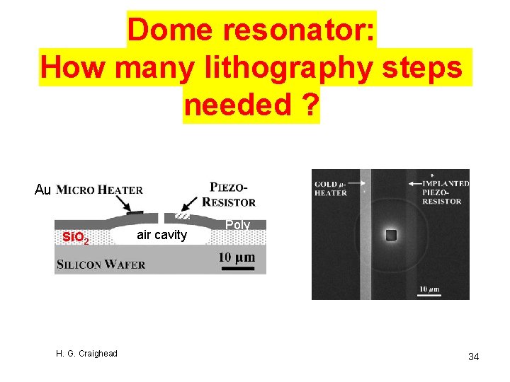
Etching in action: dome resonator Au Si. O 2 air cavity Poly 1) RIE etching a small hole in polysilicon 2) Isotropic HF wet etching of oxide under polysilicon Air cavity formed Poly membrane can resonate up and down H. G. Craighead 33

Dome resonator: How many lithography steps needed ? Au Si. O 2 H. G. Craighead air cavity Poly 34

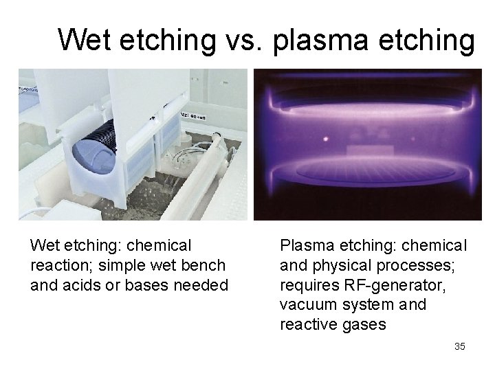
Wet etching vs. plasma etching Wet etching: chemical reaction; simple wet bench and acids or bases needed Plasma etching: chemical and physical processes; requires RF-generator, vacuum system and reactive gases 35

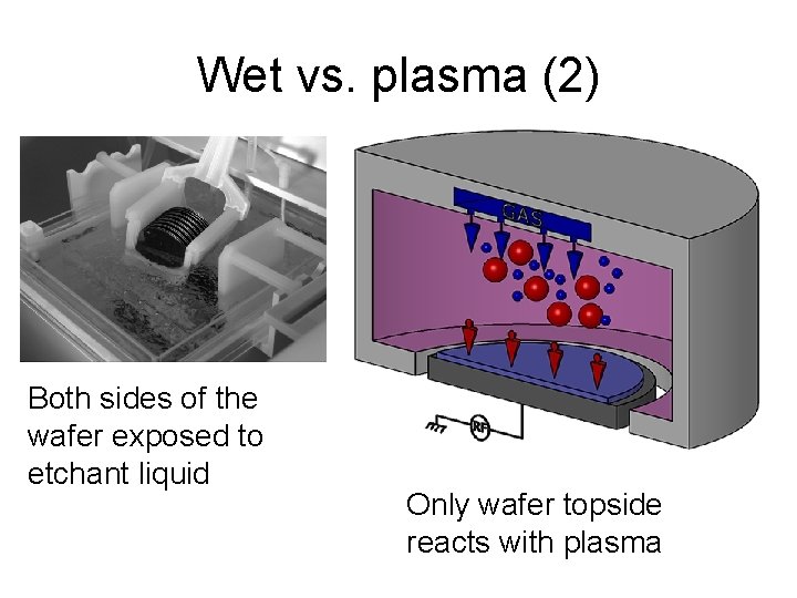
Wet vs. plasma (2) Both sides of the wafer exposed to etchant liquid Only wafer topside reacts with plasma

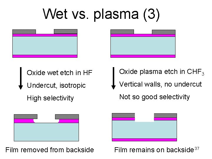
Wet vs. plasma (3) Oxide wet etch in HF Oxide plasma etch in CHF 3 Undercut, isotropic Vertical walls, no undercut High selectivity Not so good selectivity Film removed from backside Film remains on backside 37

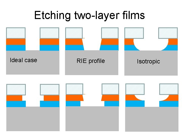
Etching two-layer films Ideal case RIE profile Isotropic

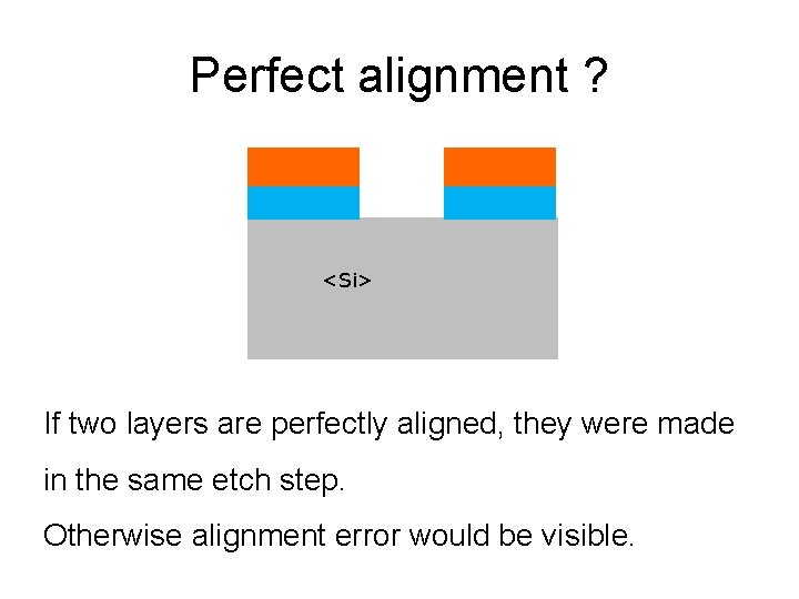
Perfect alignment ? <Si> If two layers are perfectly aligned, they were made in the same etch step. Otherwise alignment error would be visible.

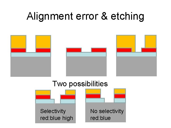
Alignment error & etching Two possibilities Selectivity red: blue high No selectivity red: blue

Lithographic patterning Photoresist is UV-exposed It serves as an interim mask Etching produces permanent pattern in metal/silicon/oxide Photoresist is stripped in the end Smaller linewidth require more expensive lithography Large linewidths can be wet etched Small linewidths require plasma etching