Lithographic Processes q Pattern generation and transfer Circuit
- Slides: 16

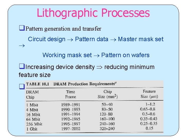
Lithographic Processes q. Pattern generation and transfer Circuit design Pattern data Master mask set Working mask set Pattern on wafers q. Increasing device density reducing minimum feature size q Through-put consideration

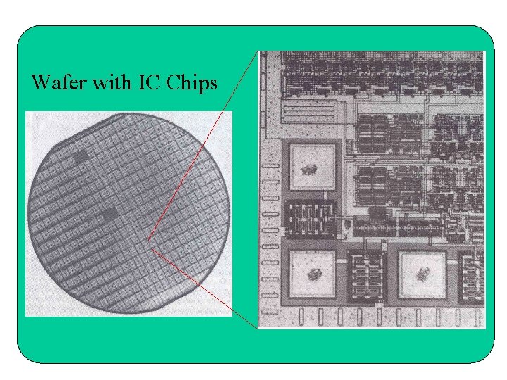
Wafer with IC Chips

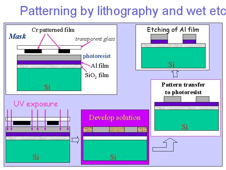
Patterning by lithography and wet etc Mask Etching of Al film Cr patterned film transparent glass photoresist Si Al film Si. O 2 film Pattern transfer to photoresist Si UV exposure Develop solution Si Si Si

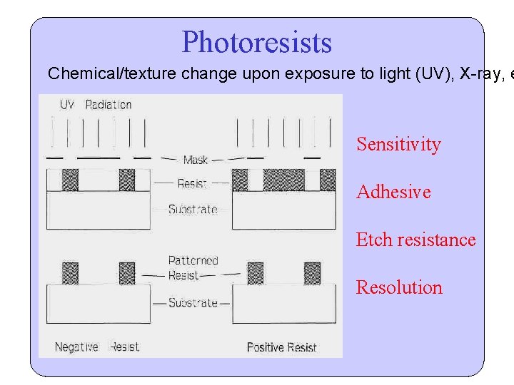
Photoresists Chemical/texture change upon exposure to light (UV), X-ray, e Sensitivity Adhesive Etch resistance Resolution

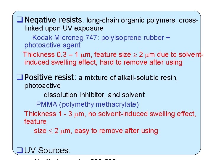
q Negative resists: long-chain organic polymers, cross- linked upon UV exposure Kodak Microneg 747: polyisoprene rubber + photoactive agent Thickness 0. 3 – 1 m, feature size 2 m due to solventinduced swelling effect, hard to remove after using q Positive resist: a mixture of alkali-soluble resin, photoactive dissolution inhibitor, and solvent PMMA (polymethylmethacrylate) Thickness 1 - 3 m, no solvent-induced swelling effect, feature size 2 m, easy to remove after using q UV Sources:

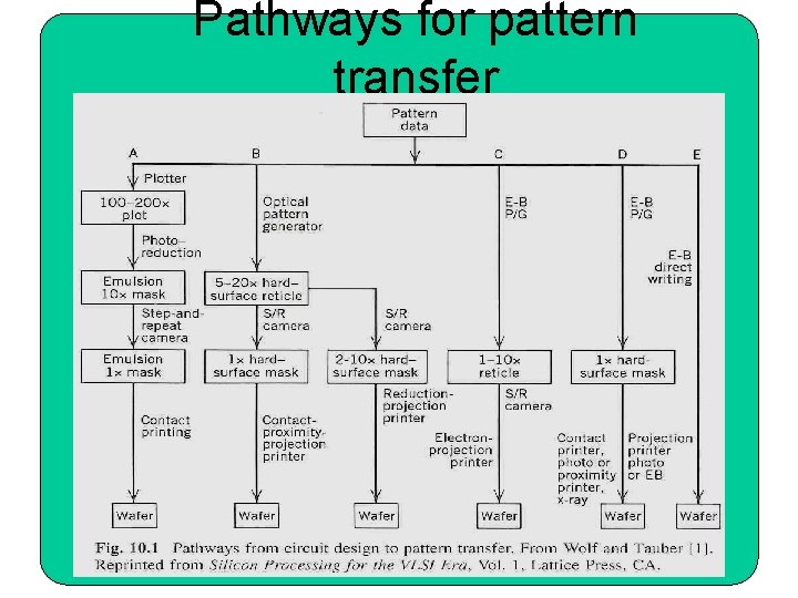
Pathways for pattern transfer

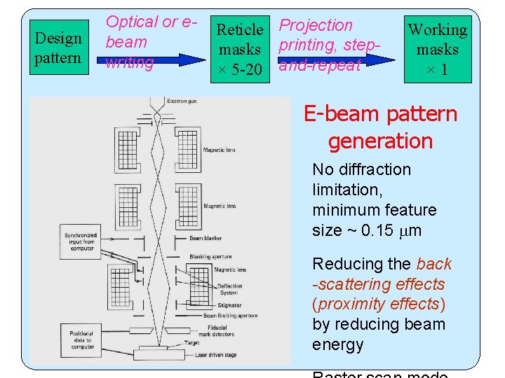
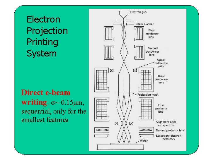
Design pattern Optical or ebeam writing Reticle Projection masks printing, step× 5 -20 and-repeat Working masks × 1 E-beam pattern generation No diffraction limitation, minimum feature size ~ 0. 15 m Reducing the back -scattering effects (proximity effects) by reducing beam energy

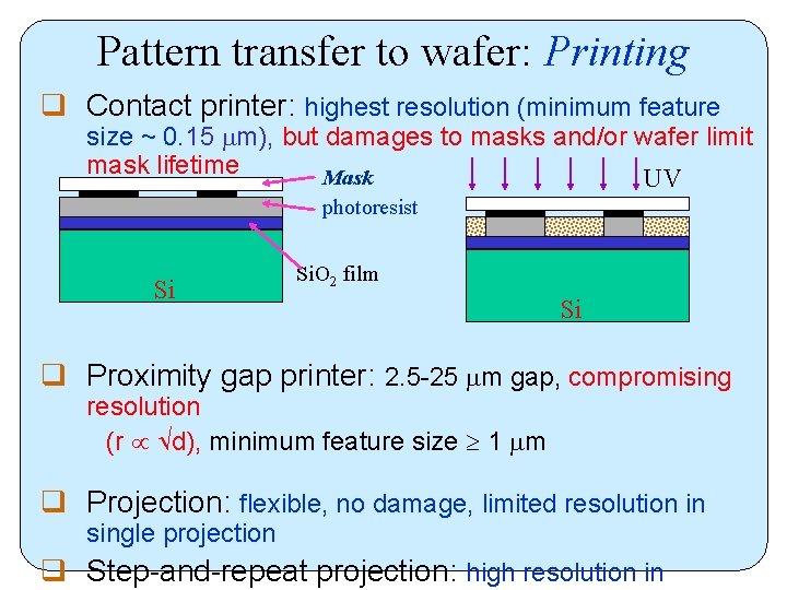
Pattern transfer to wafer: Printing q Contact printer: highest resolution (minimum feature size ~ 0. 15 m), but damages to masks and/or wafer limit mask lifetime Mask UV photoresist Si Si. O 2 film Si q Proximity gap printer: 2. 5 -25 m gap, compromising resolution (r d), minimum feature size 1 m q Projection: flexible, no damage, limited resolution in single projection q Step-and-repeat projection: high resolution in

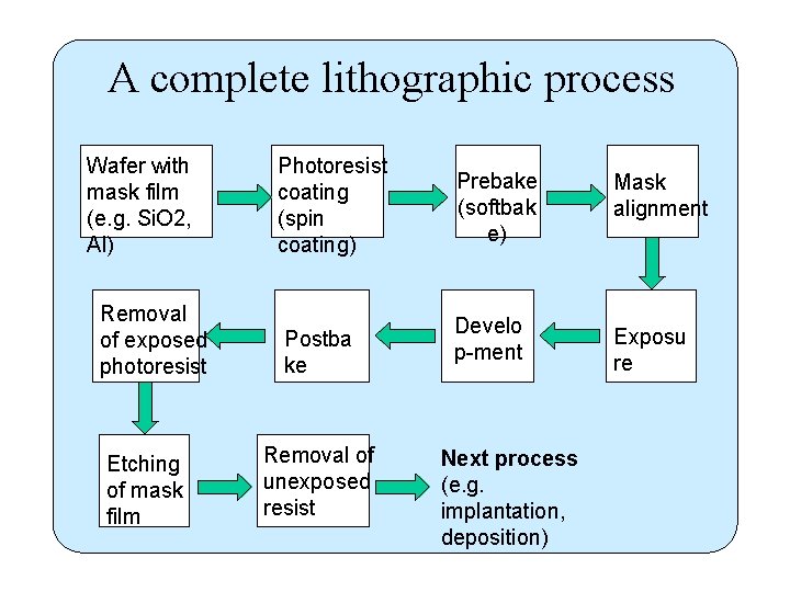
A complete lithographic process Wafer with mask film (e. g. Si. O 2, Al) Removal of exposed photoresist Etching of mask film Photoresist coating (spin coating) Postba ke Removal of unexposed resist Prebake (softbak e) Develo p-ment Next process (e. g. implantation, deposition) Mask alignment Exposu re

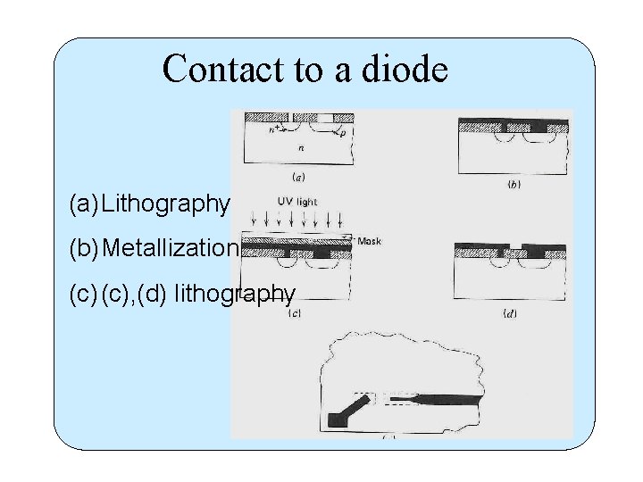
Contact to a diode (a) Lithography (b) Metallization (c), (d) lithography

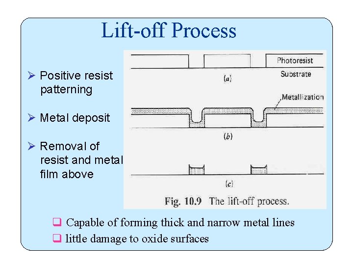
Lift-off Process Ø Positive resist patterning Ø Metal deposit Ø Removal of resist and metal film above q Capable of forming thick and narrow metal lines q little damage to oxide surfaces

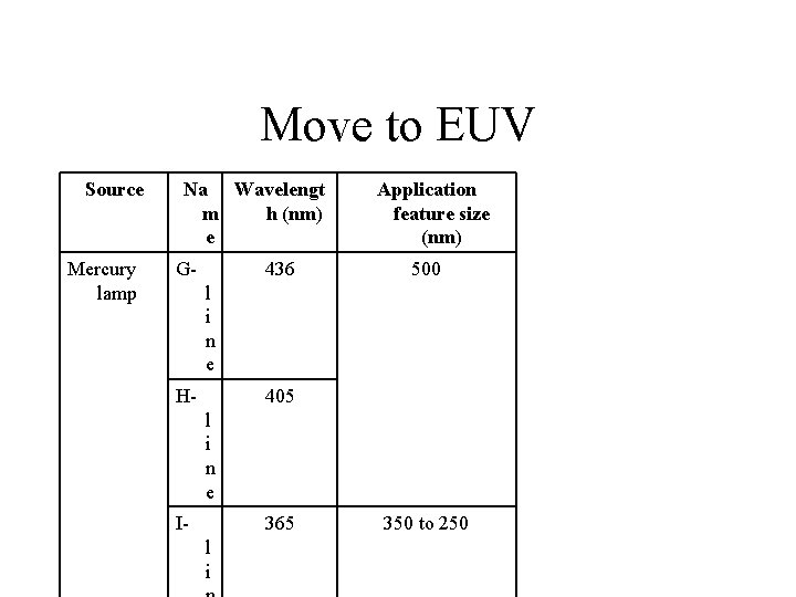
Move to EUV Source Mercury lamp Na Wavelengt m h (nm) e G- 436 Application feature size (nm) 500 l i n e H- 405 l i n e I- 365 l i 350 to 250

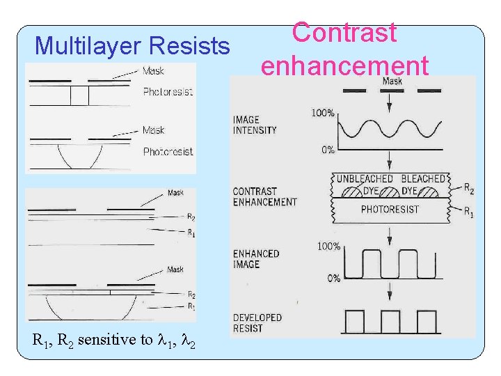
Multilayer Resists R 1, R 2 sensitive to 1, 2 Contrast enhancement

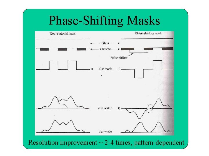
Phase-Shifting Masks Resolution improvement ~ 2 -4 times, pattern-dependent

Electron Projection Printing System Direct e-beam writing: ~ 0. 15 m, sequential, only for the smallest features

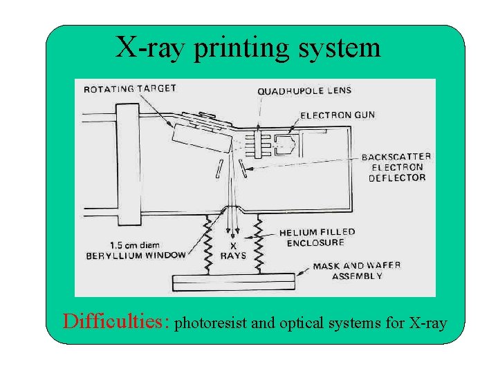
X-ray printing system Difficulties: photoresist and optical systems for X-ray