Lithographic processes Lithographic processes o Microcircuit fabrication has

Lithographic processes

Lithographic processes o Microcircuit fabrication has various doping patterns on Si wafer and interconnects. o These operations are carried by lithographic processes at various points in fabrication o Typically 5 -20 operations are required on each wafer. o Thus lithographic processes play an important role in microcircuit technology
 Generation of a reticle mask-")
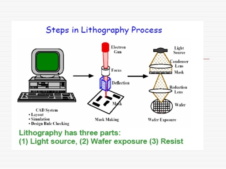
Lithographic processes o The process has two parts: 1) Generation of a reticle mask- ckt layout 2) Transfer of pattern on to Si waferplacement of mask o The methods used are: 1)Optical lithography 2)Electron beam lithography 3)X-ray lithography 4)Ion Beam. Techniques

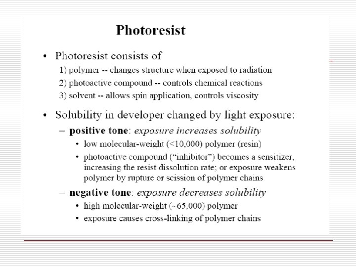
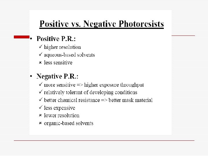
Photoreactive Materials o Two types of photoresist processes o o Positive photoresist: image same as object. Material becomes soluble after exposure to radiation Negative photoresist: image opposite as object. Material hardens on exposure to radiation

Properties of photoresist o o o Sensistivity Adhesion Etch resistance Stability Uniformity Contaminants and particles

Photoresist

Pattern Generation o Pattern generation : layout pattern is put onto a reticle or master mask o E-beam and optical techniques are used o Working masks are made from master mask by contact printing to define pattern on each wafer to be processed

Pattern Generation o Optical and e-beam technique: optical: diffraction limit is set by wavelength of light. e-beam: no such limit. But suffer back scatter leading to proximity effects. Controlled by reducing beam energy. Presently e-beam is used for pattern generation for a min feature size of 0. 15μm
 Magnetic lens 2) Beam blanker 3) Computer controlled")
E-beam pattern generation system Components: 1) Magnetic lens 2) Beam blanker 3) Computer controlled Deflection system 4) Fiducial mark detectors Scan : 1) Raster scan: rectangular strips of circuit are scanned 1) Vector scan: scans only the feature Writing time set by intensity of beam. typical 4 h for 20 cm by 20 cm mask size
 Clear with small opaque")
Image Reversal o Mask can be of two types 1) Clear with small opaque regions 2) Dark with small transparent regions Issue: light scattering due to dust and defects Positive photoresist with negative image-Image reversal

Pattern Transfer
 highest resolution 2)mask damage 3) short life o Proximity")
Comparison o Contact Printing: 1) highest resolution 2)mask damage 3) short life o Proximity printing: 1) gap of 2. 5 to 25μm. limits feature size o Projection printing: 1) flexible 2) no damage to the mask 3) images the complete wafer in one operation. Reduces resolution for large area

Optical printing

Pattern transfer

Pattern transfer

Pattern transfer

Pattern transfer

Steps in opening a window a d semiconductor b UV e c mask f positive photoresist Masking film

Issues in lithography o Mask defectsvisual defects, cleanliness o Pattern transfer defects -undercutting of resist -dimensional variations - dust particles - scratches and tear - step coverage
- Slides: 22