Linear Current Starved Delay Element ICEST 2005 Ni

- Slides: 17

Linear Current Starved Delay Element ICEST 2005, Niš Goran S. Jovanović and Mile K. Stojčev Faculty of Electronic Engineering, Niš, Serbia and Montenegro

Definitions of some standard terms Variable delay elements (VDEs)-definition VDEs are inverter–based circuits used for fine, precise, and accurate pulse delay control in a high-speed digital and mixed integrated circuits. How is achieved variable delay? Using delay line (DL). A chain of VDEs forms DL. Where we meet delay lines? DLs are constituents of: • • DLLs (Delay Locked Loops), TDCs (Time-to-Digital Converters), VCOs (Voltage Controlled Oscillators), PWCLs (Pulse-Width Control Loops), etc.

Typical Applications of DLs • DLs are used as constituent in DLLs in order to: – achieve correct synchronization between different digital blocks (CPU and SDRAM interface, . . . ), – eliminate clock skew and jitter within VLSI ICs. • Vernier delay patterns implemented as TDCs, usually composed with two DLs. • DLs connected in a ring are building blocks of VCO in PLLs. • DLs are constituents of Duty Cycle Correctors (DCCs) in systems with feedback loop.

Classification of delay line elements Variable delay line elements are classified as: • Digital Controlled Delay Elements (DCDEs) realized as series of delay elements of variable length (the number of elements in a chain determines the amount of the delay). • Voltage Controlled Delay Elements (VCDEs) efficient in applications where small, accurate, and precise amount of delay is necessary to achieve. VCDEs are realized using: q shunt capacitor, q current starved.

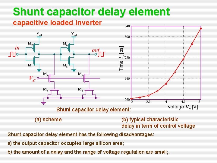
Shunt capacitor delay element capacitive loaded inverter Shunt capacitor delay element: (a) scheme (b) typical characteristic delay in term of control voltage Shunt capacitor delay element has the following disadvantages: a) the output capacitor occupies large silicon area; b) the amount of a delay and the range of voltage regulation are small; .

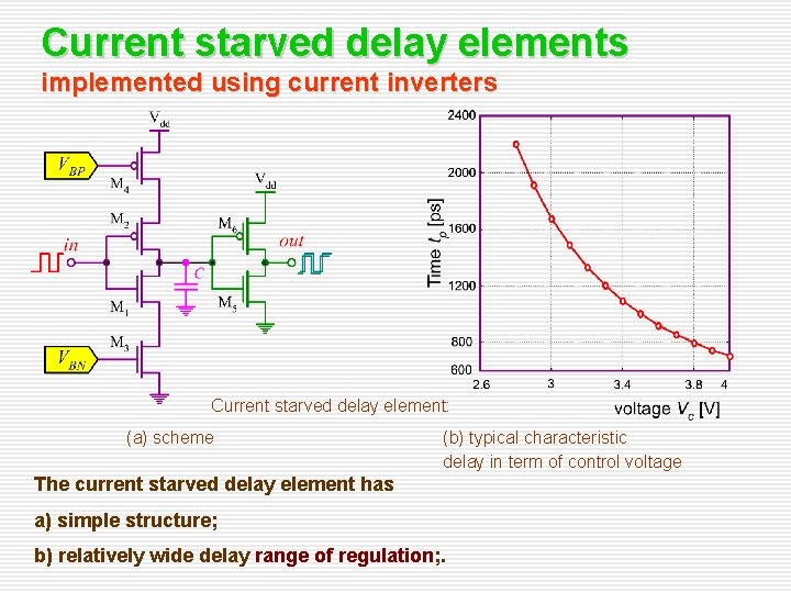
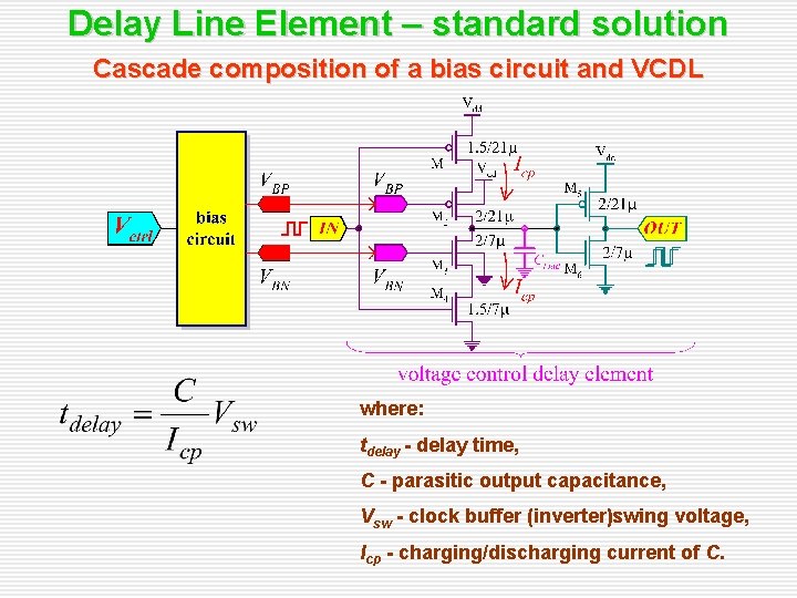
Current starved delay elements implemented using current inverters Current starved delay element: (a) scheme (b) typical characteristic delay in term of control voltage The current starved delay element has a) simple structure; b) relatively wide delay range of regulation; .

Common to both VCDLs Advantages: • Simple structures • Fine delay resolution Disadvantages: • Shunt Capacitor and Current Starved DLs have non linear transfer function, delay variation in term of control voltage Problem of VCDL realization was considered by: • • • Y. Moon, et al. , “An All Analog Multiphase Delay Locked Loop Using a Replica Delay Line for Wide Range Operation and Low Jitter Performance”, IEEE JSSC, vol. 35, No. 3, pp. 377 384, March 2000. M. Maymandi Nejad, M. Sachdev, “A digitally Programmable Delay Element: Design and Analysis”, IEEE Trans. on VLSI Systems, vol. 11, No. 5, October 2003. G. Jovanović, M. Stojčev, “Voltage Controlled Delay Line for Digital Signal”, Facta Universitatis, Series: Electronics and Energetic, vol. 16. No. 2, pp. 215 232, August 2003. . .

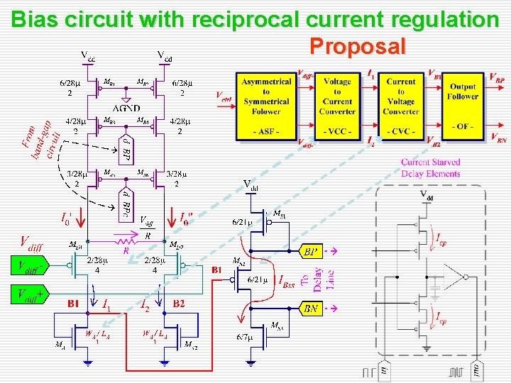
What we propose • • • Linearization of VCDL’s transfer function We use Current Starved DE. Why: – Simple structure – Relatively wide range of delay regulation • How we achieve linear VCDL? – We modify the bias circuit. – We use a non linear bias circuit which is based on the square law characteristics of a MOS transistor in saturation. – By a cascade connection of two non linear elements, the bias circuit and the current starved delay element, we obtain a linear transfer function (delay in terms of control voltage).

Delay Line Element – standard solution Cascade composition of a bias circuit and VCDL where: tdelay time, C parasitic output capacitance, Vsw clock buffer (inverter)swing voltage, Icp charging/discharging current of C.

Bias circuit with reciprocal current regulation Proposal

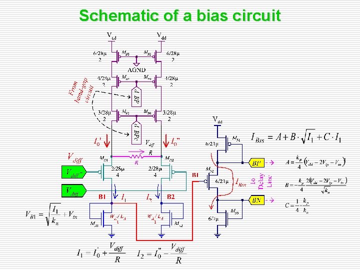
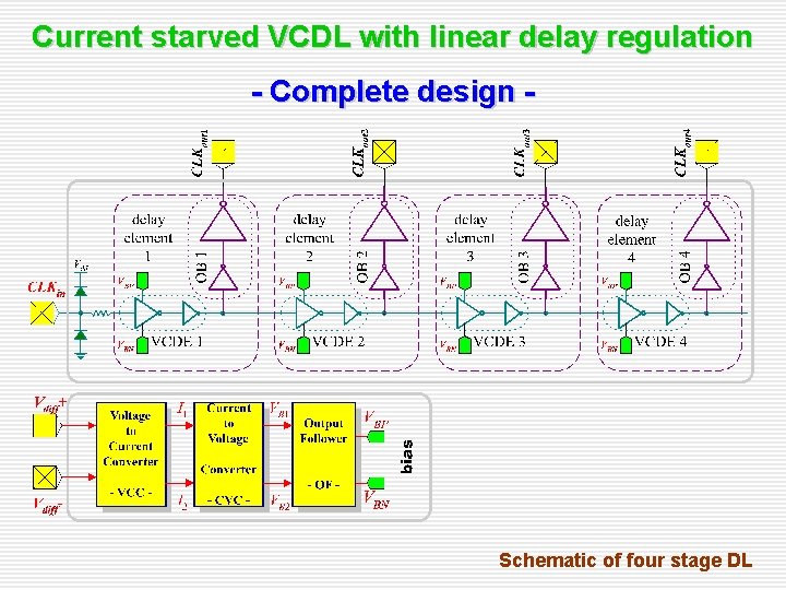
Schematic of a bias circuit

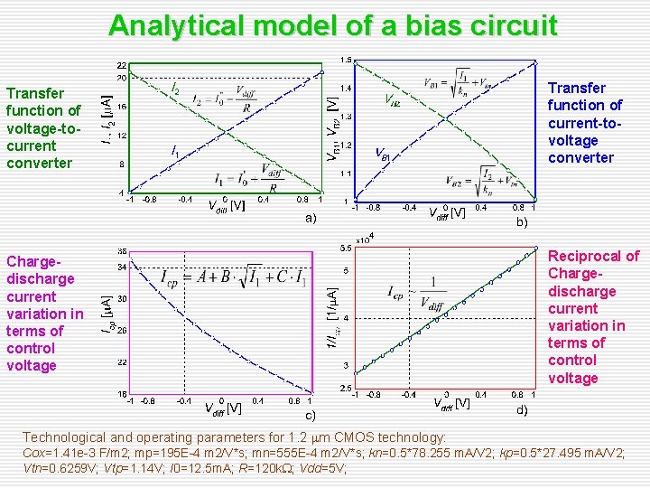
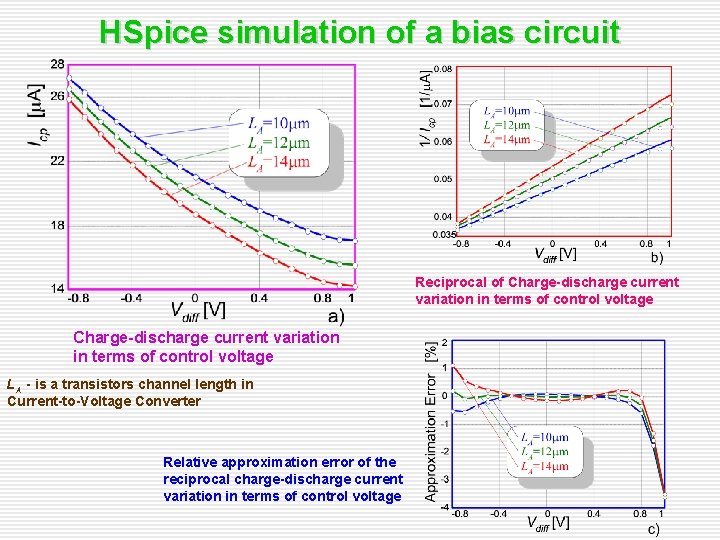
Analytical model of a bias circuit Transfer function of voltage to current converter Transfer function of current to voltage converter Charge discharge current variation in terms of control voltage Reciprocal of Charge discharge current variation in terms of control voltage Technological and operating parameters for 1. 2 mm CMOS technology: Cox=1. 41 e-3 F/m 2; mp=195 E-4 m 2/V*s; mn=555 E-4 m 2/V*s; kn=0. 5*78. 255 m. A/V 2; kp=0. 5*27. 495 m. A/V 2; Vtn=0. 6259 V; Vtp=1. 14 V; I 0=12. 5 m. A; R=120 k. W; Vdd=5 V;

HSpice simulation of a bias circuit Reciprocal of Charge discharge current variation in terms of control voltage LA is a transistors channel length in Current to Voltage Converter Relative approximation error of the reciprocal charge discharge current variation in terms of control voltage

Current starved VCDL with linear delay regulation Complete design Schematic of four stage DL

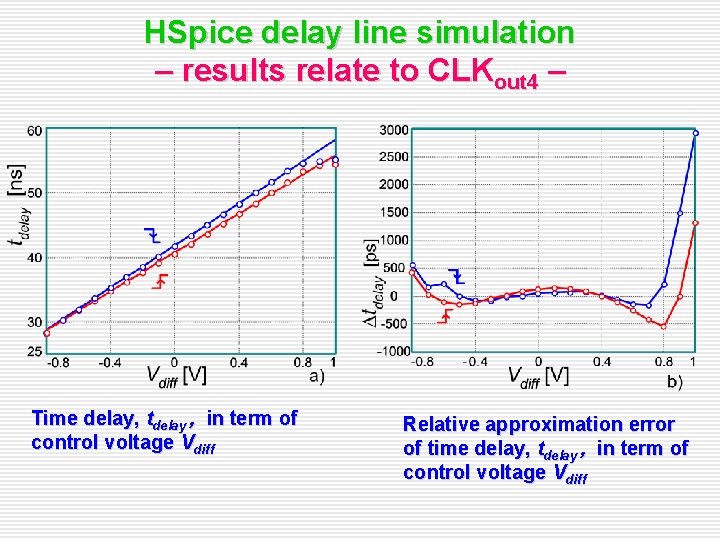
HSpice delay line simulation – results relate to CLKout 4 – Time delay, tdelay , in term of control voltage Vdiff Relative approximation error of time delay, tdelay , in term of control voltage Vdiff

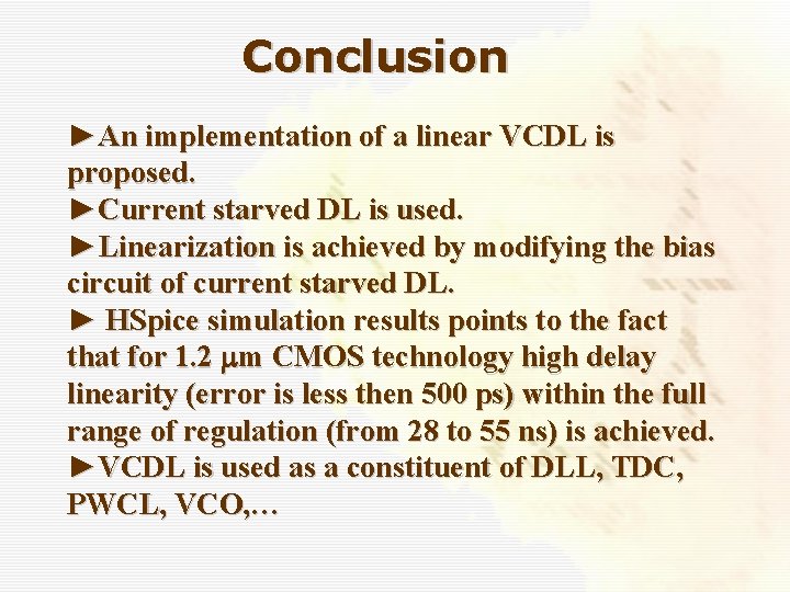
Conclusion ►An implementation of a linear VCDL is proposed. ►Current starved DL is used. ►Linearization is achieved by modifying the bias circuit of current starved DL. ► HSpice simulation results points to the fact that for 1. 2 mm CMOS technology high delay linearity (error is less then 500 ps) within the full range of regulation (from 28 to 55 ns) is achieved. ►VCDL is used as a constituent of DLL, TDC, PWCL, VCO, …

Q&A