Linear Analysis and Optimization of Stream Programs Andrew
- Slides: 48

Linear Analysis and Optimization of Stream Programs Andrew A. Lamb William Thies Saman Amarasinghe The New Laboratory for Computer Science and Artificial Intelligence Massachusetts Institute of Technology

Streaming Application Domain n n Based on audio, video, or data stream Increasingly prevalent and important n Embedded systems n n Desktop applications n n n Cell phones, handheld computers Streaming media Software radio • Real-time encryption • Graphics packages High-performance servers n n n Software routers (Example: Click) Cell phone base stations HDTV editing consoles The New Laboratory for Computer Science and Artificial Intelligence 2

Properties of Stream Programs n A large (possibly infinite) amount of data n n n Computation: apply multiple filters to data n n n Limited lifetime of each data item Little processing of each data item Each filter takes an input stream, does some processing, and produces an output stream Filters are independent and self-contained A regular, static computation pattern n n Filter graph is relatively constant A lot of opportunities for compiler optimizations The New Laboratory for Computer Science and Artificial Intelligence 3

The Stream. It Language n Goals: n n Provide a High-Level Programming Paradigm Improve Programmer Productivity Match Performance of Hand-Hacked Assembly Contributions n n Language Design, Structured Streams, Buffer Management (CC 2002) Exploiting Wire-Exposed Architectures (ASPLOS 2002) Scheduling of Static Dataflow Graphs (LCTES 2003) Domain Specific Optimizations (PLDI 2003) The New Laboratory for Computer Science and Artificial Intelligence 4

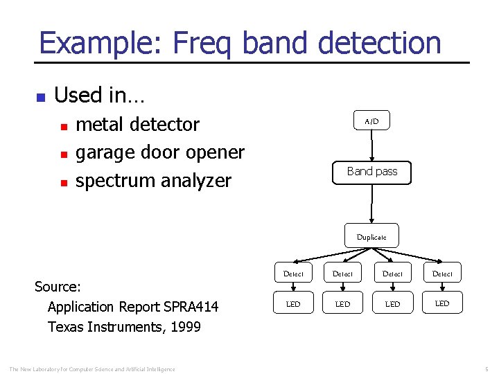
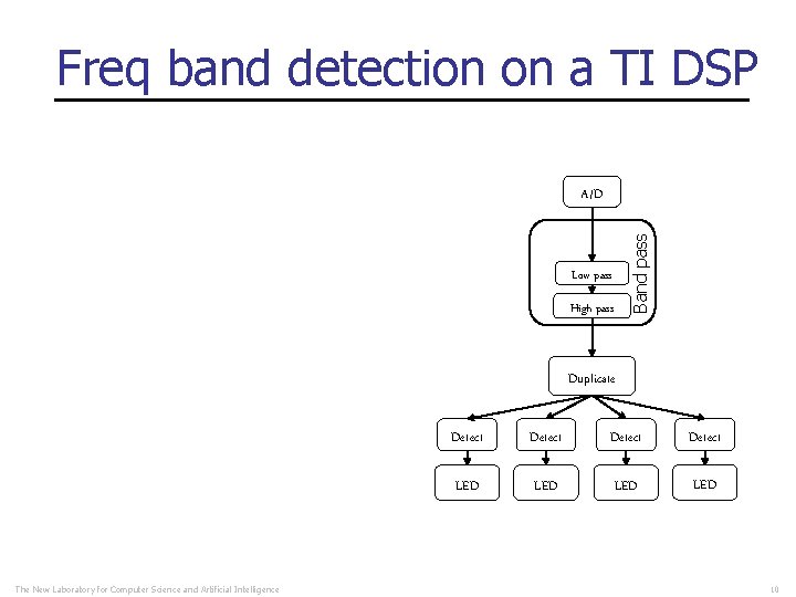
Example: Freq band detection n Used in… n n n metal detector garage door opener spectrum analyzer A/D Band pass Duplicate Source: Application Report SPRA 414 Texas Instruments, 1999 The New Laboratory for Computer Science and Artificial Intelligence Detect LED LED 5

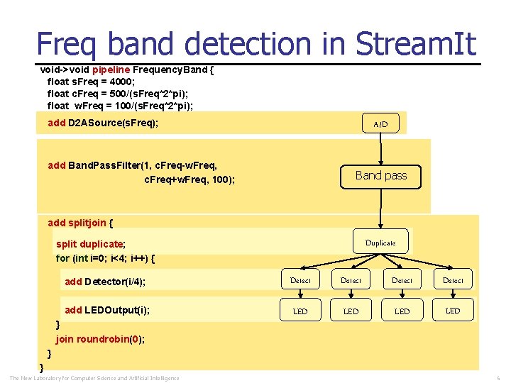
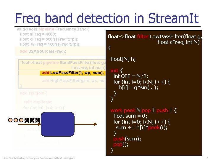
Freq band detection in Stream. It void->void pipeline Frequency. Band { float s. Freq = 4000; float c. Freq = 500/(s. Freq*2*pi); float w. Freq = 100/(s. Freq*2*pi); add D 2 ASource(s. Freq); A/D add Band. Pass. Filter(1, c. Freq-w. Freq, c. Freq+w. Freq, 100); Band pass add splitjoin { Duplicate split duplicate; for (int i=0; i<4; i++) { add Detector(i/4); Detect add LEDOutput(i); LED LED } join roundrobin(0); } } The New Laboratory for Computer Science and Artificial Intelligence 6

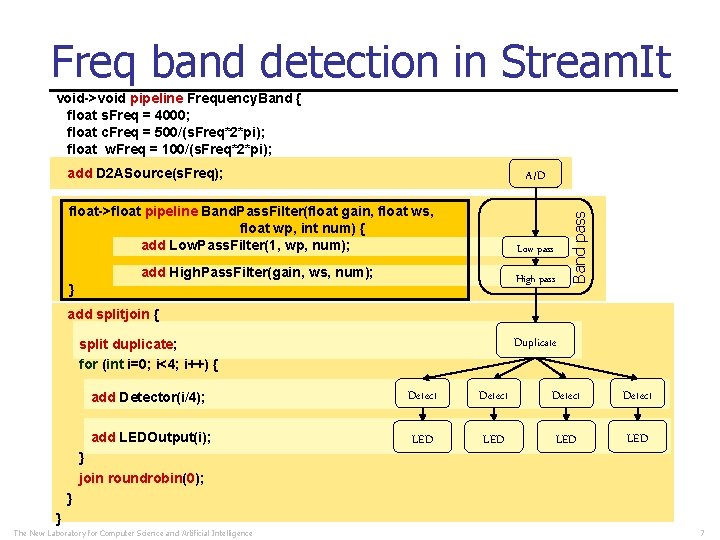
Freq band detection in Stream. It void->void pipeline Frequency. Band { float s. Freq = 4000; float c. Freq = 500/(s. Freq*2*pi); float w. Freq = 100/(s. Freq*2*pi); add D 2 ASource(s. Freq); float->float pipeline Band. Pass. Filter(float gain, float ws, float wp, int num) { add Band. Pass. Filter(1, c. Freq-w. Freq, add Low. Pass. Filter(1, wp, num); c. Freq+w. Freq, 100); add High. Pass. Filter(gain, ws, num); } Band pass A/D Low pass High pass add splitjoin { Duplicate split duplicate; for (int i=0; i<4; i++) { add Detector(i/4); Detect add LEDOutput(i); LED LED } join roundrobin(0); } } The New Laboratory for Computer Science and Artificial Intelligence 7

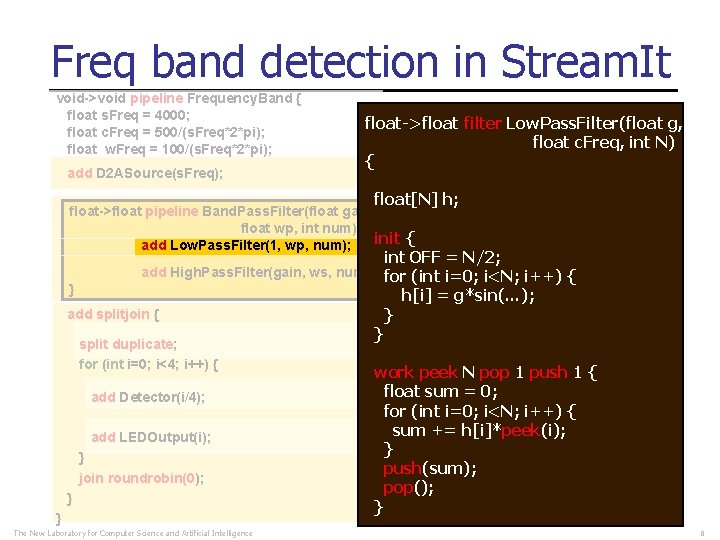
Freq band detection in Stream. It void->void pipeline Frequency. Band { float s. Freq = 4000; float c. Freq = 500/(s. Freq*2*pi); float w. Freq = 100/(s. Freq*2*pi); add D 2 ASource(s. Freq); float->float filter Low. Pass. Filter(float g, float c. Freq, int N) { A/D float[N] h; Band pass float->float pipeline Band. Pass. Filter(float gain, float ws, float->float pipeline Band. Pass. Filter(float wp, int num) { { int num) add Band. Pass. Filter(1, c. Freq-w. Freq, add Low. Pass. Filter(1, wp, num); Low. Pass. Filter(1, num); init { Low pass c. Freq+w. Freq, 100); int OFF = N/2; add High. Pass. Filter(gain, ws, num); High. Pass. Filter(gain, num); pass { for (int i=0; i<N; High i++) } } add splitjoin { split duplicate; for (int i=0; i<4; i++) { add Detector(i/4); add LEDOutput(i); } join roundrobin(0); } } The New Laboratory for Computer Science and Artificial Intelligence } } h[i] = g*sin(…); Duplicate work peek N pop 1 push 1 { float sum = Detect 0; Detect for (int i=0; i<N; i++) { sum LED+= h[i]*peek(i); LED } push(sum); pop(); } Detect LED 8

Freq band detection in Stream. It void->void pipeline Frequency. Band { float s. Freq = 4000; float c. Freq = 500/(s. Freq*2*pi); float w. Freq = 100/(s. Freq*2*pi); add D 2 ASource(s. Freq); float->float filter Low. Pass. Filter(float g, float c. Freq, int N) { A/D float[N] h; Band pass float->float pipeline Band. Pass. Filter(float gain, float ws, float wp, int num) { { add Band. Pass. Filter(1, c. Freq-w. Freq, add Low. Pass. Filter(1, wp, num); init { Low pass c. Freq+w. Freq, 100); int OFF = N/2; add High. Pass. Filter(gain, ws, num); pass { for (int i=0; i<N; High i++) } } add splitjoin { split duplicate; for (int i=0; i<4; i++) { add Detector(i/4); add LEDOutput(i); } join roundrobin(0); } } The New Laboratory for Computer Science and Artificial Intelligence } } h[i] = g*sin(…); Duplicate work peek N pop 1 push 1 { float sum = Detect 0; Detect for (int i=0; i<N; i++) { sum LED+= h[i]*peek(i); LED } push(sum); pop(); } Detect LED 9

Freq band detection on a TI DSP Band pass A/D Low pass High pass Duplicate The New Laboratory for Computer Science and Artificial Intelligence Detect LED LED 10

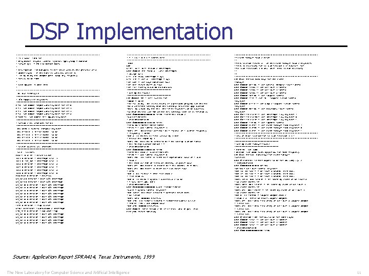
DSP Implementation ; ********************************** ; File Name: FIR 0. ASM ; Originator: Digital control systems Apps group - Houston ; Target Sys: 'C 24 x Evaluation Board ; ; Description: FIR bandpass filter which detects the presence of a ; 500 Hz signal. If the tone is detected an LED is ; lit by using the output port. Sampling Frequency ; forced to be 4 k. Hz. ; ; Last Update: 9 June 1997 ; ; **********************************. include f 240 regs. h ; ---------------------------------; I/O Mapped EVM Registers ; ---------------------------------DAC 0. set 0000 h ; Input data register for DAC 0 DAC 1. set 0001 h ; Input data register for DAC 1 DAC 2. set 0002 h ; Input data register for DAC 2 DAC 3. set 0003 h ; Input data register for DAC 3 DACUPDATE. set 0004 h ; DAC Update Register ; ---------------------------------; Variable Declarations for B 2 ; ---------------------------------. bss GPR 0, 1 ; General Purpose Register. bss DAC 0 VAL, 1 ; DAC 0 Channel Value. bss DAC 1 VAL, 1 ; DAC 1 Channel Value. bss DAC 2 VAL, 1 ; DAC 2 Channel Value. bss DAC 3 VAL, 1 ; DAC 3 Channel Value ; ---------------------------------; Vector address declarations ; ---------------------------------. sect ". vectors" RSVECT B START ; Reset Vector INT 1 B PHANTOM ; Interrupt Level 1 INT 2 B FIR_ISR ; Interrupt Level 2 INT 3 B PHANTOM ; Interrupt Level 3 INT 4 B PHANTOM ; Interrupt Level 4 INT 5 B PHANTOM ; Interrupt Level 5 INT 6 B PHANTOM ; Interrupt Level 6 RESERVED B PHANTOM ; Reserved SW_INT 8 B PHANTOM ; User S/W Interrupt SW_INT 9 B PHANTOM ; User S/W Interrupt SW_INT 10 B PHANTOM ; User S/W Interrupt SW_INT 11 B PHANTOM ; User S/W Interrupt SW_INT 12 B PHANTOM ; User S/W Interrupt SW_INT 13 B PHANTOM ; User S/W Interrupt SW_INT 14 B PHANTOM ; User S/W Interrupt SW_INT 15 B PHANTOM ; User S/W Interrupt SW_INT 16 B PHANTOM ; User S/W Interrupt TRAP B PHANTOM ; Trap vector NMINT B PHANTOM ; Non-maskable Interrupt EMU_TRAP B PHANTOM ; Emulator Trap SW_INT 20 B PHANTOM ; User S/W Interrupt SW_INT 21 B PHANTOM ; User S/W Interrupt SW_INT 22 B PHANTOM ; User S/W Interrupt SW_INT 23 B PHANTOM ; User S/W Interrupt ; ================================== ; M A I N C O D E - starts here ; ==================================. text NOP START: SETC INTM ; Disable interrupts SPLK #0002 h, IMR ; Mask all core interrupts ; except INT 2 LACC IFR ; Read Interrupt flags SACL IFR ; Clear all interrupt flags CLRC SXM ; Clear Sign Extension Mode CLRC OVM ; Reset Overflow Mode CLRC CNF ; Config Block B 0 to Data mem ; -----------------; Set up PLL Module ; -----------------LDP #00 E 0 h ; DP = 224; Address for ; 7000 h - 707 Fh ; The following line is necessary if a previous program set the PLL ; to a different setting than the settings which the application ; uses. By disabling the PLL, the CKCR 1 register can be modified ; so that the PLL can run at the new settings when it is re-enabled. SPLK #000001000001 b, CKCR 0 ; CLKMD=PLL Disable ; SYSCLK=CPUCLK/2 ; 5432109876543210 SPLK #00001011 b, CKCR 1 ; CLKIN(OSC)=10 MHz, CPUCLK=20 MHz ; CKCR 1 - Clock Control Register 1 ; Bits 7 -4 (1011)CKINF(3)-CKINF(0) - Crystal or Clock-In Frequency ; Frequency = 10 MHz ; Bit 3 (1) PLLDIV(2) - PLL divide by 2 bit ; Divide PLL input by 2 ; Bits 2 -0 (011) PLLFB(2)-PLLFB(0) - PLL multiplication ratio ; PLL Multiplication Ration = 4 ; 5432109876543210 SPLK #000011000011 b, CKCR 0 ; CLKMD=PLL Enable, SYSCLK=CPUCLK/2 ; CKCR 0 - Clock Control Register 0 ; Bits 7 -6 (11) CLKMD(1), CLKMD(0) - Operational mode of Clock ; Module ; PLL Enabled; Run on CLKIN on exiting low power mode ; Bits 5 -4 (00) PLLOCK(1), PLLOCK(0) - PLL Status. READ ONLY ; Bits 3 -2 (00) PLLPM(1), PLLPM(0) - Low Power Mode ; LPM 0 ; Bit 1 (0) ACLKENA - 1 MHz ACLK Enable ; ACLK Enabled ; Bit 0 (1) PLLPS - System Clock Prescale Value ; f(sysclk)=f(cpuclk)/2 ; 5432109876543210 SPLK #0100000011000000 b, SYSCR ; CLKOUT=CPUCLK ; SYSCR - System Control Register ; Bit 15 -14 (01) RESET 1, RESET 0 - Software Reset Bits ; No Action ; Bits 13 -8 (000000) Reserved ; Bit 7 -6 (11) CLKSRC 1, CLKSRC 0 - CLKOUT-Pin Source Select ; CPUCLK: CPU clock output mode ; Bit 5 -0 (000000) Reserved SPLK #006 Fh, WDCR ; Disable WD if VCCP=5 V (JP 5 in pos. 2 -3) KICK_DOG ; Reset Watchdog ; *-*-*-*-*-*-*-*-*-*-*-*-*-*-*-*-*-* ; - Event Manager Module Reset ; * ; -This section resets all of the Event Manager Module Registers. ; *This is necessary for silicon revsion 1. 1; however, for ; -silicon revisions 2. 0 and later, this is not necessary ; * ; ; *-*-*-*-*-*-*-*-*-*-*-*-*-*-*-*-*-* LDP #232 ; DP=232 Data Page for the Event ; Manager SPLK #0000 h, GPTCON ; Clear General Purpose Timer Control SPLK #0000 h, T 1 CON ; Clear GP Timer 1 Control SPLK #0000 h, T 2 CON ; Clear GP Timer 2 Control SPLK #0000 h, T 3 CON ; Clear GP Timer 3 Control SPLK #0000 h, COMCON ; Clear Compare Control SPLK #0000 h, ACTR ; Clear Full Compare Action Control ; Register SPLK #0000 h, SACTR ; Clear Simple Compare Action Control ; Register SPLK #0000 h, DBTCON ; Clear Dead-Band Timer Control ; Register SPLK #0 FFFFh, EVIFRA; Clear Interrupt Flag Register A SPLK #0 FFFFh, EVIFRB; Clear Interrupt Flag Register B SPLK #0 FFFFh, EVIFRC; Clear Interrupt Flag Register C SPLK #0000 h, CAPCON ; Clear Capture Control SPLK #0000 h, EVIMRA ; Clear Event Manager Mask Register A SPLK #0000 h, EVIMRB ; Clear Event Manager Mask Register B SPLK #0000 h, EVIMRC ; Clear Event Manager Mask Register C ; *-*-*-*-*-*-*-*-*-*-*-*-*-*-*-*-*-* ; End of RESET section for silicon revision 1. 1 * ; *-*-*-*-*-*-*-*-*-*-*-*-*-*-*-*-*-* ; -----------------; Set up Event Manager Module ; -----------------T 1 COMPARE. set 2500 T 1 PERIOD. set 5000 ; Sets up period for 4 k. Hz frequency LDP #232 ; DP=232, Data Page for Event Manager Addresses SPLK #T 1 COMPARE, T 1 CMPR; Compare value for 50% duty cycle ; 2109876543210 SPLK #000000101 b, GPTCON ; GPTCON - GP Timer Control Register ; Bit 15 (0) T 3 STAT - GP Timer 3 Status. READ ONLY ; Bit 14 (0) T 2 STAT - GP Timer 2 Status. READ ONLY ; Bit 13 (0) T 1 STAT - GP Timer 1 Status. READ ONLY ; Bits 12 -11 (00) T 3 TOADC - ADC start by event of GP Timer 3 ; No event starts ADC ; Bits 10 -9 (00) T 2 TOADC - ADC start by event of GP Timer 2 ; No event starts ADC ; Bits 8 -7 (00) T 1 TOADC - ADC start by event of GP Timer 1 ; No event starts ADC ; Bit 6 (1) TCOMPOE - Compare output enable ; Enable all three GP timer compare outputs ; Bits 5 -4 (01) T 3 PIN - Polarity of GP Timer 3 compare output ; Active Low ; Bits 3 -2 (01) T 2 PIN - Polarity of GP Timer 2 compare output ; Active Low ; Bits 1 -0 (01) T 1 PIN - Polarity of GP Timer 1 compare output ; Active Low SPLK #T 1 PERIOD, T 1 PR ; Period value for 2 k. Hz signal SPLK #0000 h, T 1 CNT ; Clear GP Timer 1 Counter SPLK #0000 h, T 2 CNT ; Clear GP Timer 2 Counter SPLK #0000 h, T 3 CNT ; Clear GP Timer 3 Counter ; 5432109876543210 SPLK #00010000010 b, T 1 CON Source: Application Report SPRA 414, Texas Instruments, 1999 The New Laboratory for Computer Science and Artificial Intelligence 11

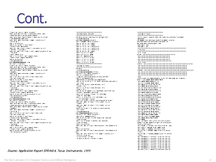
Cont. ; T 1 CON - GP Timer 1 Control Register ; Bits 15 -14(00) FREE, SOFT - Emulation Control Bits ; Stop immediately on emulation suspend ; Bits 13 -11(010) TMODE 2 -TMODE 0 - Count Mode Selection ; Continuous-Up Count Mode ; Bits 10 -8 (000) TPS 2 -TPS 0 - Input Clock Prescaler ; Divide by 1 ; Bit 7 (0) Reserved ; Bit 6 (0) TENABLE - Timer Enable ; Disable timer operations ; Bits 5 -4 (00) TCLKS 1, TCLKS 0 - Clock Source Select ; Internal Clock Source ; Bits 3 -2 (00) TCLD 1, TCLD 0 - Timer Compare Register Reload ; Condition ; When counter is 0 ; Bit 1 (1) TECMPR - Timer compare enable ; Enable timer compare operation ; Bit 0 (0) Reserved ; 5432109876543210 SPLK #00000000 b, T 2 CON ; GP Timer 2 - Not Used ; T 2 CON - GP Timer 2 Control Register ; Bits 15 -14(00) FREE, SOFT - Emulation Control Bits ; Stop immediately on emulation suspend ; Bits 13 -11(000) TMODE 2 -TMODE 0 - Count Mode Selection ; Stop/Hold ; Bits 10 -8 (000) TPS 2 -TPS 0 - Input Clock Prescaler ; Divide by 1 ; Bit 7 (0) TSWT 1 - GP Timer 1 timer enable bit ; Use own TENABLE bit ; Bit 6 (0) TENABLE - Timer Enable ; Disable timer operations ; Bits 5 -4 (00) TCLKS 1, TCLKS 0 - Clock Source Select ; Internal Clock Source ; Bits 3 -2 (00) TCLD 1, TCLD 0 - Timer Compare Register Reload ; Condition ; When counter is 0 ; Bit 1 (0) TECMPR - Timer compare enable ; Disable timer compare operation ; Bit 0 (0) SELT 1 PR - Period Register select ; Use own period register ; 5432109876543210 SPLK #00000000 b, T 3 CON ; GP Timer 3 - Not Used ; T 3 CON - GP Timer 3 Control Register ; Bits 15 -14(00) FREE, SOFT - Emulation Control Bits ; Stop immediately on emulation suspend ; Bits 13 -11(000) TMODE 2 -TMODE 0 - Count Mode Selection ; Stop/Hold ; Bits 10 -8 (000) TPS 2 -TPS 0 - Input Clock Prescaler ; Divide by 1 ; Bit 7 (0) TSWT 1 - GP Timer 1 timer enable bit ; Use own TENABLE bit ; Bit 6 (0) TENABLE - Timer Enable ; Disable timer operations ; Bits 5 -4 (00) TCLKS 1, TCLKS 0 - Clock Source Select ; Internal Clock Source ; Bits 3 -2 (00) TCLD 1, TCLD 0 - Timer Compare Register Reload ; Condition ; When counter is 0 ; Bit 1 (0) TECMPR - Timer compare enable ; Disable timer compare operation ; Bit 0 (0) SELT 1 PR - Period Register select ; Use own period register ; -----------------; Set up Digital I/O Port ; -----------------LDP #225 ; DP=225, Data Page to Configure OCRA ; 5432109876543210 SPLK #0011100000001111 b, OCRA ; OCRA - Output Control Register A ; Bit 15 (0) CRA. 15 - IOPB 7 ; Bit 14 (0) CRA. 14 - IOPB 6 ; Bit 13 (1) CRA. 13 - T 3 PWM/T 3 CMP ; Bit 12 (1) CRA. 12 - T 2 PWM/T 2 CMP ; Bit 11 (1) CRA. 11 - T 1 PWM/T 1 CMP ; Bit 10 (0) CRA. 10 - IOPB 2 ; Bit 9 (0) CRA. 9 - IOPB 1 ; Bit 8 (0) CRA. 8 - IOPB 0 ; Bits 7 -4 (0000)Reserved ; Bit 3 (1) CRA. 3 - ADCIN 8 ; Bit 2 (1) CRA. 2 - ADCIN 9 ; Bit 1 (1) CRA. 1 - ADCIN 1 ; Bit 0 (1) CRA. 0 - ADCIN 0 ; -----------------; Set up ADC Module ; -----------------LDP #224 ; 5432109876543210 SPLK #100010010000 b, ADCTRL 1 ; ADCTRL 1 - ADC Control Register 1 ; Bit 15 (1) Suspend-SOFT ; Complete Conversion before halting emulator ; Bit 14 (0) Suspend-FREE ; Operations is determined by Suspend-SOFT ; Bit 13 (0) ADCIMSTART - ADC start converting immediately ; No Action ; Bit 12 (0) ADC 2 EN - Enable/Disable ADC 2 ; Bit 11 (1) ADC 1 EN - Enable/Disable ADC 1 ; Enable ADC 1 ; Bit 10 (0) ADCCONRUN - ADC Continuous Conversion Mode ; Disable Continuous Conversion ; Bit 9 (0) ADCINTEN - Enable ADC Interrupt ; Mask ADC Interrupt ; Bit 8 (1) ADCINTFLAG - ADC Interrupt Flag ; Clear Interrupt Flag Bit ; Bit 7 (0) ADCEOC - End of Conversion Bit READ ONLY ; Bits 6 -4 (000) ADC 2 CHSEL - ADC 2 Channel Select ; Channel 8 ; Bits 3 -1 (000) ADC 1 CHSEL - ADC 1 Channel Select ; Channel 0 ; Bit 0 (0) ADCSOC - ADC Start of conversion bit ; No Action ; 5432109876543210 SPLK #0000000101 b, ADCTRL 2 ; ADCTRL 2 - ADC Control Register 2 ; Bits 15 -11 (00000)Reserved ; Bit 10 (0) ADCEVSOC - Event Manager SOC mask bit ; Mask ADCEVSOC ; Bit 9 (0) ADCEXTSOC - External SOC mask bit ; Mask ADCEXTSOC ; Bit 8 (0) Reserved ; Bits 7 -6 (00) ADCFIFO 1 - Data Register FIFO 1 Status READ ONLY ; Bit 5 (0) Reserved ; Bits 4 -3 (00) ADCFIFO 2 - Data Register FIFO 2 Status READ ONLY ; Bits 2 -0 (101) ADCPSCALE - ADC Input Clock Prescaler ; Prescale Value 16 ; SYSCLK Period = 0. 1 usec ; 0. 1 usec x 16 x 6 = 9. 6 usec >= 6 usec Source: Application Report SPRA 414, Texas Instruments, 1999 The New Laboratory for Computer Science and Artificial Intelligence ; -----------------; Set up DAC Module ; -----------------; The DAC module requires that wait states be generated for proper ; operation. LDP #0000 h ; Set Data Page Pointer to 0000 h, Block B 2 SPLK #4 h, GPR 0 ; Set Wait State Generator for OUT GPR 0, WSGR ; Program Space, 0 WS ; Date Space, 0 WS ; I/O Space, 1 WS ; ---------------------------------; MAIN LINE ; ---------------------------------. sect ". blk 0" XVALUE. word 0, 0, 0, 0, 0, 0, 0, 0, 0, 0, 0. word 0, 0, 0, 0, 0, 0. sect ". blk 1" VALUEIN. word 0, 0, 0, 0, 0, 0, 0, 0, 0, 0, 0, 0, 0, 0, 0, 0, 0 VALUEOUT. word 0, 0, 0, 0, 0, 0, 0, 0, 0, 0, 0, 0, 0, 0, 0, 0, 0. data ; Coefficients for 500 Hz Bandpass filter for 4 k. Hz Sampling Frequency BCOEFF. word 0000 h, 0002 h, 0001 h. word 0000 h, 0 FFFFh. word 0 FFFFh, 0000 h, 0002 h. word 0002 h, 0 FFFFh, 0 FFF 9 h, 0 FFF 7 h. word 0000 h, 0013 h, 0025 h, 0021 h. word 0 FFFBh, 0 FFBCh, 0 FF 90 h, 0 FFA 7 h. word 0011 h, 00 A 4 h, 00 FDh, 00 BFh. word 0 FFDEh, 0 FEC 3 h, 0 FE 2 Ah, 0 FEA 7 h. word 0033 h, 0206 h, 02 F 1 h, 0220 h. word 0 FFC 2 h, 0 FD 19 h, 0 FBD 6 h, 0 FD 05 h. word 003 Ch, 03 B 8 h, 054 Ah, 03 C 5 h. word 0 FFD 4 h, 0 FBB 4 h, 0 F 9 EAh, 0 FBADh. word 0010 h, 0484 h, 0660 h, 0484 h. word 0010 h, 0 FBADh, 0 F 9 EAh, 0 FBB 4 h. word 0 FFD 4 h, 03 C 5 h, 054 Ah, 03 B 8 h. word 003 Ch, 0 FD 05 h, 0 FBD 6 h, 0 FD 19 h. word 0 FFC 2 h, 0220 h, 02 F 1 h, 0206 h. word 0033 h, 0 FEA 7 h, 0 FE 2 Ah, 0 FEC 3 h. word 0 FFDEh, 00 BFh, 00 FDh, 00 A 4 h. word 0011 h, 0 FFA 7 h, 0 FF 90 h, 0 FFBCh. word 0 FFFBh, 0021 h, 0025 h, 0013 h. word 0000 h, 0 FFF 7 h, 0 FFF 9 h, 0 FFFFh. word 0002 h, 0000 h, 0000 h. word 0 FFFFh, 0000 h, 0000 h. word 0000 h, 0001 h, 0002 h. word 0000 h LEDS. set 000 Ch ; I/O Address for LEDS register WINDOW. set 500 ; Number of smpls to check before ; reset’g MAX values. bss LEDSOUT, 1 ; Variable for which LEDS to light. bss MAXIN, 1 ; Maximum value input value. bss MAXOUT, 1 ; Maxumum FIR result value. bss DIFFIN, 1 ; Maximum Input Value - DC Offset ; (7 ffh). bss DIFFOUT, 1 ; Maximum Output value - DC Offset ; (7 ffh). bss THRESHOLD 1, 1 ; Threshold value for 1 st LED. bss THRESHOLD 2, 1 ; Threshold value for 2 nd LED. bss THRESHOLD 3, 1 ; Threshold value for 3 rd LED. bss THRESHOLD 4, 1 ; Threshold value for 4 th LED. bss THRESHOLD 5, 1 ; Threshold value for 5 th LED. bss THRESHOLD 6, 1 ; Threshold value for 6 th LED. bss THRESHOLD 7, 1 ; Threshold value for 7 th LED. bss THRESHOLD 8, 1 ; Threshold value for 8 th LED. bss RESET_MAX, 1 ; Counter to determine when to 12

Cont. ; reset MAX values. bss TEMP, 1 ; Variable for temporary storage ; of values. text MAIN LAR AR 1, #ADCFIFO 1 ; AR 1 = ADCFIFO 1 address LAR AR 2, #ADCTRL 1 ; AR 2 = ADCTRL 1 address LAR AR 3, #BCOEFF ; AR 3 = BCOEFF address LAR AR 5, #LEDS ; AR 5 = LEDS Output LDP #232 LACC EVIFRA ; ACC = Event Module Type A Interrupt ; Flags SACL EVIFRA ; EVIFRA = ACC; Clears the current ; set flags SPLK #0080 h, EVIMRA ; Enable Timer 1 Period ; Interrupt MAR *, AR 2 ; ARP = AR 2 LACC * ; ACC = ADCTRL 1 ADD #1 ; SET BIT FOR SINGLE CONVERSION SACL *, 0, AR 1 ; STARTS ADC CONVERSION SBIT 1 T 1 CON, B 6_MSK ; Sets Bit 6 of T 1 CON; Starts ; the timer LDP #0 ; DP = 0; Addresses 0000 h - 007 Fh SPLK #0000 h, LEDSOUT ; Clear the LEDS OUT LEDSOUT, LEDS SPLK #0 E 38 h, THRESHOLD 1; Q 15 value for 1/9 SPLK #1 C 71 h, THRESHOLD 2; Q 15 value for 2/9 SPLK #2 AAAh, THRESHOLD 3; Q 15 value for 3/9 SPLK #38 E 3 h, THRESHOLD 4; Q 15 value for 4/9 SPLK #471 Ch, THRESHOLD 5; Q 15 value for 5/9 SPLK #5555 h, THRESHOLD 6; Q 15 value for 6/9 SPLK #638 Eh, THRESHOLD 7; Q 15 value for 7/9 SPLK #71 C 7 h, THRESHOLD 8; Q 15 value for 8/9 SPLK #0000 h, MAXIN ; Initialize Maxmimum input ; value SPLK #0000 h, MAXOUT ; Initialize Maximum FIR output ; value SPLK #WINDOW, RESET_MAX ; Initialize the maximum ; reset counter CLRC INTM ; Enable Interrupts WAIT B WAIT ; Wait for interrupt ; ---------------------------------; INTERRUPT SERVICE ROUTINES FOR FILTER ; ---------------------------------FIR_ISR LAR AR 4, #XVALUE+100 ; AR 4 = DATA ADDRESS MAR *, AR 1 ; ARP = AR 1 = ADCFIFO 1 LACC *, 0, AR 4 ; ACC = ADCFIFO 1; ARP = AR 4 LDP #0 ; DP = 0 ; Addresses 0000 h - 007 Fh SACL DAC 1 VAL ; DAC 1 VAL = ADCFIFO 1 RPT #7 ; Shift ADC value 8 places ; - Reduce to 8 bit value SFR ; Larger bit values produced ; large results SUB #7 Fh ; Subtract the equivalent 8 bit ; DC offset LDP #04 h ; DP = 4; Address 0200 h - 027 Fh SACL XVALUE ; XVALUE = ADCFIFO 1 / 256; LACC #0 h ; Initialize the ACCUMULATOR MPY #0 h ; Initialize the PROD REG RPT #100 ; Calculate Y MACD BCOEFF, *- ; Multiply X with B, and add APAC ; final accumulation LDP #0 RPT #7 ; Shift the result 8 places to left SFL SACH DAC 0 VAL, 1 ; DAC 0 VAL = Y * 2; shift to ; remove extra sign bit ; FIR result to output ; Multiply the values by 5/4 because the maximum gain is 4/5 LT DAC 0 VAL ; TREG = DAC 0 VAL MPY #5 ; PREG = DAC 0 VAL * 5 PAC ; ACC = PREG = DAC 0 VAL * 5 SFR ; ACC = DAC 0 VAL * 5 / 2 SFR ; ACC = DAC 0 VAL * 5 / 4 SACL DAC 0 VAL ; DAC 0 VAL = DAC 0 VAL * 5/4 LACC DAC 0 VAL ; ACC = DAC 0 VAL RPT #3 ; Shift right 4 times ; = 16 bit value to SFR ; 12 bit value because ; DAC is 12 bits ADD #7 FFh ; Add DC offset AND #0 FFFh ; Ensure 12 bits SACL DAC 0 VAL ; Store value for output on the DAC LDP #7 ; DP=7; Address for 0380 h to 03 FFh SACL VALUEOUT ; Store value to find maximum ; value of the output values LAR AR 6, #(VALUEOUT+127 -1) ; AR 6 = End of VALUE OUT ; buffer LAR AR 7, #126 ; AR 7 = 127 - 1; Number of ; values to move MAR *, AR 6 ; ARP = AR 6 SHIFT 1 DMOV *-, AR 7 ; Move all of the values in ; the VALUEOUT BANZ SHIFT 1, *-, AR 6 ; Data Buffer to the next ; higher address LDP #0 ; DP = 0; Addresses 0000 h - 007 Fh LACC DAC 1 VAL ; ACC = DAC 1 VAL = Input Value RPT #3 ; Shift the value to the ; right 4 times SFR ; Convert the value from 16 ; bits to 12 bits SACL DAC 1 VAL ; DAC 1 VAL = 12 bit value for DAC LDP #6 ; DP = 6; Addresses 0300 h - 037 Fh SACL VALUEIN ; VALUEIN = DAC 1 VAL LAR AR 6, #(VALUEIN+127 -1); AR 6 = End of VALUE IN ; buffer LAR AR 7, #126 ; AR 7 = 127 - 1; Number of ; values to move MAR *, AR 6 ; ARP = AR 6 SHIFT 2 DMOV *-, AR 7 ; Move all of the values in ; the VALUEIN BANZ SHIFT 2, *-, AR 6 ; Data Buffer to the next ; higher address ; Outputs the FIR results and the original value ; DAC 0 has the FIR results and DAC 1 has the original value LDP #0 OUT DAC 0 VAL, DAC 0 ; DAC 0 = DAC 0 VAL; FIR result on ; DAC channel 0 OUT DAC 1 VAL, DAC 1 ; DAC 1 = DAC 1 VAL; Input value ; on DAC channel 1 OUT DAC 0 VAL, DACUPDATE ; Update the values on the DAC ; Find the maximum value among VALUEIN and VALUEOUT for the LEDs LACC RESET_MAX ; ACC = RESET_MAX ; Max Reset Counter SUB #1 ; Decrement by 1 SACL RESET_MAX ; Store new value for RESET_MAX BCND NO_RESET, GT ; If not WINDOWth value, don’t ; reset counter SPLK #WINDOW, RESET_MAX ; Else reset the max reset counter SPLK #0000 h, MAXIN ; Reset the MAXIN value SPLK #0000 h, MAXOUT ; Reset the MAXOUT value NO_RESET LAR AR 6, #VALUEIN ; AR 6 = VALUEIN; Beginning of Source: Application Report SPRA 414, Texas Instruments, 1999 The New Laboratory for Computer Science and Artificial Intelligence ; Data In Buffer LAR AR 7, #127 ; AR 7 = 128 - 1; Counter to find ; max value in MAR *, AR 6 ; ARP = AR 6 FIND_MAXIN LACC *+, 0, AR 7 ; ACC = Value pointed by AR 6 SUB MAXIN ; Subtract MAXIN BCND RESUME 1, LEQ ; If the value results in a ; value less than 0, ; then the value is smaller ; than MAXIN, else the ; value is larger than MAXIN ADD MAXIN ; ACC = Value pointed by AR 6 SACL MAXIN ; Store new MAXIN value RESUME 1 BANZ FIND_MAXIN, *-, AR 6 ; If smaller than MAXIN, ; decrement loop counter ; (AR 7), move to next value in ; buffer LAR AR 7, #127 ; Since VALUEIN buffer is ; adjacent to ; VALUEOUT buffer, only AR 7 ; needs to be reset ; ARP is already AR 6 FIND_MAXOUT LACC *+, 0, AR 7 ; ACC = Value pointed by AR 6 SUB MAXOUT ; Subtract MAXOUT BCND RESUME 2, LEQ ; If the value results in a ; value less than 0, ; then the value is smaller than ; MAXOUT, els ; the value is larger than ; MAXOUT ADD MAXOUT ; ACC = Value pointed by AR 6 SACL MAXOUT ; Store new MAXOUT value RESUME 2 BANZ FIND_MAXOUT, *-, AR 6 ; If smaller than MAXOUT, ; dec loop counter (AR 7), ; move to next value in buffer ; The following section determines if the value meets the threshold ; requirement LDP #0 ; DP = 0; Addresses 0000 h to 007 Fh ; All variables used are in B 2 ; Need to remove the DC offset because if the FIR result is 0 it will ; equal 7 ffh which is already 50% of the maximum input value LACC MAXIN ; ACC = MAXIN SUB #7 FFh ; Subtract the DC offset SACL DIFFIN ; DIFFIN = MAXIN - 7 ffh LACC MAXOUT ; ACC = MACOUT SUB #7 FFh ; Subtract the DC offset SACL DIFFOUT ; DIFFOUT = MAXOUT - 7 ffh ; Check if the output exceeds the middle threshold value, THRESHOLD 4 LT DIFFIN ; TREG = DIFFIN TH 4 MPY THRESHOLD 4 ; PREG = DIFFIN * THRESHOLD 4 PAC ; ACC = PREG SACH TEMP, 1 ; TEMP = ACC*2; Shift to remove ; extra sign bit LACC TEMP ; ACC = TEMP SUB DIFFOUT ; Subtract DIFFOUT BCND ABOVE 4, LT ; If DIFFOUT is greater than ; TEMP, then the FIR result is ; greater than VALUEIN * THRESHOLD 4, ; else, it is below THRESHOLD 4 value ; Output is below THRESHOLD 4. Check if above THRESHOLD 2 BELOW 4 LT DIFFIN TH 2 MPY THRESHOLD 2 PAC SACH TEMP, 1 LACC TEMP SUB DIFFOUT BCND ABOVE 2, LT ; Output is below THRESHOLD 4 & THRESHOLD 2. Check if above THRESHOLD 1 BELOW 2 LT DIFFIN TH 1 MPY THRESHOLD 1 PAC SACH TEMP, 1 LACC TEMP SUB DIFFOUT BCND ABOVE 1, LT 13

Cont. ; Output is below THRESHOLD 4, THRESHOLD 2, & THRESHOLD 1. Turn off LEDS BELOW 1 SPLK #0000 h, LEDSOUT B OUTLEDS ; Output is below THRESHOLD 4, THRESHOLD 2, but above THRESHOLD 1. Turn ; on DS 1 ABOVE 1 SPLK #0001 h, LEDSOUT B OUTLEDS ; Output is below THRESHOLD 4, but above THRESHOLD 2. Check if above ; THRESHOLD 3 ABOVE 2 LT DIFFIN TH 3 MPY THRESHOLD 3 PAC SACH TEMP, 1 LACC TEMP SUB DIFFOUT BCND ABOVE 3, LT ; Output is below THRESHOLD 4 and THRESHOLD 3, but above THRESHOLD 2. ; Turn on DS 1 -DS 2 BELOW 3 SPLK #0003 h, LEDSOUT B OUTLEDS ; Output is below THRESHOLD 4, but above THRESHOLD 3 and THRESHOLD 2. ; Turn on DS 1 -DS 3 ABOVE 3 SPLK #0007 h, LEDSOUT B OUTLEDS ; Output is above THRESHOLD 4. Check if above THRESHOLD 6 ABOVE 4 LT DIFFIN TH 6 MPY THRESHOLD 6 PAC SACH TEMP, 1 LACC TEMP SUB DIFFOUT BCND ABOVE 6, LT ; Output is above THRESHOLD 4, but below THRESHOLD 6. Check if above ; THRESHOLD 5. BELOW 6 LT DIFFIN TH 5 MPY THRESHOLD 5 PAC SACH TEMP, 1 LACC TEMP SUB DIFFOUT BCND ABOVE 5, LT ; Output is above THRESHOLD 4, but below THRESHOLD 6 & THRESHOLD 5. Turn ; on DS 1 -DS 4 BELOW 5 SPLK #000 Fh, LEDSOUT B OUTLEDS ; Output is above THRESHOLD 4 & THRESHOLD 5, but below THRESHOLD 6. ; Turn on DS 1 -DS 5 ABOVE 5 SPLK #001 Fh, LEDSOUT B OUTLEDS ; Output is above THRESHOLD 4 & THRESHOLD 6. Check if above THRESHOLD 8. ABOVE 6 LT DIFFIN TH 8 MPY THRESHOLD 8 PAC SACH TEMP, 1 LACC TEMP SUB DIFFOUT BCND ABOVE 8, LT ; Output is above THRESHOLD 4 & THRESHOLD 6, but below THRESHOLD 8. ; Check if above THRESHOLD 7. BELOW 8 LT DIFFIN TH 7 MPY THRESHOLD 7 PAC SACH TEMP, 1 LACC TEMP SUB DIFFOUT BCND ABOVE 7, LT ; Output is above THRESHOLD 4 & THRESHOLD 6, but below THRESHOLD 8 & ; THRESHOLD 7. Turn on DS 1 -DS 6 BELOW 7 SPLK #003 Fh, LEDSOUT B OUTLEDS ; Output is above THRESHOLD 4, THRESHOLD 6, & THRESHOLD 7, but below ; THRESHOLD 8. Turn on ; DS 1 -DS 7 ABOVE 7 SPLK #007 Fh, LEDSOUT B OUTLEDS ; Output is above THRESHOLD 4, THRESHOLD 6, & THRESHOLD 8. Turn on ; DS 1 -DS 8 ABOVE 8 SPLK #00 FFh, LEDSOUT OUTLEDS OUT LEDSOUT, LEDS ; Turn on the LEDS RESTART_ADC MAR *, AR 2 ; ARP = AR 2 LACC * ; ACC = ADCTRL 1 ADD #1 h ; Set bit to restart the ADC SACL * ; Start converting next value LDP #232 LACC EVIFRA ; Clear the flag register of ; Event Manager SACL EVIFRA CLRC INTM ; ENABLE INTERRUPTS RET ; Return to main line ; ================================== ; I S R - PHANTOM ; ; Description: Dummy ISR, used to trap spurious interrupts. ; ; Modifies: ; ; Last Update: 16 -06 -95 ; ================================== PHANTOM B PHANTOM Source: Application Report SPRA 414, Texas Instruments, 1999 The New Laboratory for Computer Science and Artificial Intelligence 14

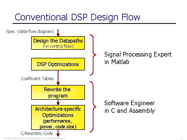
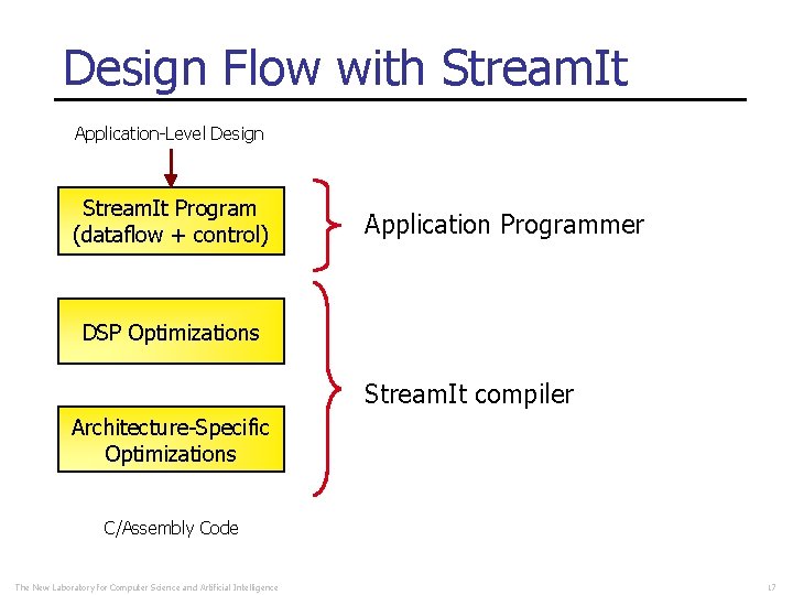
Conventional DSP Design Flow Spec. (data-flow diagram) Design the Datapaths (no control flow) DSP Optimizations Signal Processing Expert in Matlab Coefficient Tables Rewrite the program Architecture-specific Optimizations Software Engineer in C and Assembly (performance, power, code size) C/Assembly Code The New Laboratory for Computer Science and Artificial Intelligence 15

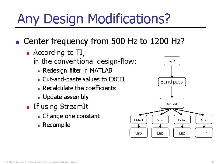
Any Design Modifications? n Center frequency from 500 Hz to 1200 Hz? n According to TI, in the conventional design-flow: n n n Redesign filter in MATLAB Cut-and-paste values to EXCEL Recalculate the coefficients Update assembly A/D Band pass Duplicate If using Stream. It n n Change one constant Recompile The New Laboratory for Computer Science and Artificial Intelligence Detect LED LED 16

Design Flow with Stream. It Application-Level Design Stream. It Program (dataflow + control) Application Programmer DSP Optimizations Stream. It compiler Architecture-Specific Optimizations C/Assembly Code The New Laboratory for Computer Science and Artificial Intelligence 17

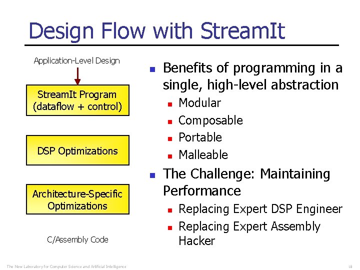
Design Flow with Stream. It Application-Level Design n Stream. It Program (dataflow + control) Benefits of programming in a single, high-level abstraction n DSP Optimizations n n Architecture-Specific Optimizations The Challenge: Maintaining Performance n n C/Assembly Code The New Laboratory for Computer Science and Artificial Intelligence Modular Composable Portable Malleable Replacing Expert DSP Engineer Replacing Expert Assembly Hacker 18

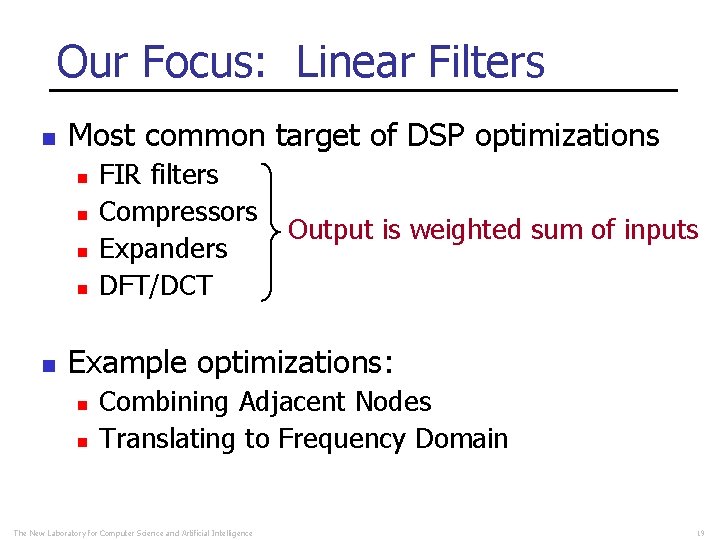
Our Focus: Linear Filters n Most common target of DSP optimizations n n n FIR filters Compressors Expanders DFT/DCT Output is weighted sum of inputs Example optimizations: n n Combining Adjacent Nodes Translating to Frequency Domain The New Laboratory for Computer Science and Artificial Intelligence 19

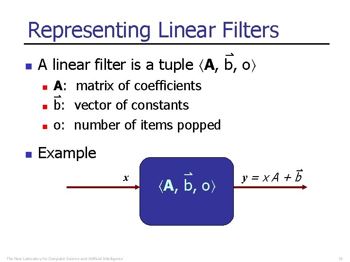
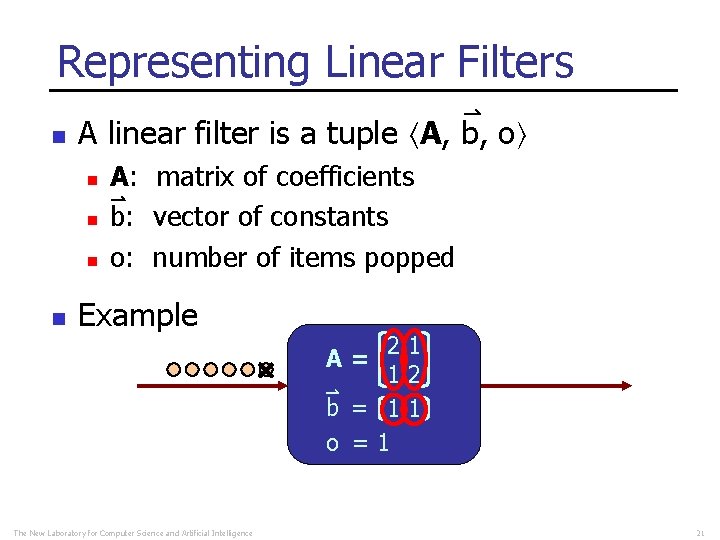
Representing Linear Filters n A linear filter is a tuple A, b, o n n A: matrix of coefficients b: vector of constants o: number of items popped Example x The New Laboratory for Computer Science and Artificial Intelligence A, b, o y= x A + b 20

Representing Linear Filters n A linear filter is a tuple A, b, o n n A: matrix of coefficients b: vector of constants o: number of items popped Example 21 12 b = 11 o =1 A= The New Laboratory for Computer Science and Artificial Intelligence 21

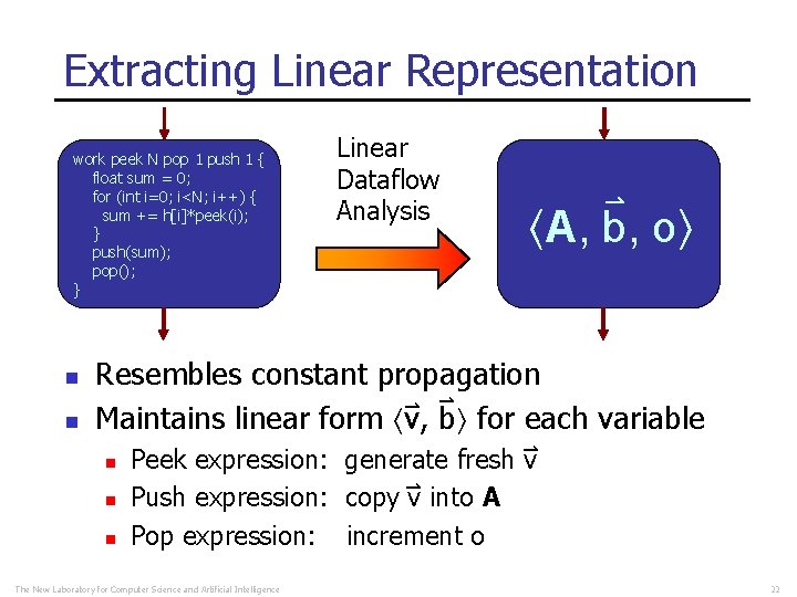
Extracting Linear Representation work peek N pop 1 push 1 { float sum = 0; for (int i=0; i<N; i++) { sum += h[i]*peek(i); } push(sum); pop(); } n n Linear Dataflow Analysis A, b, o Resembles constant propagation Maintains linear form v, b for each variable n n n Peek expression: generate fresh v Push expression: copy v into A Pop expression: increment o The New Laboratory for Computer Science and Artificial Intelligence 22

Optimizations using Linear Analysis 1) Combining adjacent linear structures 2) Shifting from time to the frequency domain 3) Selection of ‘optimal’ set of transformations The New Laboratory for Computer Science and Artificial Intelligence 23

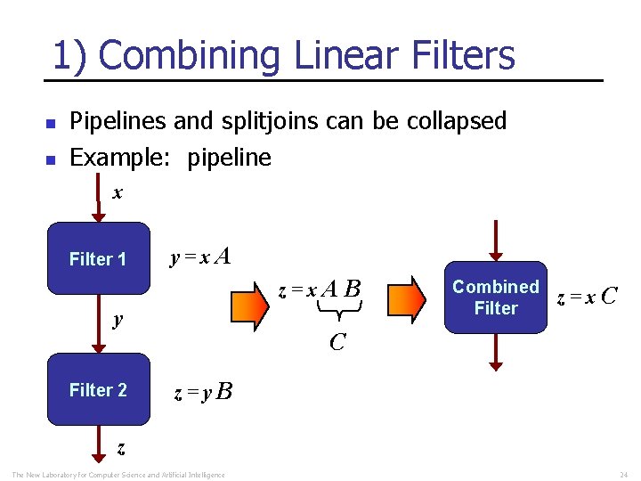
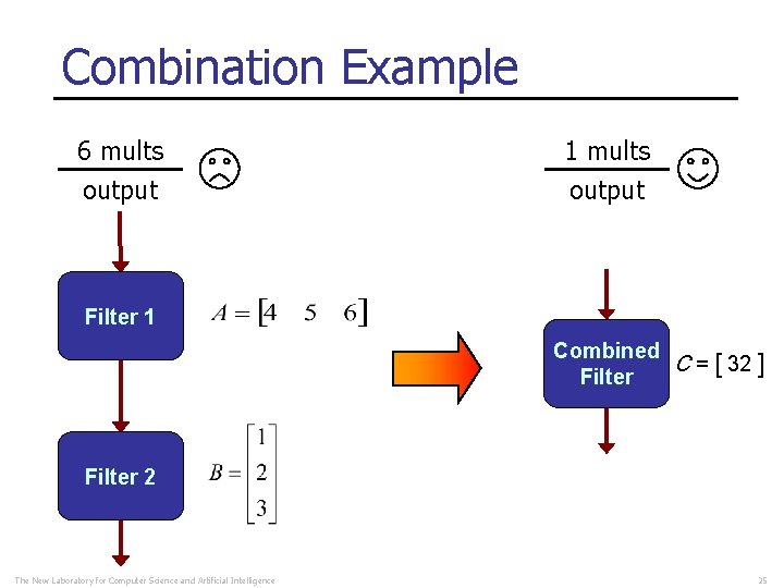
1) Combining Linear Filters n n Pipelines and splitjoins can be collapsed Example: pipeline x Filter 1 y=x. A z=x. A y Filter 2 B Combined Filter z=x. C C z=y. B z The New Laboratory for Computer Science and Artificial Intelligence 24

Combination Example 6 mults output 1 mults output Filter 1 Combined C = [ 32 ] Filter 2 The New Laboratory for Computer Science and Artificial Intelligence 25

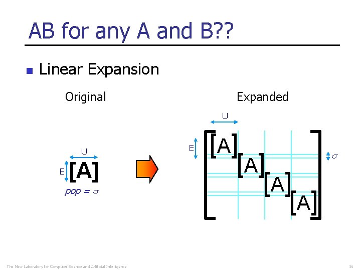
AB for any A and B? ? n Linear Expansion Original Expanded U U E [A] pop = The New Laboratory for Computer Science and Artificial Intelligence E [A] [A] 26

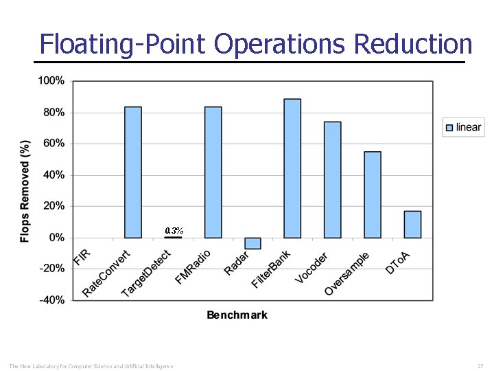
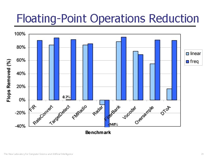
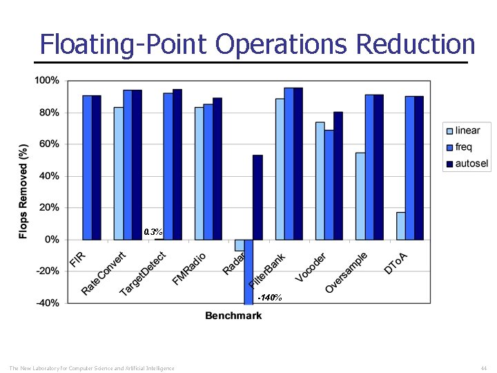
Floating-Point Operations Reduction 0. 3% The New Laboratory for Computer Science and Artificial Intelligence 27

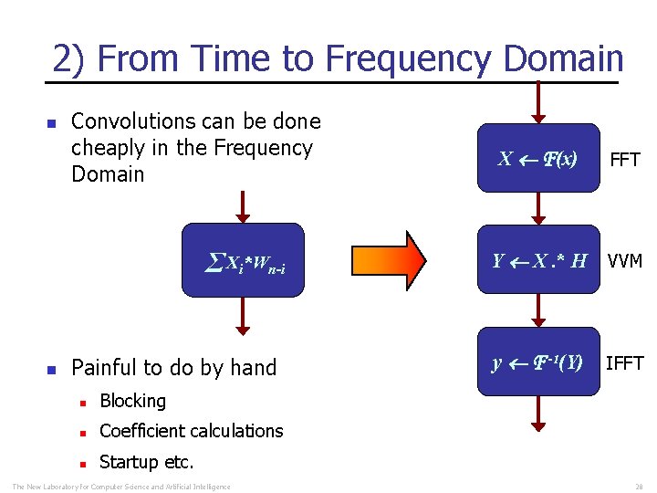
2) From Time to Frequency Domain n Convolutions can be done cheaply in the Frequency Domain Σ Xi*Wn-i n Painful to do by hand n Blocking n Coefficient calculations n Startup etc. The New Laboratory for Computer Science and Artificial Intelligence X F(x) FFT Y X. * H VVM y F -1(Y) IFFT 28

Floating-Point Operations Reduction 0. 3% -140% The New Laboratory for Computer Science and Artificial Intelligence 29

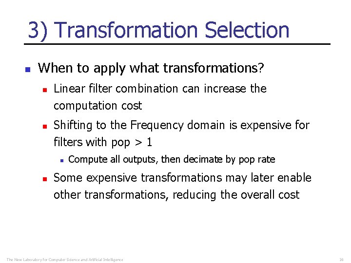
3) Transformation Selection n When to apply what transformations? n n Linear filter combination can increase the computation cost Shifting to the Frequency domain is expensive for filters with pop > 1 n n Compute all outputs, then decimate by pop rate Some expensive transformations may later enable other transformations, reducing the overall cost The New Laboratory for Computer Science and Artificial Intelligence 30

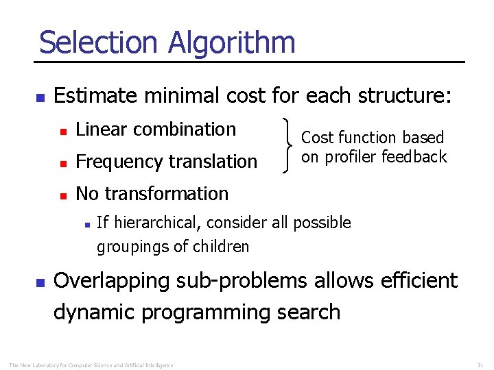
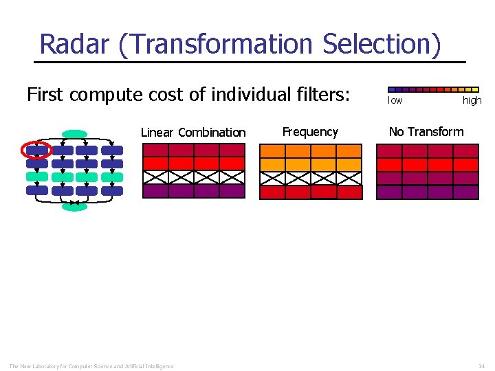
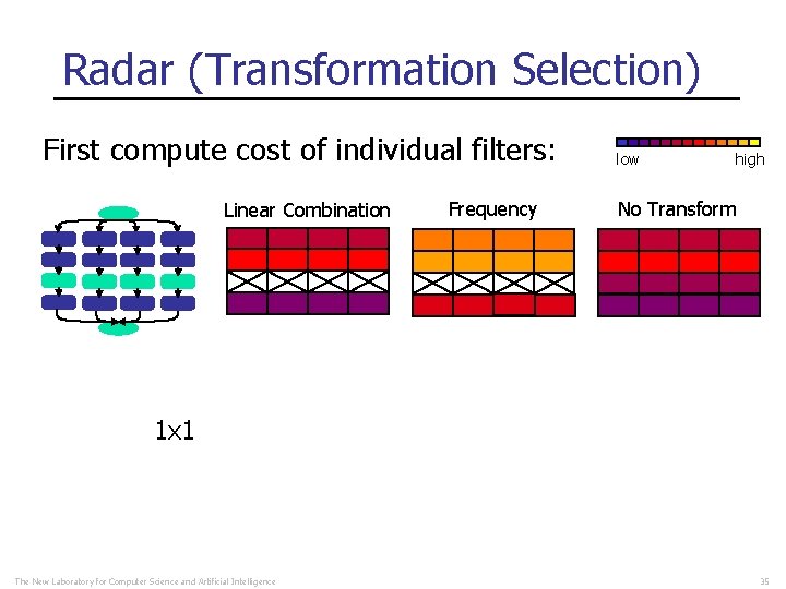
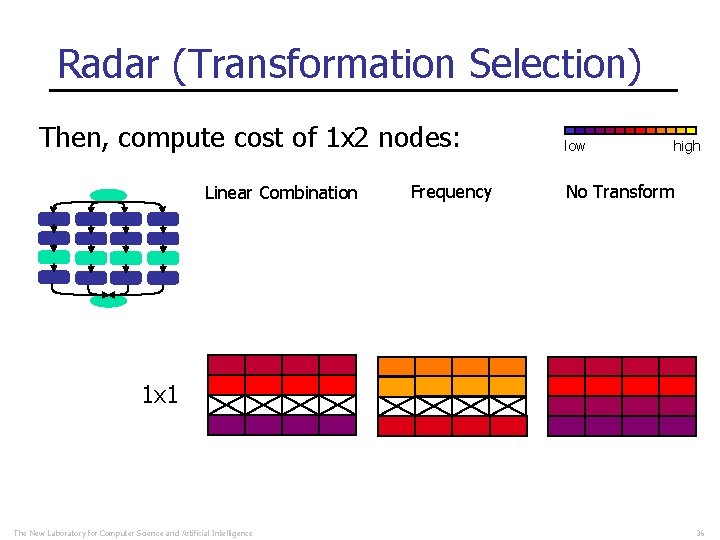
Selection Algorithm n Estimate minimal cost for each structure: n Linear combination n Frequency translation n No transformation n n Cost function based on profiler feedback If hierarchical, consider all possible groupings of children Overlapping sub-problems allows efficient dynamic programming search The New Laboratory for Computer Science and Artificial Intelligence 31

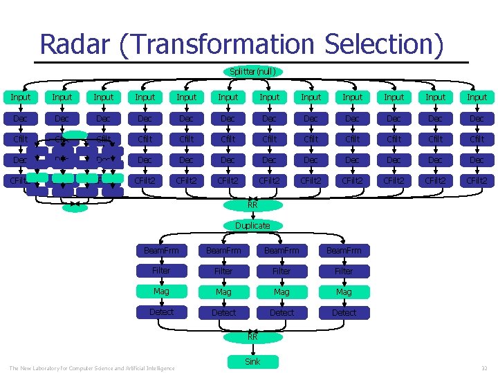
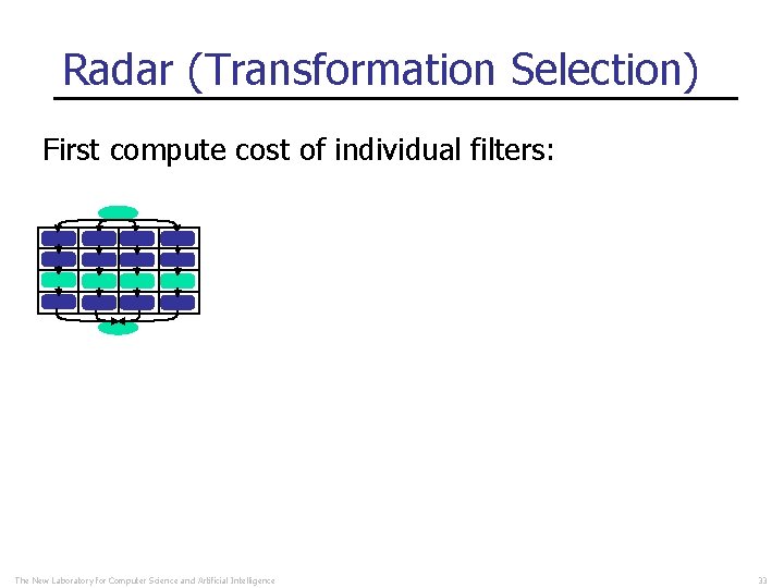
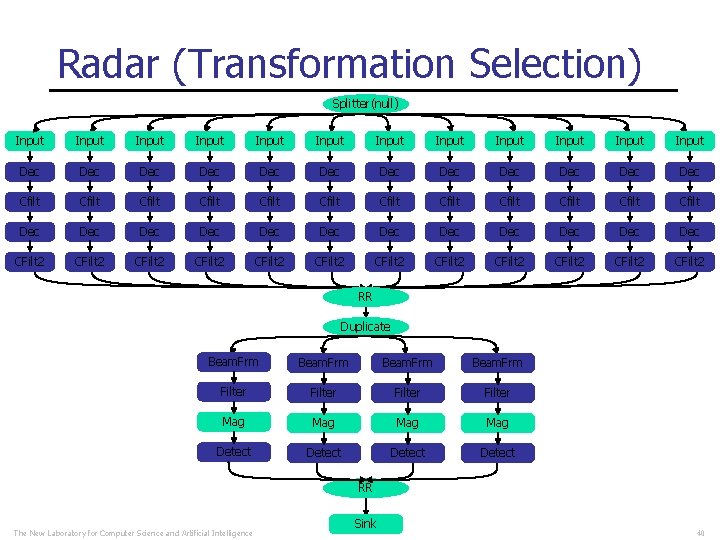
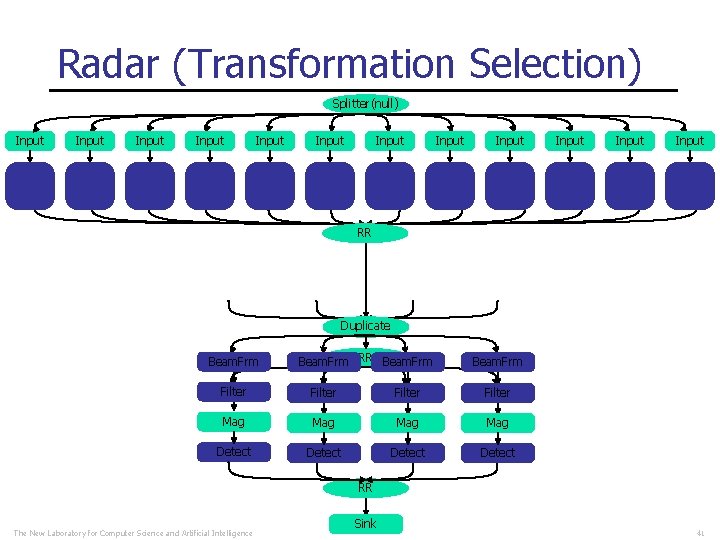
Radar (Transformation Selection) Splitter(null) Splitter Input Input Input Dec Dec Dec Cfilt Cfilt Cfilt Dec Dec Dec CFilt 2 CFilt 2 CFilt 2 RR Duplicate Beam. Frm Filter Mag Mag Detect RR The New Laboratory for Computer Science and Artificial Intelligence Sink 32

Radar (Transformation Selection) First compute cost of individual filters: The New Laboratory for Computer Science and Artificial Intelligence 33

Radar (Transformation Selection) First compute cost of individual filters: Linear Combination The New Laboratory for Computer Science and Artificial Intelligence Frequency low high No Transform 34

Radar (Transformation Selection) First compute cost of individual filters: Linear Combination Frequency low high No Transform 1 x 1 The New Laboratory for Computer Science and Artificial Intelligence 35

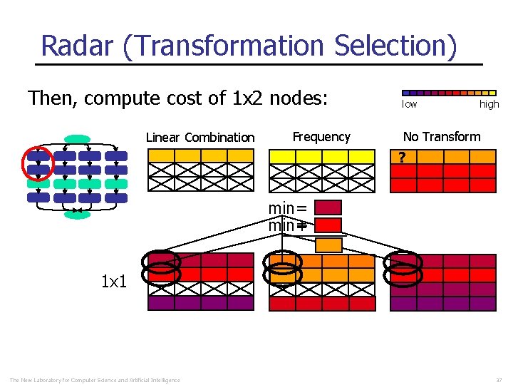
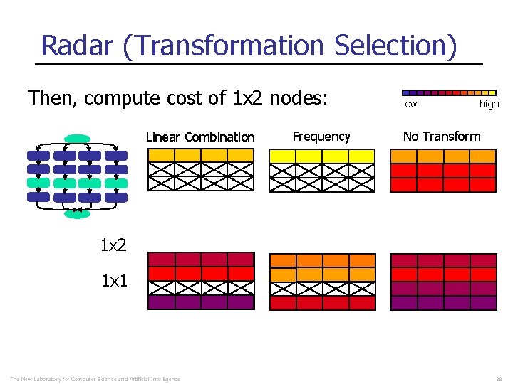
Radar (Transformation Selection) Then, compute cost of 1 x 2 nodes: Linear Combination Frequency low high No Transform 1 x 1 The New Laboratory for Computer Science and Artificial Intelligence 36

Radar (Transformation Selection) Then, compute cost of 1 x 2 nodes: Linear Combination Frequency low high No Transform ? min= + 1 x 1 The New Laboratory for Computer Science and Artificial Intelligence 37

Radar (Transformation Selection) Then, compute cost of 1 x 2 nodes: Linear Combination Frequency low high No Transform 1 x 2 1 x 1 The New Laboratory for Computer Science and Artificial Intelligence 38

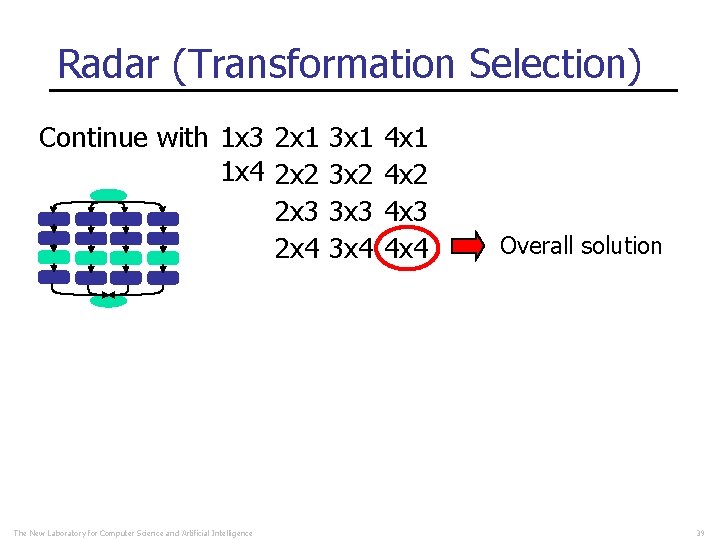
Radar (Transformation Selection) Continue with 1 x 3 2 x 1 3 x 1 1 x 4 2 x 2 3 x 2 2 x 3 3 x 3 2 x 4 3 x 4 The New Laboratory for Computer Science and Artificial Intelligence 4 x 1 4 x 2 4 x 3 4 x 4 Overall solution 39

Radar (Transformation Selection) Splitter(null) Splitter Input Input Input Dec Dec Dec Cfilt Cfilt Cfilt Dec Dec Dec CFilt 2 CFilt 2 CFilt 2 RR Duplicate Beam. Frm Filter Mag Mag Detect RR The New Laboratory for Computer Science and Artificial Intelligence Sink 40

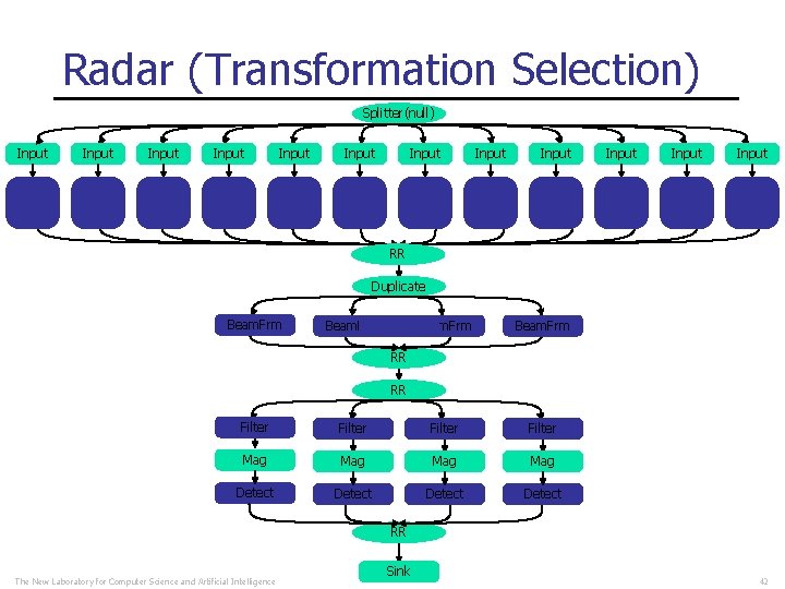
Radar (Transformation Selection) Splitter(null) Splitter Input Input Input RR Duplicate RR Beam. Frm Filter Mag Mag Detect RR The New Laboratory for Computer Science and Artificial Intelligence Sink 41

Radar (Transformation Selection) Splitter(null) Splitter Input Input Input RR Duplicate Beam. Frm RR RR Filter Mag Mag Detect RR The New Laboratory for Computer Science and Artificial Intelligence Sink 42

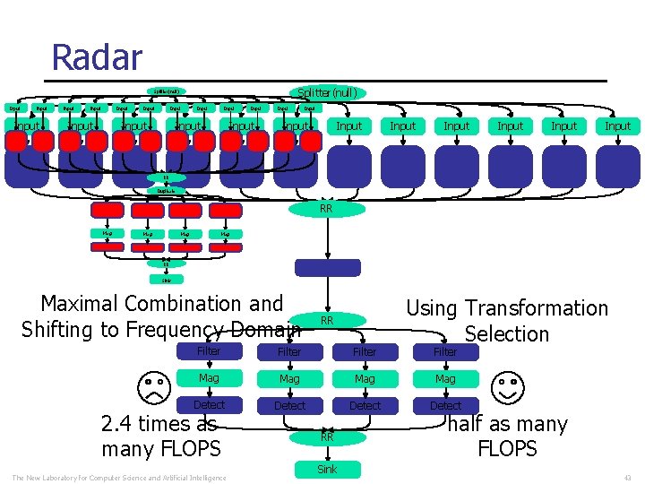
Radar (Transformation Selection) Splitter(null) Splitter Input Input Input Input Input Input RR Duplicate RR Mag Mag RR Sink Maximal Combination and Shifting to Frequency Domain RR Using Transformation Selection Filter Mag Mag Detect 2. 4 times as many FLOPS The New Laboratory for Computer Science and Artificial Intelligence RR Sink Filter half as many FLOPS 43

Floating-Point Operations Reduction 0. 3% -140% The New Laboratory for Computer Science and Artificial Intelligence 44

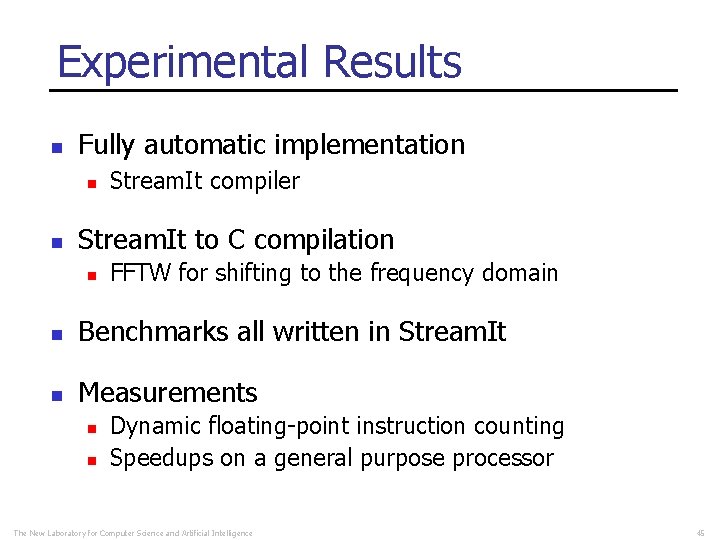
Experimental Results n Fully automatic implementation n n Stream. It compiler Stream. It to C compilation n FFTW for shifting to the frequency domain n Benchmarks all written in Stream. It n Measurements n n Dynamic floating-point instruction counting Speedups on a general purpose processor The New Laboratory for Computer Science and Artificial Intelligence 45

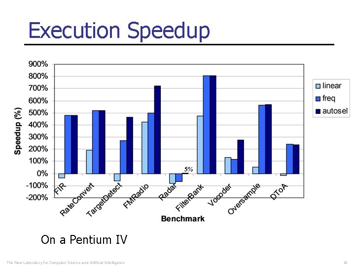
Execution Speedup 5% On a Pentium IV The New Laboratory for Computer Science and Artificial Intelligence 46

Related Work n SPIRAL/SPL (Püschel et. al) n n FFTW (Friego et. al) n n n Wicked fast FFT ADE (Covell, MIT Ph. D Thesis, 1989) Affine Analysis (Karr, Acta Informatica, 1976) n n Automatic derivation of DSP transforms Affine relationships among variables of a program Linear Analysis (Cousot, Halbwatchs, POPL, 1978) n Automatic discovery of linear restraints among variables of a program The New Laboratory for Computer Science and Artificial Intelligence 47

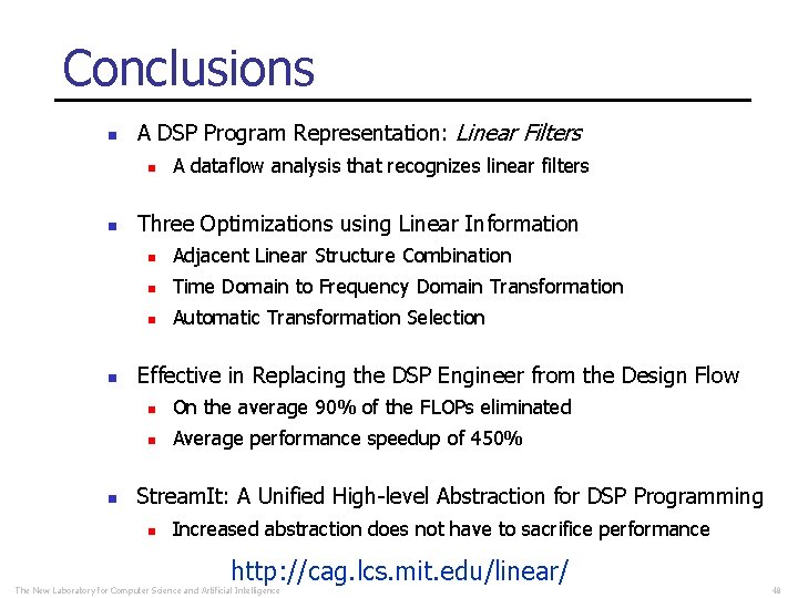
Conclusions n A DSP Program Representation: Linear Filters n n A dataflow analysis that recognizes linear filters Three Optimizations using Linear Information n Adjacent Linear Structure Combination n Time Domain to Frequency Domain Transformation n Automatic Transformation Selection Effective in Replacing the DSP Engineer from the Design Flow n On the average 90% of the FLOPs eliminated n Average performance speedup of 450% Stream. It: A Unified High-level Abstraction for DSP Programming n Increased abstraction does not have to sacrifice performance http: //cag. lcs. mit. edu/linear/ The New Laboratory for Computer Science and Artificial Intelligence 48