Leveraging ApplicationLevel Requirements in the Design of a


![Input Data – Traffic Pattern Bandwidth demands [Mb/s] Point-to-point timing requirements [n. Sec] 'R' Input Data – Traffic Pattern Bandwidth demands [Mb/s] Point-to-point timing requirements [n. Sec] 'R'](https://slidetodoc.com/presentation_image_h2/840f00c98f07800d19efa455c8f883cf/image-13.jpg)



- Slides: 24

Leveraging Application-Level Requirements in the Design of a No. C for a 4 G So. C – a Case Study Rudy Beraha, Isask’har (Zigi) Walter, Israel Cidon, Avinoam Kolodny Technion – Israel Institute of Technology Qualcomm Corp. Research and Development, San Diego, California March, 2010

Outline n Network on-Chip (No. C) § Introduction § Design Process n No. C Design § A Case Study 2

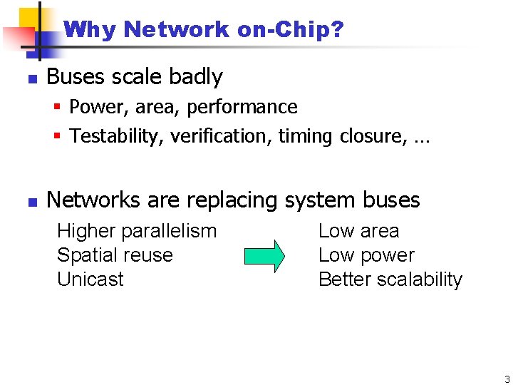
Why Network on-Chip? n Buses scale badly § Power, area, performance § Testability, verification, timing closure, … n Networks are replacing system buses Higher parallelism Spatial reuse Unicast Low area Low power Better scalability 3

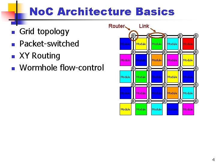
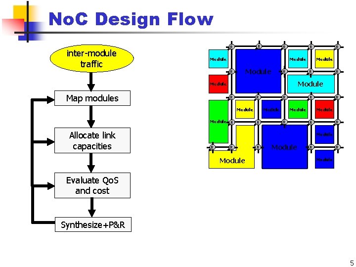
No. C Architecture Basics n n Grid topology Packet-switched XY Routing Wormhole flow-control Router Link R Module R R Module R Module Module R R R R Module Module R R Module 4

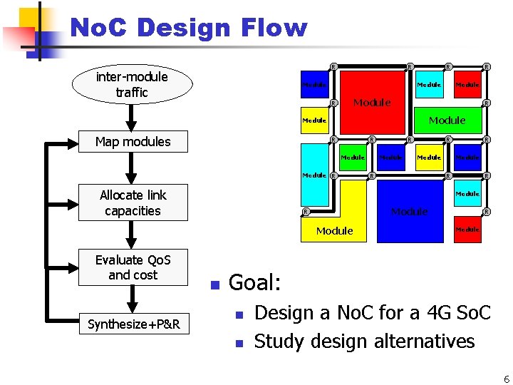
No. C Design Flow inter-module traffic R R R Module Module R Allocate link capacities Module R Module Map modules R R Module R Module R R Module Evaluate Qo. S and cost Synthesize+P&R 5

No. C Design Flow R inter-module traffic R Module Module R R Module R Allocate link capacities Synthesize+P&R R Module Module R Module Evaluate Qo. S and cost Module R Map modules R n R Module Goal: n n Design a No. C for a 4 G So. C Study design alternatives 6

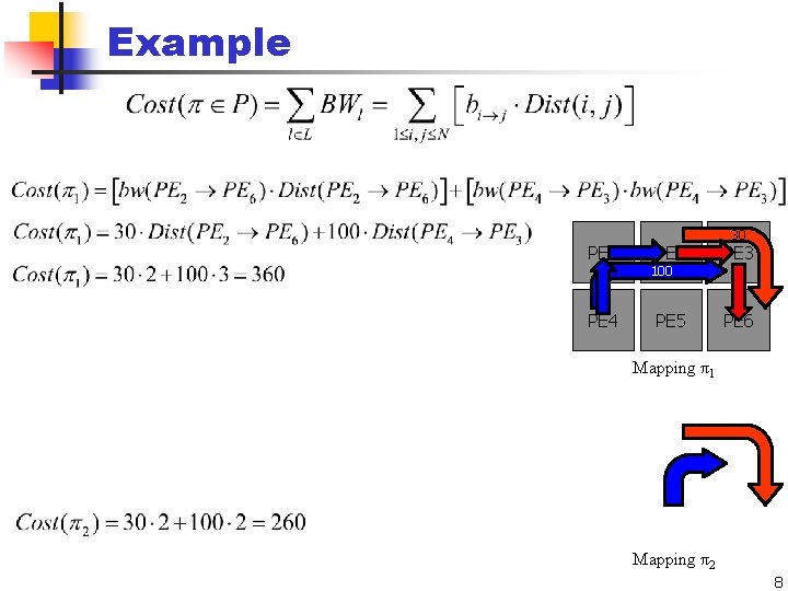
Why is Mapping Important? n Typical modeling § Latency and dynamic power proportional to distance § Dynamic power consumed by the No. C: Cost of mapping π 7

Example PE 1 PE 2 30 PE 3 100 PE 4 PE 5 PE 6 Mapping π1 Mapping π2 8

Outline n n Network on-Chip (No. C) No. C Design – a Case Study § Mapping § Link capacity allocation § Results 9

A Case Study… n Approached by Qualcomm R&D § Got a real, 4 G Modem So. C design to analyze! n Very few No. Cs for real systems are described in the literature 10

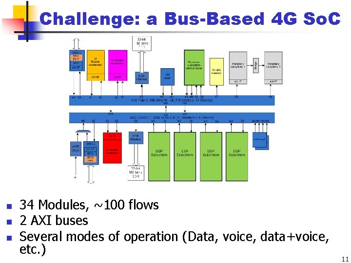
Challenge: a Bus-Based 4 G So. C n n n 34 Modules, ~100 flows 2 AXI buses Several modes of operation (Data, voice, data+voice, etc. ) 11

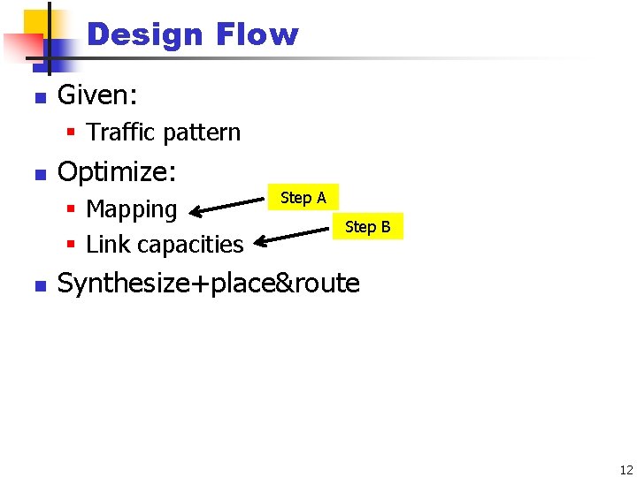
Design Flow n Given: § Traffic pattern n Optimize: § Mapping § Link capacities n Step A Step B Synthesize+place&route 12
![Input Data Traffic Pattern Bandwidth demands Mbs Pointtopoint timing requirements n Sec R Input Data – Traffic Pattern Bandwidth demands [Mb/s] Point-to-point timing requirements [n. Sec] 'R'](https://slidetodoc.com/presentation_image_h2/840f00c98f07800d19efa455c8f883cf/image-13.jpg)
Input Data – Traffic Pattern Bandwidth demands [Mb/s] Point-to-point timing requirements [n. Sec] 'R' is for read operations, 'W' is for write operations n Traditional P 2 P traffic requirements 13

Mapping Optimization - Goal n Minimize power subject to performance constraints Static power n Dynamic power Captures dynamic power and area (static power) 14

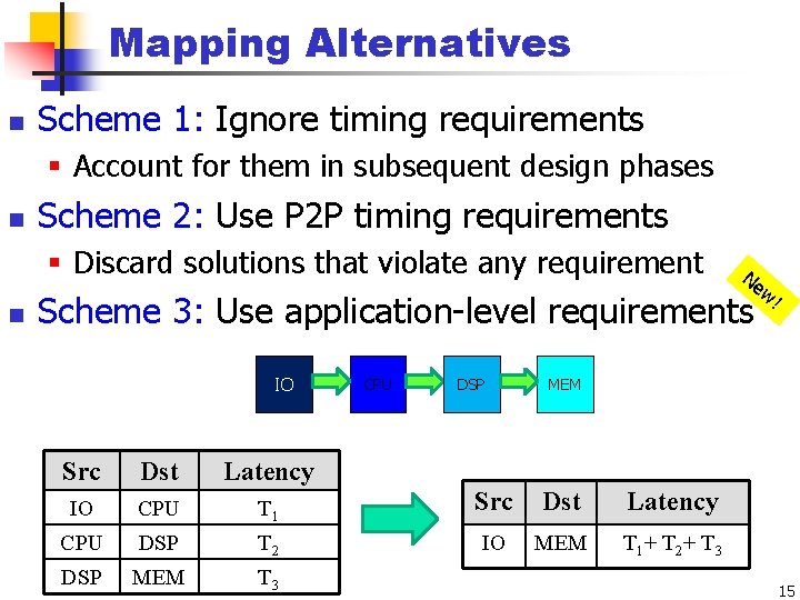
Mapping Alternatives n Scheme 1: Ignore timing requirements § Account for them in subsequent design phases n Scheme 2: Use P 2 P timing requirements § Discard solutions that violate any requirement n Ne Scheme 3: Use application-level requirements IO CPU DSP w! MEM Src Dst Latency IO CPU T 1 Src Dst Latency CPU DSP T 2 IO MEM T 1 + T 2 + T 3 DSP MEM T 3 15

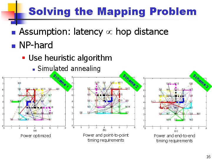
Solving the Mapping Problem n n Assumption: latency hop distance NP-hard § Use heuristic algorithm n Simulated annealing Sc he m Power optimized e Sc Sc he he m 1 Power and point-to-point timing requirements e m 2 e 3 Power and end-to-end timing requirements 16

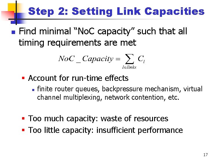
Step 2: Setting Link Capacities n Find minimal “No. C capacity” such that all timing requirements are met § Account for run-time effects n finite router queues, backpressure mechanism, virtual channel multiplexing, network contention, etc. § Too much capacity: waste of resources § Too little capacity: insufficient performance 17

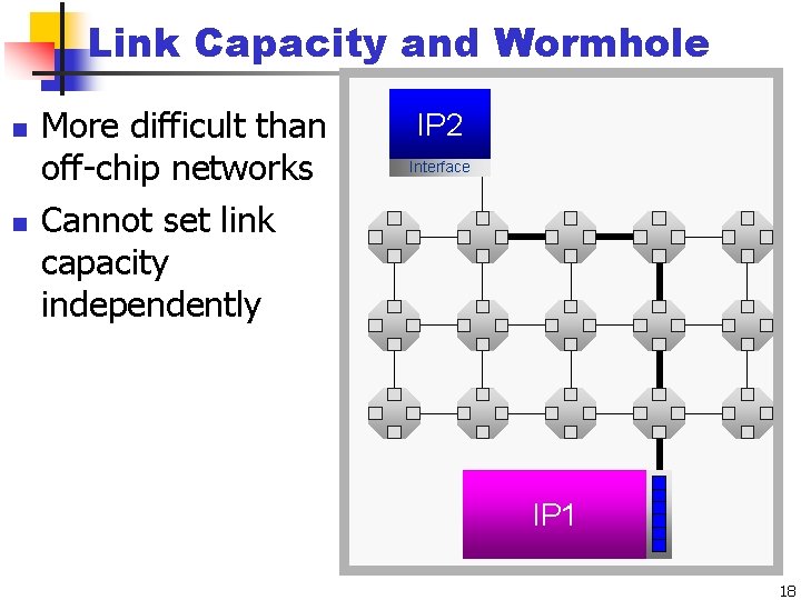
Link Capacity and Wormhole n More difficult than off-chip networks Cannot set link capacity independently IP 2 Interface IP 1 Interface n 18

Capacity Allocation Alternatives n Scheme 1: Uniform link capacity § Simulation based n Scheme 2: Individually tuned, heuristic-based § Simulation based n Result: 12 No. Cs to compare (3 mappings)*(2 allocation schemes)*(2 VC configurations) 19

Outline n n Network on-Chip (No. C) No. C Design – a Case Study § Mapping § Link capacity allocation § Results 20

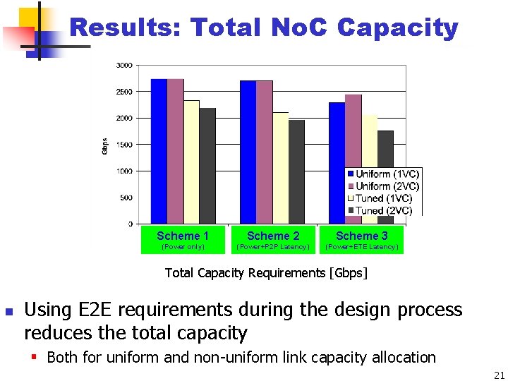
Results: Total No. C Capacity Scheme 1 Scheme 2 Scheme 3 (Power only) (Power+P 2 P Latency) (Power+ETE Latency) Total Capacity Requirements [Gbps] n Using E 2 E requirements during the design process reduces the total capacity § Both for uniform and non-uniform link capacity allocation 21

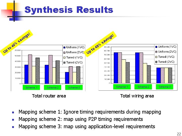
Synthesis Results ! s ng ! gs n i v vi Up to 0% sa % 4 Up Scheme 1 Scheme 2 Total router area n n n Scheme 3 to 49 sa Scheme 1 Scheme 2 Scheme 3 Total wiring area Mapping scheme 1: Ignore timing requirements during mapping Mapping scheme 2: map using P 2 P timing requirements Mapping scheme 3: map using application-level requirements 22

Conclusions and Future Work n Evaluated the benefit of mapping using application-level requirements § Rather than P 2 P constraints n n Using two link capacity allocation schemes Real application § Meaningful savings n To do § Analyze place&route results § Compare to a bus-based implementation 23

Leveraging Application-Level Requirements in the Design of a No. C Thank you! Questions? zigi@tx. technion. ac. il QNo. C Research Group 24