Lessons Learned The Hard Way FPGA PCB Integration
Lessons Learned The Hard Way: FPGA PCB Integration Challenges Dave Brady & Bruce Riggins
Agenda n n Design Overview Design Challenge Summary Lessons Learned Suggested Strategies Brady/Riggins Page 2 MAPLD 2005/P 131
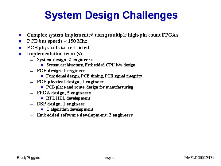
System Design Challenges n n Complex system implemented using multiple high-pin count FPGAs PCB bus speeds > 150 Mhz PCB physical size restricted Implementation team (s) — System design, 2 engineers n — PCB design, 1 engineer n — RTL HDL development DSP design, 1 engineer n — PCB place and route, design for manufacturing FPGA design, 5 engineers n — Functional design, PCB timing, PCB signal integrity PCB physical design, 1 engineer n — System architecture, Embedded CPU h/w design C algorithm development Embedded software development, 2 engineers Brady/Riggins Page 3 MAPLD 2005/P 131
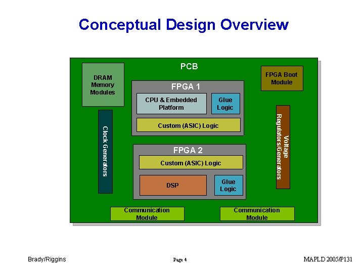
Conceptual Design Overview PCB DRAM Memory Modules FPGA 1 CPU & Embedded Platform Glue Logic FPGA 2 Custom (ASIC) Logic Communication Module Glue Logic Voltage Regulators/Generators Clock Generators Custom (ASIC) Logic DSP Brady/Riggins FPGA Boot Module Communication Module Page 4 MAPLD 2005/P 131
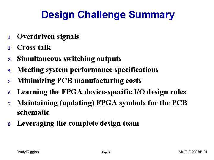
Design Challenge Summary 1. 2. 3. 4. 5. 6. 7. 8. Overdriven signals Cross talk Simultaneous switching outputs Meeting system performance specifications Minimizing PCB manufacturing costs Learning the FPGA device-specific I/O design rules Maintaining (updating) FPGA symbols for the PCB schematic Leveraging the complete design team Brady/Riggins Page 5 MAPLD 2005/P 131
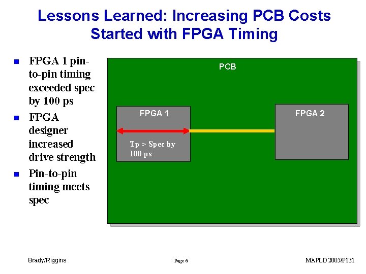
Lessons Learned: Increasing PCB Costs Started with FPGA Timing n n n FPGA 1 pinto-pin timing exceeded spec by 100 ps FPGA designer increased drive strength Pin-to-pin timing meets spec Brady/Riggins PCB FPGA 1 FPGA 2 Tp > Spec by 100 ps Page 6 MAPLD 2005/P 131

Increasing PCB Costs Induced Signal Ringing on PCB (contd. ) n n Increasing drive strength on FPGA 1 output pin induced PCB signal ringing PCB engineer identified Brady/Riggins PCB FPGA 1 FPGA 2 Tp < Spec Page 7 MAPLD 2005/P 131
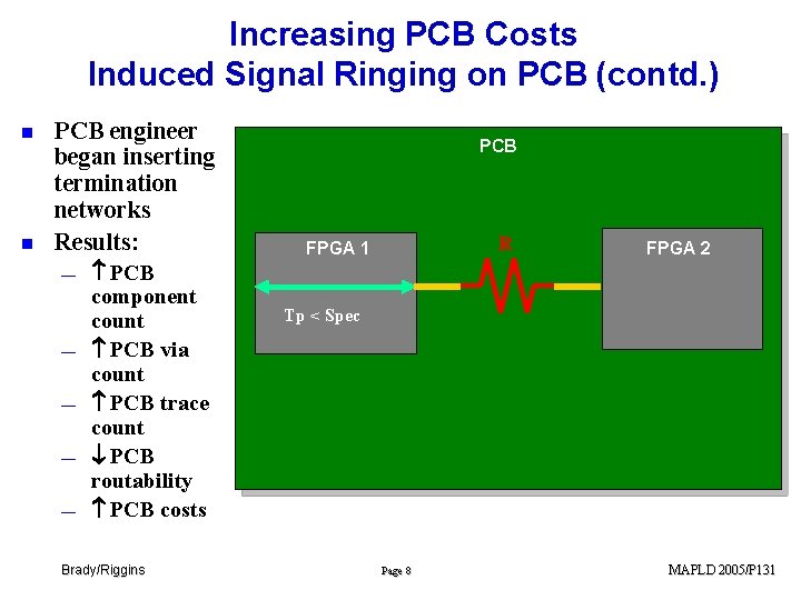
Increasing PCB Costs Induced Signal Ringing on PCB (contd. ) n n PCB engineer began inserting termination networks Results: — — — PCB component count PCB via count PCB trace count PCB routability PCB costs Brady/Riggins PCB R FPGA 1 FPGA 2 Tp < Spec Page 8 MAPLD 2005/P 131
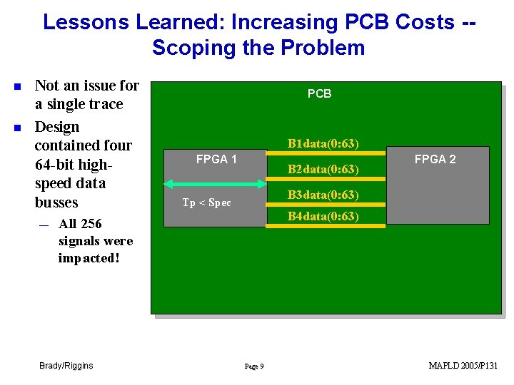
Lessons Learned: Increasing PCB Costs -Scoping the Problem n n Not an issue for a single trace Design contained four 64 -bit highspeed data busses — PCB B 1 data(0: 63) FPGA 1 B 2 data(0: 63) B 3 data(0: 63) Tp < Spec B 4 data(0: 63) All 256 signals were impacted! Brady/Riggins FPGA 2 Page 9 MAPLD 2005/P 131
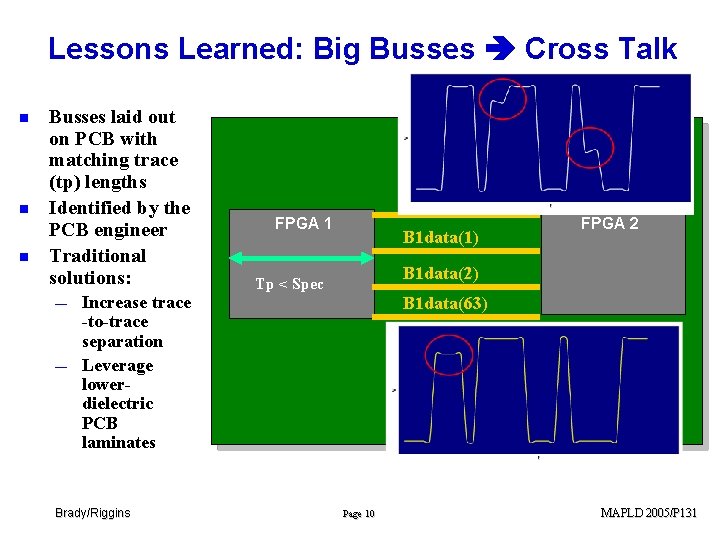
Lessons Learned: Big Busses Cross Talk n n n Busses laid out on PCB with matching trace (tp) lengths Identified by the PCB engineer Traditional solutions: — — Increase trace -to-trace separation Leverage lowerdielectric PCB laminates Brady/Riggins PCB B 1 data(0) FPGA 1 B 1 data(1) FPGA 2 B 1 data(2) Tp < Spec B 1 data(63) Page 10 MAPLD 2005/P 131
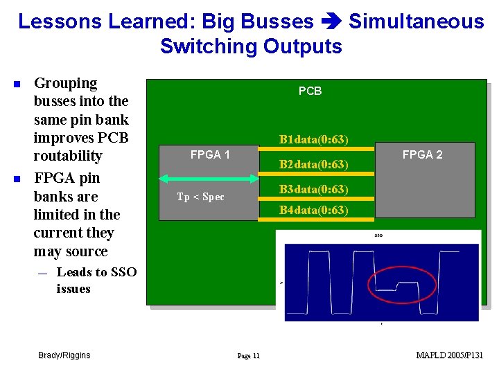
Lessons Learned: Big Busses Simultaneous Switching Outputs n n Grouping busses into the same pin bank improves PCB routability FPGA pin banks are limited in the current they may source — PCB B 1 data(0: 63) FPGA 1 B 2 data(0: 63) FPGA 2 B 3 data(0: 63) Tp < Spec B 4 data(0: 63) Leads to SSO issues Brady/Riggins Page 11 MAPLD 2005/P 131
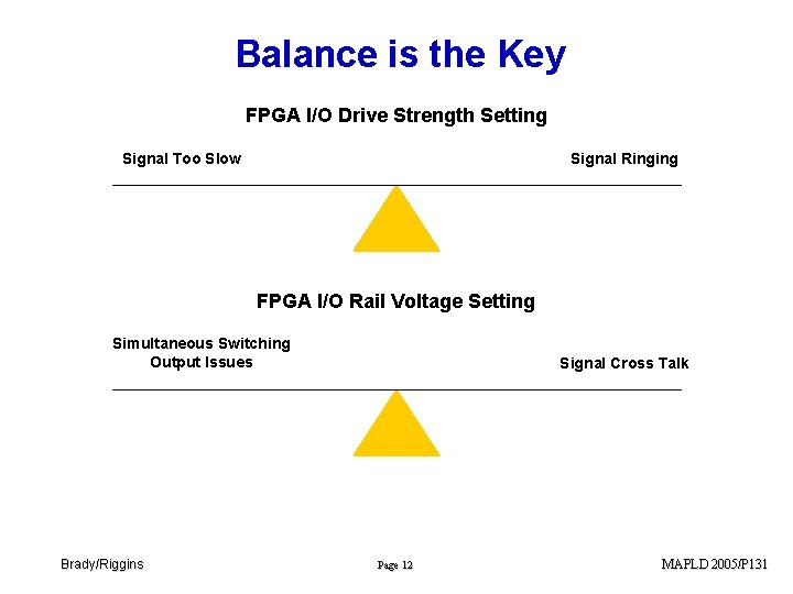
Balance is the Key FPGA I/O Drive Strength Setting Signal Too Slow Signal Ringing FPGA I/O Rail Voltage Setting Simultaneous Switching Output Issues Brady/Riggins Signal Cross Talk Page 12 MAPLD 2005/P 131
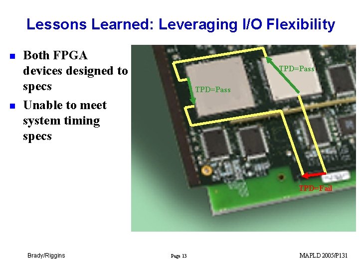
Lessons Learned: Leveraging I/O Flexibility n n Both FPGA devices designed to specs Unable to meet system timing specs TPD=Pass TPD=Fail Brady/Riggins Page 13 MAPLD 2005/P 131
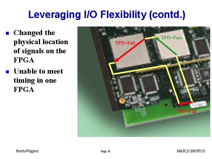
Leveraging I/O Flexibility (contd. ) n n Changed the physical location of signals on the FPGA Unable to meet timing in one FPGA TPD=Pass TPD=Fail Brady/Riggins Page 14 MAPLD 2005/P 131
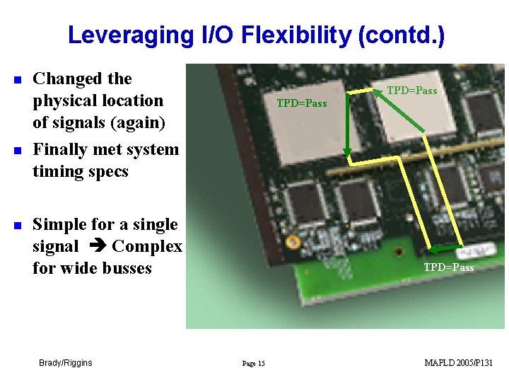
Leveraging I/O Flexibility (contd. ) n n n Changed the physical location of signals (again) Finally met system timing specs TPD=Pass Simple for a single signal Complex for wide busses Brady/Riggins TPD=Pass Page 15 MAPLD 2005/P 131
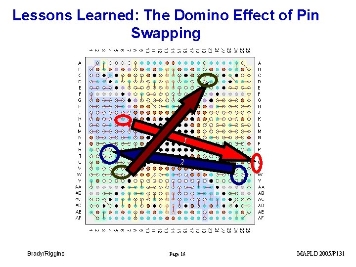
Lessons Learned: The Domino Effect of Pin Swapping 3 1 2 Brady/Riggins Page 16 MAPLD 2005/P 131
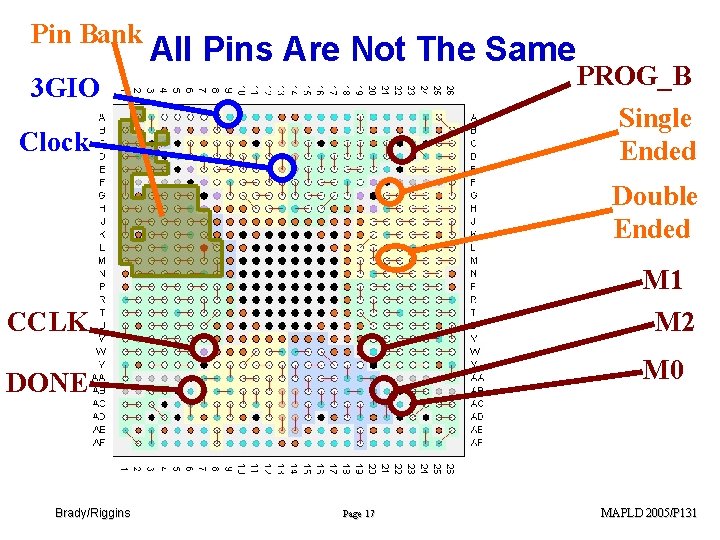
Pin Bank All Pins Are Not The Same 3 GIO Clock PROG_B Single Ended Double Ended CCLK M 1 M 2 DONE M 0 Brady/Riggins Page 17 MAPLD 2005/P 131
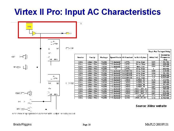
Virtex II Pro: Input AC Characteristics Source: Xilinx website Brady/Riggins Page 18 MAPLD 2005/P 131
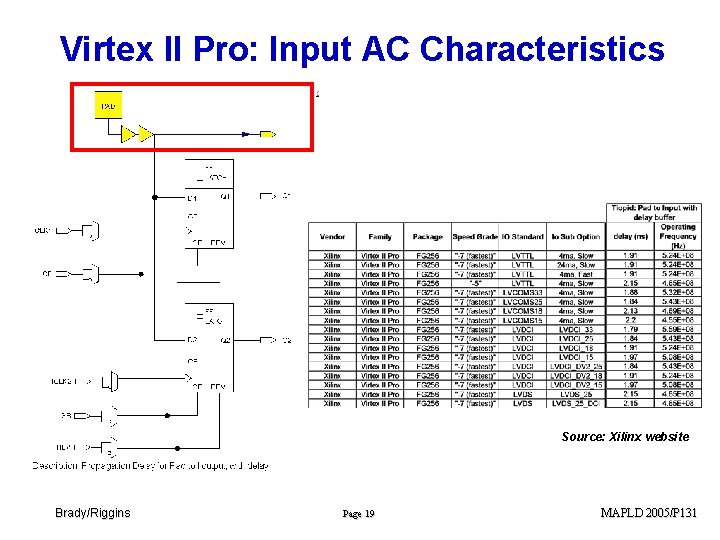
Virtex II Pro: Input AC Characteristics Source: Xilinx website Brady/Riggins Page 19 MAPLD 2005/P 131
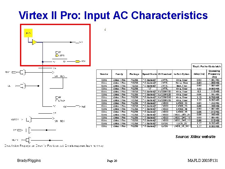
Virtex II Pro: Input AC Characteristics Source: Xilinx website Brady/Riggins Page 20 MAPLD 2005/P 131
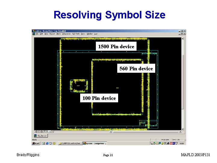
Resolving Symbol Size 1500 Pin device 560 Pin device 100 Pin device Brady/Riggins Page 21 MAPLD 2005/P 131
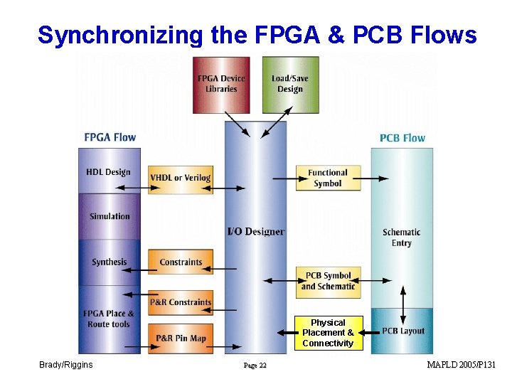
Synchronizing the FPGA & PCB Flows Physical Placement & Connectivity Brady/Riggins Page 22 MAPLD 2005/P 131
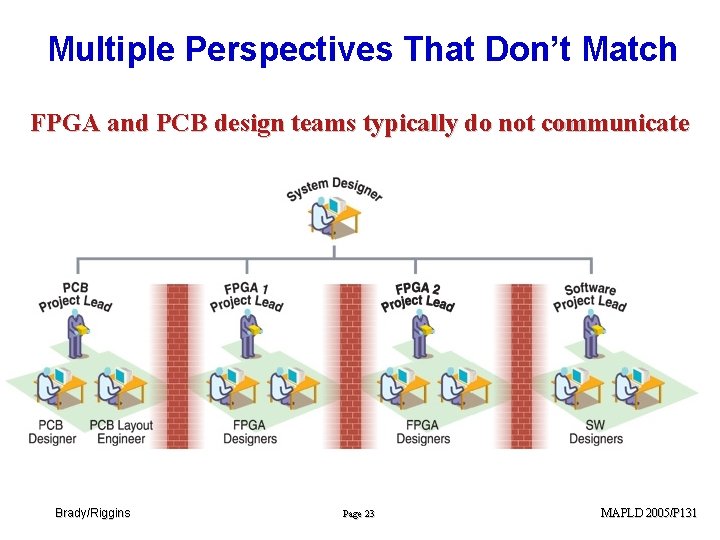
Multiple Perspectives That Don’t Match FPGA and PCB design teams typically do not communicate Brady/Riggins Page 23 MAPLD 2005/P 131
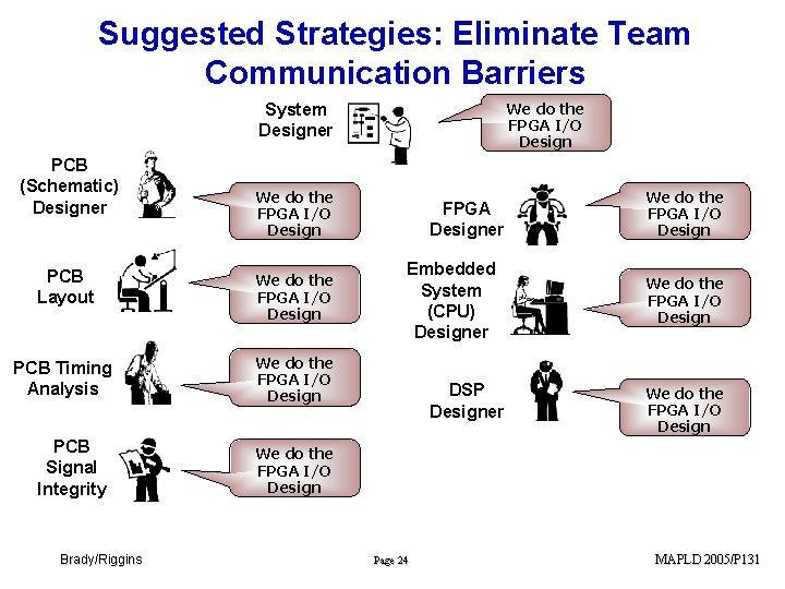
Suggested Strategies: Eliminate Team Communication Barriers We do the FPGA I/O Design System Designer PCB (Schematic) Designer We do the FPGA I/O Design PCB Layout We do the FPGA I/O Design PCB Timing Analysis We do the FPGA I/O Design PCB Signal Integrity Brady/Riggins FPGA Designer Embedded System (CPU) Designer DSP Designer We do the FPGA I/O Design Page 24 MAPLD 2005/P 131
General Tips & Tricks n Leverage Signal Integrity “What if” Analysis Early — — — n Run Signal Integrity Analysis on the PCB Design — — Some signal termination is un-avoidable Minimize PCB size Reduced PCB costs Leveraging Gigabit Transceivers Reduces PCB Traces BUT — — — n Interactive part of the normal design process NOT a design verification “check box” Leverage Embedded Resistors — n Anticipate signal ringing, cross talk, ground bounce, etc. Develop system constraints to minimize PCB components Make trade-offs at the system level GHz signals High-Speed (& cost) PCB laminates Introduces additional PCB components (clock generators, voltage regulators, etc) Introduces additional termination topology requirements Re-partition the FPGA Design to Optimize PCB Performance — — — Alternative to leveraging Gigabit transceivers Will not work for every design Worked for this design Brady/Riggins Page 25 MAPLD 2005/P 131
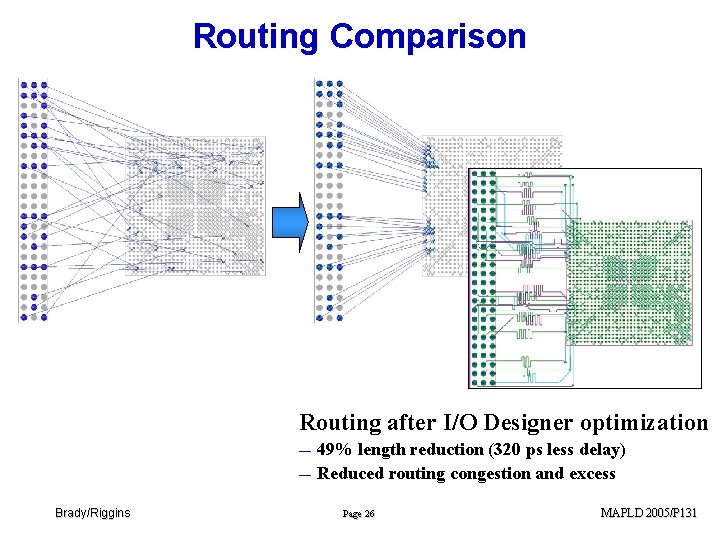
Routing Comparison Routing after I/O Designer optimization — — Brady/Riggins 49% length reduction (320 ps less delay) Reduced routing congestion and excess Page 26 MAPLD 2005/P 131
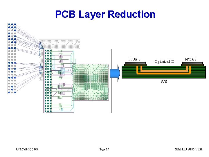
PCB Layer Reduction FPGA 1 Optimized IO FPGA 2 PCB Brady/Riggins Page 27 MAPLD 2005/P 131
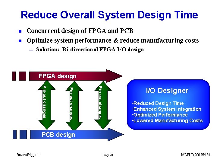
Reduce Overall System Design Time n n Concurrent design of FPGA and PCB Optimize system performance & reduce manufacturing costs — Solution: Bi-directional FPGA I/O design FPGA design Pin-out changes as -ou t n sig Brady/Riggins Pin-out changes PCB design I/O Designer • Reduced Design Time • Enhanced System Integration • Optimized Performance • Lowered Manufacturing Costs PCB design Page 28 MAPLD 2005/P 131
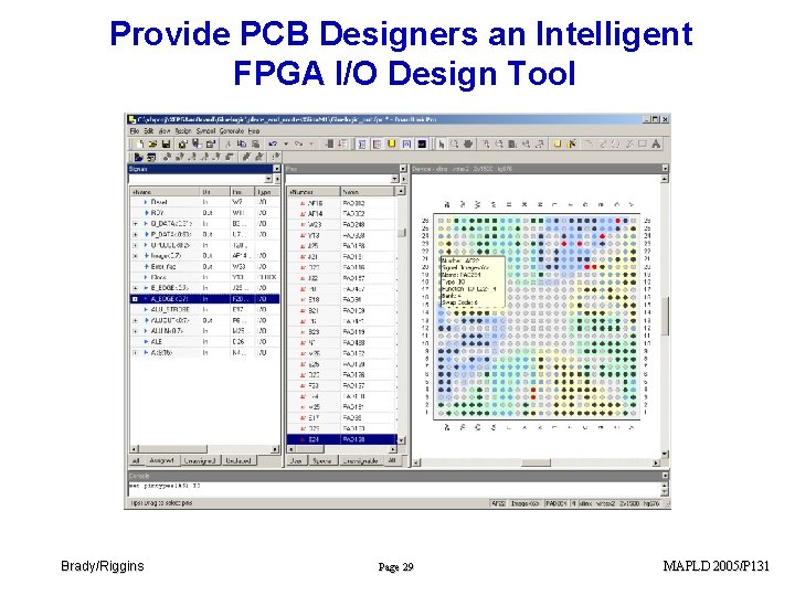
Provide PCB Designers an Intelligent FPGA I/O Design Tool Brady/Riggins Page 29 MAPLD 2005/P 131
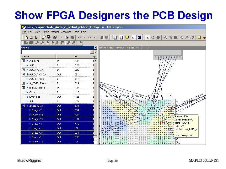
Show FPGA Designers the PCB Design Brady/Riggins Page 30 MAPLD 2005/P 131
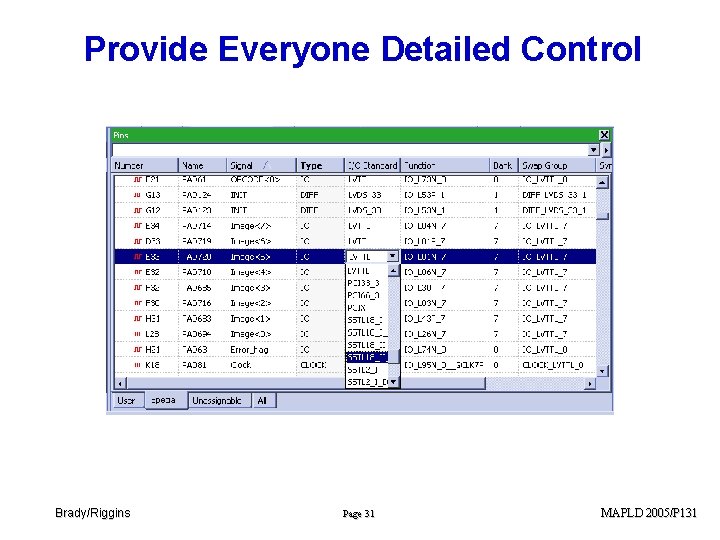
Provide Everyone Detailed Control Brady/Riggins Page 31 MAPLD 2005/P 131
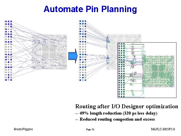
Automate Pin Planning Routing after I/O Designer optimization — — Brady/Riggins 49% length reduction (320 ps less delay) Reduced routing congestion and excess Page 32 MAPLD 2005/P 131
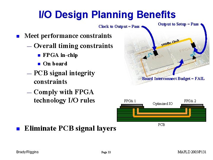
I/O Design Planning Benefits Clock to Output = Pass n Meet performance constraints — Overall timing constraints n n lock hz C 100 M FPGA in-chip On board PCB signal integrity constraints — Comply with FPGA technology I/O rules — n Board Interconnect Budget = FAIL FPGA 1 Eliminate PCB signal layers Brady/Riggins Output to Setup = Pass Page 33 Optimized IO FPGA 2 PCB MAPLD 2005/P 131
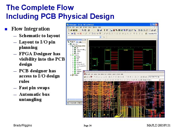
The Complete Flow Including PCB Physical Design n Flow Integration — — — Schematic to layout Layout to I/O pin planning FPGA Designer has visibility into the PCB designer has access to I/O design rules Fast pin swaps Automatic bus untangling Brady/Riggins Page 34 MAPLD 2005/P 131
- Slides: 34