LES PROPRIETES PARTICULIERES DES RUBANS SUPRACONDUCTEURS P Bernstein

LES PROPRIETES PARTICULIERES DES RUBANS SUPRACONDUCTEURS P. Bernstein 1, Y. Thimont 1 and C. Mc. Loughlin 1, 2 CRISMAT (UMR-CNRS 6508) -ENSICAEN and Université de Caen. Basse Normandie, Boulevard du Maréchal Juin F 14050 Caen cedex, France 2 National Centre for Plasma Science and Technology, School of Physical Sciences, Dublin City University, Glasnevin, Dublin 9, Ireland 1
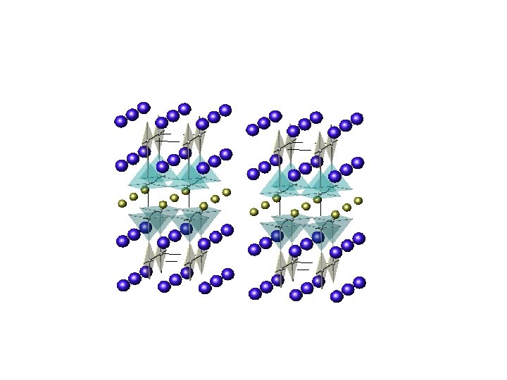
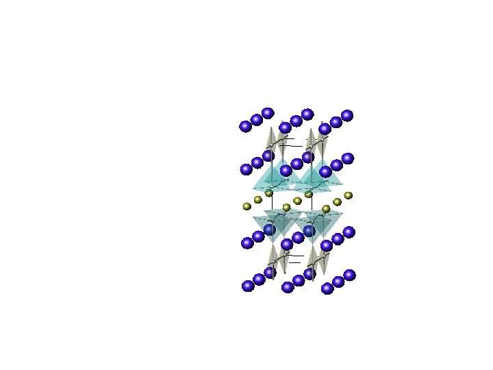
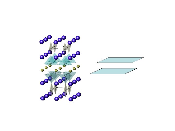
 YBa 2 Cu 3 O 7 -d (YBCO)")
COATED CONDUCTORS (2 G HTS TAPES) YBa 2 Cu 3 O 7 -d (YBCO) FAMILY

APPLICATIONS COMING SOON…

SUPERCONDUCTING CABLES FOR POWER TRANSPORTATION

SUPERCONDUCTING TRANSFORMERS P=63 MVA
 V=5 dm 3 E (k. J)")
Superconducting Magnetic Energy Storage (SMES) V=5 dm 3 E (k. J)

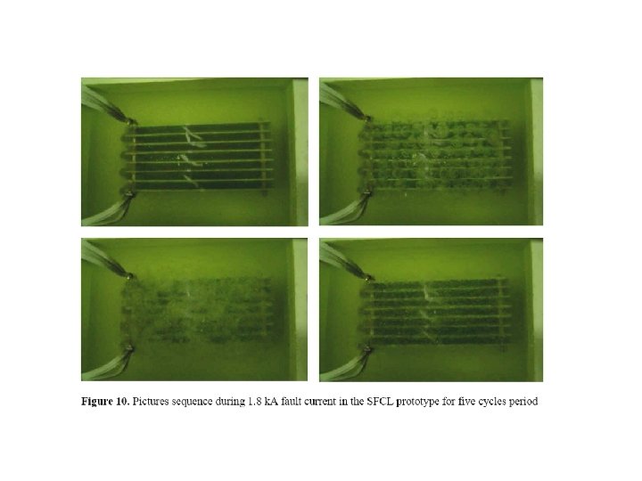
SUPERCONDUCTING FAULT CURRENT LIMITERS

COMING SOON….

EXAMPLE : SUPERCONDUCTING FAULT CURRENT LIMITERS

LES PROPRIETES PARTICULIERES DES RUBANS SUPRACONDUCTEURS • La densité de courant critique et l’existence d’un possible gradient de température critique • Le comportement au-delà du courant critique

La densité de courant critique et l’existence d’un possible gradient de température critique

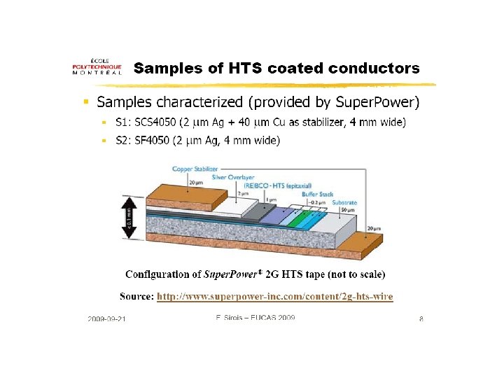
Nb. N M. E. Gershenzon and V. N. Gubankov Pi’sma Zh. Eksp. Teor. Fiz 32, 236 (1980) Super. Power SF 4050

La densité de courant critique et l’existence d’un possible gradient de température critique • La mesure magnétique de la densité de courant critique en fonction de la température • Comparaison entre des rubans de différents fabricants • Détermination de la distribution de Tc le long de la profondeur des films

SQUID magnetic moment measurement L w d 1 5 L w d 2 w L d 3 d 4

Surface Critical Current Determination L w * * E. H. Brandt and M. Indenbom, Phys. Rev. B 48, 12893 (1993) *Critical Current Measurement in HTS YBa. Cu. O ribbons, Th. Lécrevisse et al. ASC 2010

MEASURED COATED CONDUCTORS • 1 - American Superconductor • 2 – Super. Power • 3 - Theva

SURFACE CRITICAL CURRENT DENSITY

WHAT MAKES THE DIFFERENCE BETWEEN THE SAMPLES ?

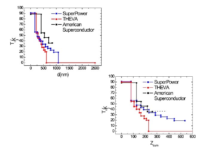
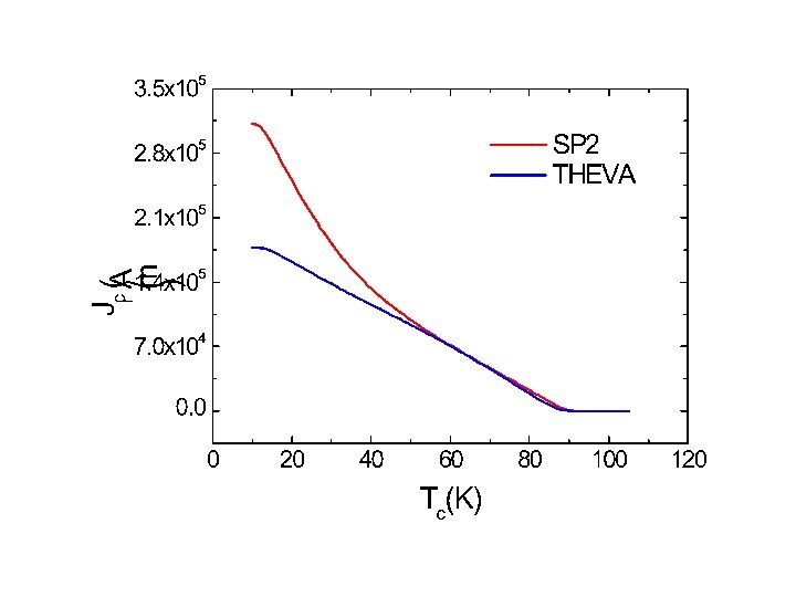
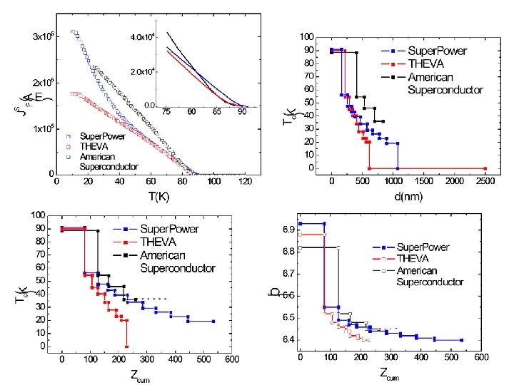
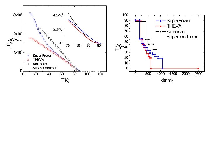
CRITICAL CURRENT DENSITY AT 5 K OF COATED CONDUCTORS

SURFACE CRITICAL CURRENT DENSITY AT T=5 K
 OF NOWADAYS COATED")
COMPARISON WITH THE SURFACE CRITICAL CURRENT DENSITY AT LOW TEMPERATURE (Tmin) OF NOWADAYS COATED CONDUCTORS
 SAMPLE dph (nm) ds(nm) American 1 mm Superconductor 0.")
1 - SUPERCONDUCTING THICKNESS (ds) SAMPLE dph (nm) ds(nm) American 1 mm Superconductor 0. 9 mm Theva 2. 5 mm 0. 6 mm Super. Power 1 mm

CRITICAL CURRENT DENSITY AT 77 K OF COATED CONDUCTORS

SURFACE CRITICAL CURRENT DENSITY AT 77 K

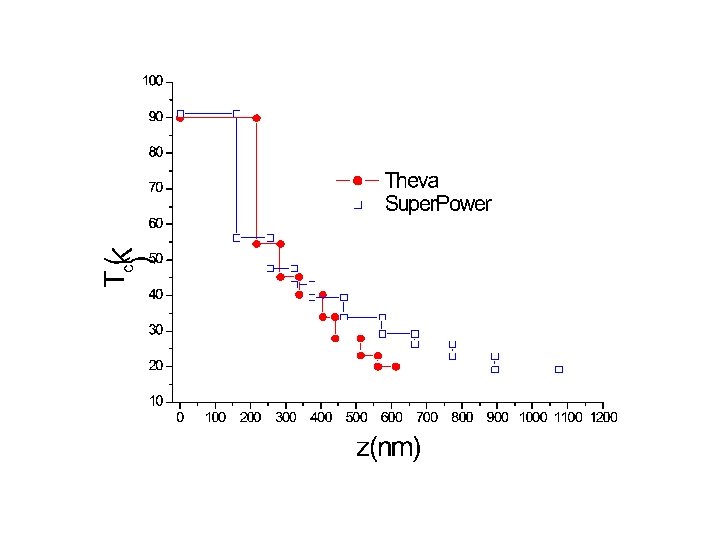
IS THERE A Tc PROFILE ALONG THE THICKNESS OF THE FILMS? { Z { c Z 1 Tc 2 2 Zn { Tcn SUBSTRATE
 EUCAS-Dresden Sept. 2009, Journal of Physics Conference serie")
Transactions on Superconductivity 19, 3541 (2009) EUCAS-Dresden Sept. 2009, Journal of Physics Conference serie 234, 012003 (2010)

YBCO FILMS INCLUDE GENERALLY A LARGE NUMBER OF BOUNDARY PLANES (TWIN BOUNDARIES OR LOW ANGLE GRAIN BOUNDARIES)… JP Contour et al. Thin Solid Films 319, 211 (1998)

…THAT INCLUDE JOSEPHSON WEAK LINKS strains, atomic defects or displacements, vacancies …. xab d 1 d 2 xab : coherence length weak link tunneling current
![…IN Z SUPERIMPOSED ROWS twin boundary c axis Z d [110] Tunneling current P.](http://slidetodoc.com/presentation_image_h2/5d4d5d5a6eab38eef146be3294085382/image-31.jpg "…IN Z SUPERIMPOSED ROWS twin boundary c axis Z d [110] Tunneling current P.")
…IN Z SUPERIMPOSED ROWS twin boundary c axis Z d [110] Tunneling current P. Bernstein, J. F. Hamet and Y. Thimont Physica. C 468, 200 (2008)

CRITICAL SURFACE CURRENT DENSITY: COATED CONDUCTORS if if

WEAK LINKS ROWS WITH DIFFERENT Tc ? c { Z 1 Tc 2 2 Zn c axis { Tcn [110] SUBSTRATE { if if
 Zk dk(nm) 91. 2 80 160 56. 3 47 94 47.")
COATED CONDUCTORS Tck(K) Zk dk(nm) 91. 2 80 160 56. 3 47 94 47. 7 34 68 43. 2 25 50 39. 5 45 90 34 54 108 29. 3 46 92 26. 3 53 106 23 60 120 19. 3 90 181

OXYGEN CONTENT OF A YBCO FILM DEPOSITED ON Sr. Ti. O 3

RESULTS

MICROWAVE ANNEALING of a YBCO/STO FILM

MICROWAVE ANNEALING of a YBCO/STO FILM AT PO 2=500 mbar cumulated microwave energy

MICROWAVE ANNEALING of a YBCO/STO FILM at PO 2=500 mbar d 1 : thickness of the high Tc domain

MICROWAVE ANNEALING: OXYGEN DEPLETION and REDISTRIBUTION in the TWIN and GRAIN BOUNDARIES ? c axis oxygen
 behavior is governed by the")
SUMMARY and CONCLUSIONS 1. The supposition that the JScr(T) behavior is governed by the current flow in the twin and grain boundaries is consistent with the shape of the JScr(T) curve and the existence of a Tc gradient along the c –axis of the films. 2. The superconducting thickness can be different from the deposited thickness and depends probably on the oxygen distribution in the films twin and grain boundaries 3. We have proposed a simple method to determine JScr from T=0 K to Tc 4. The current carried at 77 K depends at first on the width of the high Tc zone in the film.

INVESTIGATION of POWER DISSIPATION MECHANISMS in COATED CONDUCTORS at HIGH CURRENT DENSITIES BASED on ULTRAFAST PULSED CURRENT MEASUREMENTS P. Bernstein, C. Mc. Loughlin, Y. Thimont CRISMAT-ENSICAEN (UMR CNRS 6508) – Caen FRANCE F. Sirois and J. Coulombe Ecole Polytechnique de Montréal - Montréal CANADA

I Rmetal RYBCO METALLIC LAYER : ELECTRICAL SHUNT + HEAT SINK ? INVESTIGATION of the INTRINSIC PHYSICAL PROCESSES OCCURRING within the SUPERCONDUCTING FILMS and the METALLIC LAYERS WHEN an OVERCRITICAL CURRENT FLOWS in CCs

OUTLINE • • PULSED CURRENT MEASUREMENTS THE FLUX FLOW REGIME THE OHMIC REGIME CONCLUSIONS

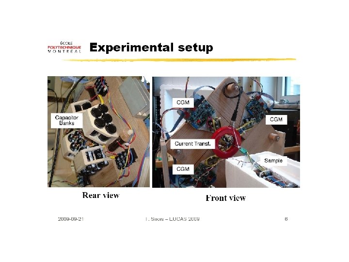
PULSED CURRENT MEASUREMENTS THERMAL EFFECTS OF THE OVERCRITICAL CURRENTS J. Maza et al. Phys. Rev B 78 094512 (2008) 3 -10 ms RISE TIME Currents up to 1000 A (i. e. 10 x Ic) ! « Characterization of electrical resistance of HTS coated conductors at high currents using ultra-fast regulated current pulses » F. Sirois et al. Su. ST 23(3) 034018 (2010)
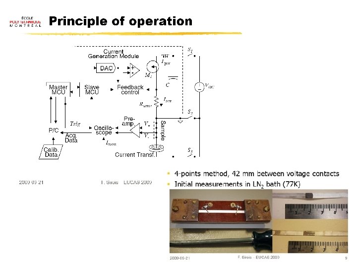

DETERMINATION of the ELECTRIC FIELD at ZERO INJECTED ENERGY

MEASUREMENTS AT 77 K OHMIC FLUX FLOW FLUX CREEP
 ) S 84 10")
CRITICAL and TRANSITION CURRENTS Icr Icff I* (A (A ) ) S 84 10 2 1 9 0 8 S 84 12 2 2 0 3 7

THE FLUX FLOW REGIME
 @77 K Rm")
THE FLUX FLOW REGIME I YBCO Rff metal RS Rs (W) @77 K Rm (W) @77 K S 1 0. 00135 0. 00244 S 2 0. 0136 0. 025

THE FLUX FLOW REGIME: INDUCTIVE VOLTAGE IN THE SHUNT DUE TO THE VORTEX MOTION V’=MV with 0<M<1 I I 1 I 2 + + V Superconducting film - V’ RS metal layer I THE CURRENT IN THE SUPERCONDUCTOR IS A CONSTANT M S 1 S 2 0. 45

THE FLUX FLOW REGIME : THE VORTEX VELOCITY and THE DYNAMIC RESISTANCE Equation of motion Bardeen-Stephen drag coefficient metal film Resistivity rm rn rm instead of rn ! vortex core

THE FLUX FLOW REGIME : THE VORTEX VELOCITY and THE DYNAMIC RESISTANCE Power dissipated in the YBCO film: Moving vortex density P. Bernstein and J. F. Hamet, J. Appl. Phys. 95, 2569 (2004) Vortex velocity : Dynamic resistance :
 Rm")
THE FLUX FLOW REGIME : RESULTS S 1 S 2 v. L (m/s) Rm (W) calculated 2. 26 2. 84 0. 0029 0. 024 Rm (W) P(I*)(W) measured 0. 00244 0. 025 48 687 ( x 0=1. 3 nm )

CONSEQUENCES FOR THE TRANSPORTATION OF POWER AND THE CURRENT LIMITERS Current transport : Rs (and M) small Current limiters : (S 1) ; Rs (and M) large (S 2)

CONCLUSIONS ON THE FLUX FLOW REGIME • ONLY THE NON-DISSIPATIVE CURRENT FLOWS IN THE SUPERCONDUCTOR • THE VORTEX VELOCITY DEPENDS ON THE METAL RESISTIVITY • THE DISSIPATED POWER DEPENDS ON i. e. ON THE METAL LAYER THICKNESS • HOW TO CHANGE M ?

THE OHMIC REGIME FLUX CREEP
 V=R’m. I Rs (W) @77 K I R’m (W) @77")
THE OHMIC REGIME (I>I*) V=R’m. I Rs (W) @77 K I R’m (W) @77 K S 1 0. 00135 0. 00117 Rff RS S 2 0. 0136 0. 0116 R’m<Rs, OK! NO INDUCED VOLTAGE IN THE METAL! BUT Rff-S 1≠Rff-S 2 THE OHMIC REGIME OBSERVED IS APPARENTLY NOT THE NORMAL STATE !

THE OHMIC REGIME : CURRENT IN THE SUPERCONDUCTOR, VORTEX VELOCITY AND DYNAMIC RESISTANCE Power dissipated in the superconductor: Power dissipated in the metal layer: Minimization condition :

VORTEX VELOCITY and CURRENT IN THE SUPERCONDUCTOR
I")
I-Vs IN THE OHMIC REGIME V=R’m(I 1)I

CONCLUSIONS ON THE OHMIC REGIME • THE OHMIC REGIME IS PROBABLY A VORTEX REGIME • THE CURRENT IN THE SUPERCONDUCTOR AND THE VORTEX VELOCITY ARE VERY LOW • THERE IS PROBABLY A PHASE TRANSITION BETWEEN THE FLUX FLOW AND THE OHMIC REGIME

CONCLUSION and PERSPECTIVES 1. 2. 3. THE MAIN RESULT OF THIS WORK IS THAT AN INDUCTIVE VOLTAGE IS GENERATED IN THE METAL BY THE MOTION OF THE VORTICES IN THE SUPERCONDUCTOR. HOWEVER WE KNOW LITTLE ON THE COUPLING MECHANISMS AND THE FACTORS ACTING ON M, WHILE THIS QUANTITY AS WELL AS THE METAL THICKNESS CAN BE ESSENTIAL TOOLS TO CUSTOMIZE THE COATED CONDUCTORS FOR A GIVEN APPLICATION. THE VORTEX REGIME IN THE OHMIC REGIME IS NOT CLEAR AND SHOULD BE INVESTIGATED. THE EFFECT OF THE INITIAL STEPS OF THE TRANSITION TO THE NORMAL STATE OF THE COATED CONDUCTORS ON THE OVERALL PROCESS IS NOT YET WELL ESTABLISHED


CONCLUSIONS FLUX FLOW REGIME : • ONLY the NON-DISSIPATIVE CURRENT FLOWS in YBCO • An INDUCTIVE VOLTAGE is GENERATED in the METAL FILM by THE VORTEX MOTION in the SUPERCONDUCTING LAYER • The VORTEX VELOCITY DEPENDS on the RESISTIVITY of the METALLIC SHUNT • THE OHMIC REGIME does not CORRESPOND to the NORMAL STATE RATHER a VORTEX REGIME • THERE is PROBABLY a FIRST ORDER TRANSITION BETWEEN THE FLUX FLOW and the OHMIC REGIME • The POWER DISSIPATION in the CCs at HIGH CURRENTS is DETERMINED PRIMARILY by the METAL LAYER RESISTANCE and the COUPLING FACTOR M

THE OHMIC REGIME : THE CURRENT IN THE SUPERCONDUCTOR Power dissipated in the superconductor: Power dissipated in the metal layer: Minimization condition : Resistance in the ohmic regime :

THE OHMIC REGIME : CURRENT IN THE SUPERCONDUCTOR, VORTEX VELOCITY AND DYNAMIC RESISTANCE Power dissipated in the superconductor: Power dissipated in the metal layer: Minimization condition : Resistance in the ohmic regime :


CRITICAL SURFACE CURRENT DENSITY: YBCO FILMS ON SINGLE CRYSTALS T>0. 4 -0. 5 Tc d 0=0. 55 nm P. Bernstein, J. F. Hamet and Y. Thimont, Physica. C 468, 200 (2008) see also : P. Bernstein, J. F. Hamet and Y. Thimont, IEEE Trans. Appl. Supercond. 19, 3541 (2009)

SUPERCONDUCTING vs DEPOSITED THICKNESS


CRITICAL CURRENT DENSITY AT 77 K OF COATED CONDUCTORS
")
YBCO/STO : Oxygen Content Profile Obtained from Non Rutherford Elastic Resonance Scattering Spectra (NRES) [J. Siejka, INSP (Paris)] phase transition d (nm) 110 ds (nm) 85 “Measurements of the surface critical current of YBa 2 Cu 3 O 7 thin films : probing the non-uniformity of their superconducting critical temperature along the c-axis”, P. Bernstein, J. Mosqueira, J. Siejka, F. Vidal, Y. Thimont, C. Mc. Loughlin and G. Ferro, to be published in the Journal of Applied Physics

MICROWAVE ANNEALING of a YBCO/STO FILM at PO 2=500 mbar d 1 : thickness of the high Tc domain
 Kim et al. Supercond. Sc.")
Foltyn et al. Appl. Phys. Lett. 75, 3692 (1999) Kim et al. Supercond. Sc. Techn. 19, 968 (2006)

MICROWAVE ANNEALING AT PO 2=500 mbar of a YBCO/STO FILM

RESULTS
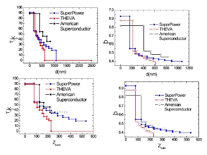

CONCLUSIONS 1. 2. 3. 4. The Tc and oxygen profiles in CC can be very different from one sample to the other one. The possible decrease of jcr with the YBCO film thickness can probably be ascribed to a low oxygen content of some buried areas in the film. The mean height of the weak links rows depends on the investigated CC, while we find always almost the same value for YBCO/STO The current carried at 77 K depends at first on the width of the high Tc zone in the film.

CONCLUSIONS 1. 2. 3. 4. The Tc and oxygen profiles in CC can be very different from one sample to the other one. The possible decrease of jcr with the YBCO film thickness can probably be ascribed to a low oxygen content of some buried areas in the film. The mean height of the weak links rows depends on the investigated CC, while we find always almost the same value for YBCO/STO The current carried at 77 K depends at first on the width of the high Tc zone in the film.

c Z 1 Z 2 { { Zn { c axis { Z 1 2 [110] SAMPLE Am. Super. 3. 2 Super. P 2 Theva 2. 7 YBCO/STO 1. 4 c h

CONCLUSIONS 1. 2. 3. 4. The Tc and oxygen profiles in CC can be very different from one sample to the other one. The possible decrease of jcr with the YBCO film thickness can probably be ascribed to a low oxygen content of some buried areas in the film. The mean height of the weak links rows depends on the investigated CC, while we find always almost the same value for YBCO/STO The current carried at 77 K depends at first on the width of the high Tc zone in the film.

TRANSITION A L’ETAT NORMAL P. Bernstein, J. F. Hamet, M. T. Gonzalez , M. Ruibal Acuna, Physica. C 455(2007)1– 12


YBCO on Single Crystal


ds

WEAK LINKS ROWS WITH DIFFERENT Tc ? c axis Tc 1 Tc 2 Tc 3 Tc 4 { Z 1 Z 2 Z 3 Z 4 [110] if if

LEY 9275 3 ö 2 Tc 2 pk B T æç T ÷ J Scr = Z 1 f o d o çè 2 Tc ÷ø Tc S = S æ Tc ö < ÷ T J cr ç 2 è 2 ø T< = I cr w Z=7 Tc=87. 8 K
![Oxygen depletion in the grain boundaries and twin boundaries c axis [110] oxygen](http://slidetodoc.com/presentation_image_h2/5d4d5d5a6eab38eef146be3294085382/image-102.jpg "Oxygen depletion in the grain boundaries and twin boundaries c axis [110] oxygen")
Oxygen depletion in the grain boundaries and twin boundaries c axis [110] oxygen

ION MILLING : OXYGEN DEPLETION IN THE TWIN AND GRAIN BOUNDARIES DUE TO THE ION BOMBARDMENT ? c axis oxygen

YBCO/Sr. Ti. O 3

PHYSICAL THICKNESS and SUPERCONDUCTING THICKNESS DATA ON THE LINE: ds dph
")
SURFACE CRITICAL CURRENT DENSITY AT LOW TEMPERATURE (Tmin)

SURFACE CRITICAL CURRENT DENSITY
 SAMPLE dph (nm) ds(nm) American 1 mm Superconductor 0.")
1 - SUPERCONDUCTING THICKNESS (ds) SAMPLE dph (nm) ds(nm) American 1 mm Superconductor 0. 8 mm* Theva 2. 5 mm 0. 6 mm Super. Power 1 mm * underestimated

RESULTS

SUMMARY and CONCLUSIONS -1 • We have proposed a simple method to determine JScr from T=0 K to Tc • Films deposited on single crystals and coated conductors show similar properties, although jcr(Tmin) is larger in the case of the films deposited on single crystals • The shape of the JScr(T) curve is consistent with a Tc gradient along the c –axis of the films • The current carried at 77 K depends at first on the width of the high Tc zone in the film.

PHYSICAL THICKNESS and SUPERCONDUCTING THICKNESS DATA ON THE LINE: ds dph
 [J.")
YBCO/STO : Tc PROFILE OBTAINED FROM Non Rutherford Elastic Resonance Scattering Spectra (NRES) [J. Siejka, INSP (Paris)] J. D. Jorgensen et al. Phys. Rev. B 41, 1863 (1990) “Measurements of the surface critical current of YBa 2 Cu 3 O 7 -d thin films : probing the non-uniformity of their superconducting critical temperature along the c-axis” P. Bernstein et al. to be published in the Journal of Applied Physics

Non Superconducting Area YBCO/Sr. Ti. O 3
 ds dd (nm) Tck (K) Zk dk (nm)")
YBCO/Sr. Ti. O 3 (LEY 9275) ds dd (nm) Tck (K) Zk dk (nm) 233 87. 5 17 24. 5 82. 5 11 15. 8 61. 5 10 14. 4 48. 5 17 24. 5 39. 5 18 25. 9 33. 7 13 18. 7 Measurements by J. Mosqueira and F. Vidal - LBTS Santiago de Compostela P. Bernstein et al. to be published in J. Appl. Phys.

3 –OXYGEN DISTRIBUTION ?

MICROWAVE ANNEALING of a YBCO/STO FILM AT PO 2=500 mbar

MICROWAVE ANNEALING of a YBCO/STO FILM AT PO 2=500 mbar d 1 : thickness of the high Tc domain

MICROWAVE ANNEALING of a YBCO/STO FILM AT PO 2=500 mbar
- Slides: 118