LED Photolithography Dicing LED Etching Metallization LappingPolishing Dicing

 * 에피탁시 (Epitaxy) : 결정방위가 유사한 분자구조를 기판 위에 화학적(MOCVD) 또는 물리")
 1. 전극/절연막 증착 LED 구조 4. Oxide etching (RIE) Si.")
 6. PR coating 8. Metallization 기판 7. 노광 (photolithography) 기판")
 투명전극 (금속박막 또는 금속산화물) (+) (-) p-Ga. N (0. 2")
 (+) Window (p-Ga. P) Upper confining layer Active")
- Slides: 7
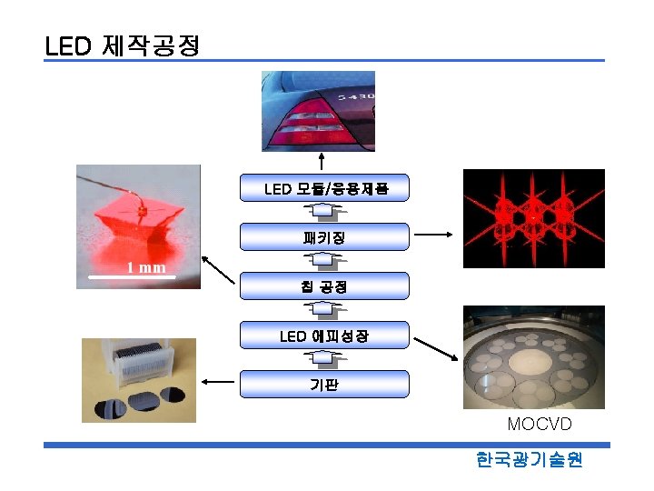
LED 칩 공정 Photolithography Dicing 된 LED 칩 Etching Metallization Lapping/Polishing Dicing 0. 3 mm 한국광기술원
에피성장 (Epitaxy) * 에피탁시 (Epitaxy) : 결정방위가 유사한 분자구조를 기판 위에 화학적(MOCVD) 또는 물리 적(MBE) 방법으로 p-n 접합층을 형성. on (epi) + arrangement (taxy) (CH 3)3 Ga (CH 3)3 In n형 dopant (Si 2 H 6) NH 3 p형 dopant (Cp 2 Mg) p-Ga. N QW In. Ga. N n-Ga. N 기판 기판 ~ 1080 o. C (CH 3)3 Ga + NH 3 MO gas = Ga. N + 3 CH 4 (byproduct) MOCVD 방법에 의한 박막성장
칩 제작공정 (Nitride LED) 1. 전극/절연막 증착 LED 구조 4. Oxide etching (RIE) Si. O 2 (절연막) Metal(투명전극) LED 구조 기판 기판 5. PR 제거 후 Ga. N etching (ICP) 2. 노광 (photolithography) Mask PR LED 구조 기판 기판 3. Development 절연막 제거후 RTA LED 구조 기판 기판
칩 제작공정 (Nitride LED) 6. PR coating 8. Metallization 기판 7. 노광 (photolithography) 기판 9. Lift-off 기판 기판 10. Lapping/Polishing 기판 기판 11. Scribing/Breaking
LED 칩 (Nitride LED) 투명전극 (금속박막 또는 금속산화물) (+) (-) p-Ga. N (0. 2 um) QW’s n-Ga. N (3 um) Ga. N buffer Sapphire Chip dimension = 0. 3 x 0. 1 mm 3 P
LED 칩 (Al. Ga. In. P) (+) Window (p-Ga. P) Upper confining layer Active layer Lower confining layer Al. Ga. In. P MQW Al. As/Al. Ga. As DBR Wafer bonding Substrate (n-Ga. As) (-) Substrate (n-Ga. P) (-)