LED continued LED LED CHUNGBUK TECHNOPARK REGIONAL EVALUATION

LED는 어떻게 생겼나? continued 위에서 본 LED 사진 옆에서 본 LED 사 진 자료 : CHUNGBUK TECHNOPARK REGIONAL EVALUATION AGENCY 1
 자료 : LG Innotek LED overview 2")
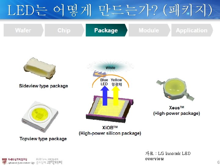
LED는 어떻게 만드는가? (전체) 자료 : LG Innotek LED overview 2
 자료 : LG Innotek LED overview 3")
LED는 어떻게 만드는가? (에피) 자료 : LG Innotek LED overview 3
 Chip pattern photo mask 자료 : LG Innotek LED overview")
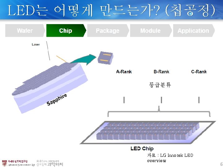
LED는 어떻게 만드는가? (칩공정) Chip pattern photo mask 자료 : LG Innotek LED overview 4

q 고출력 LED 구현 시 문제점 – efficiency droop v 고효율 Ga. N LED의 문제점 Origin of the efficiency droop Cause Description Possible solution Auger loss • Auger recombination (electron-electron scattering) • High current density in active region DH structure Crystal defect • High defect density of Ga. N • Electron tunneling between threading dislocations • Non-radiative emission • In localization ↑ • Defect reduction in Ga. N sub. Polarization field • Carrier delocalization from localized states • Polarization reduction (Quaternary) • Non-polar Carrier leakage • Electron leakage through electron-blocking layer (EBL layer) • Lack of hole injection • Electrons recombine with holes outside the active region. Polarization reduction (polarization-matched active region) • Need for In. Ga. N/Ga. N MQW optimization and p-Al. Ga. In. N/Ga. N superlattices (SLs) - p-Al. Ga. N EBL을 p-Al. Ga. In. N/Ga. N SLs 구조로 대체 - electron leakage ↓ & hole injection ↑ Ref : Research of RPI - Radiative recombination ↑ Advance semiconductor lab

q Epi 설계를 통한 구조 최적화 예- EBL v Al. Ga. In. N/Ga. N super-lattices (SLs) 구조를 이용한 고효율 Ga. N LED 에피구조 설계 Ti/Al/Ni/Au 1. p-Al 0. 15 Ga. N EBL 2. p-Al 0. 38 Ga 0. 46 In 0. 16 N EBL 3. p-Al 0. 38 Ga 0. 46 In 0. 16 N/Ga. N SLs 100 nm ITO 200 nm p-Ga. N 40 nm EBL 5 period In. Ga. N(3 nm)/Ga. N(12 nm)MQW Ni/Au 2. 5μm n-Ga. N Sapphire sub. 28. 6 % 증가 § Si. LENSe and Spe. CLED to investigate the performance of the Ga. N-based LEDs § The material parameters of Inx. Ga. N 1 -x, Alx. Ga 1 -x, and Alx. Ga 1 -x-y. Iny. N are autometically calculated by linear interpolation as a function of composition fraction (x) and (y) in Si. LENSe software § Size : 500 μm X 500 μm 28. 7 % 증가 Al. Ga. In. N/Ga. N SLs EBL를 적용한 구조에 서 efficiency droop 현상의 감소가 나타남 (@ Injection current 150 m. A) Advance semiconductor lab
 p-Al. Ga. In.")
q Epi 구조 최적화 예- EBL v p-Al. Ga. N, (b) p-Al. Ga. In. N, (c) p-Al. Ga. In. N/Ga. N SLs 장벽층 구조에 따른 전자 및 정공의 분포 hole electron 장벽층의 구조에 따른 전자 및 정공의 농도 (@ Injection current 20 m. A) § p-Al. Ga. In. N/Ga. N SLs EBL 구 조 의 3, 4, 5 번 째 quantum well내의 전자 및 정공의 농도가 p-Al. Ga. N 및 p-Al. Ga. In. N EBL 구조보다 높음 5번째 quantum well에서 - electron leakage를 억제 - 효율적인 hole injection 발광 재결합 향상 광출력 및 EQE 증가 Advance semiconductor lab
 개발 목표 (")
q 칩기술: 광 추출효율 향상의 중요성 미국 NGLI(Next Generation Lighting Initiative) 개발 목표 ( 단위: %) LED 구현시 문제점 및 원인 LED 광소자 (pkg 단위) 내부양자 광추출 전기주입 형광체/산란 광학부품, 등기구 85 60 50 70 75 70 8 90+ 95 90 90 85 90 50 년도 Driver 2007 2015 총 효율 LED Chip에서의 광추출효율 저하문제 발생! LED-Optical Properties-Light Escape Cone • The angle of total internal reflection defines the light escape cone. sinθc = nair/ns, θc=23° • Area of the escape cone = 2πr 2(1 -cosθc) • Pescape / Psource = (1 -cosθc)/2 = θc 2/4 = (nair 2/ns 2)/4 ~ 4% (ns=2. 46 for Ga. N) LED의 광추출효율 향상을 위한 Chip 공정기술 개발 必要

q 광 추출효율 향상기술 v 광추출효율 향상 방안 § Nano-imprinting lithography § Laser holography § Electron-beam lithography § Nanosphere lithography(NSL) Photonic crystal § Photons are localized into discrete energy states § Energy range with no permitted states forms: known as a photonic band gap § Properties of the bandgap dependent upon several engineering ingredients

q LED 칩 효율: lateral LED vs. vertical LED 광추출효율-ray optics model LED on Sapphire QW Photon outside QW QW Sapphire 기판 32. 8 % 수직형 칩(R 90%, roughened surface) 수직형 칩 R 90% 반사막 Receptor 기판 24. 6% (반사율 60%) 56. 2 % (반사율 90%) Receptor 기판 69. 8 % (w/ micro rougheness) 73. 5 % (w/ nano rougheness) 한국광기술원
- Slides: 13