Lecture2 Basics of Semiconductor Physics 3 rd International
Lecture-2: Basics of Semiconductor Physics 3 rd International Workshop on Tracking Detectors in High Energy Physics October 19 -21, 2020 National Centre for Physics, Islamabad-Pakistan Saif Ullah Awan, Ph. D Associate Professor Department of Electrical Engineering National University of Sciences and Technology (NUST) Islamabad, Pakistan Emails: saifullahawan@ceme. nust. edu. pk ullahphy@gmail. com 1

2
Acknowledgements 1. Semiconductor detectors by Silvia Masciocchi, GSI Darmstadt and University of Heidelberg 39 th Heidelberg Physics Graduate Days, HGSFP Heidelberg 2. Indian Institute of Technology Hans-Jürgen Wollersheim 3. Gerhard Lutz, Semiconductor, Radiation Detectors Device Physics 4. hyperphysics. phy 3
Layout of talk • Crystal structure • Bond model and Band model for Semiconductors • Conduction in Semiconductors Lecture-2 • N-Type and P-Type Semiconductors • The Diode (pn Junction) • Biasing a Diode • Silicon Wafer Production • Production of metallurgical grade (MG)-Si • Electronic Grade Polycrystalline Silicon (Polysilicon) Purification 4
Example of N-type And P-type Semiconductors is Diode 5
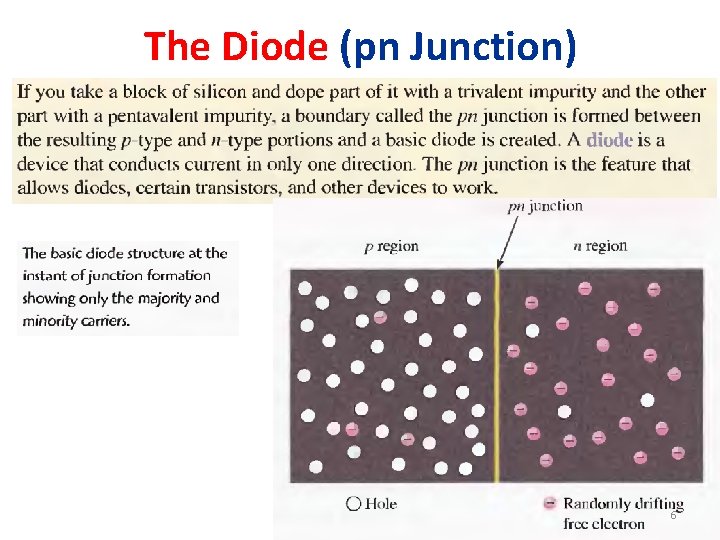
The Diode (pn Junction) 6
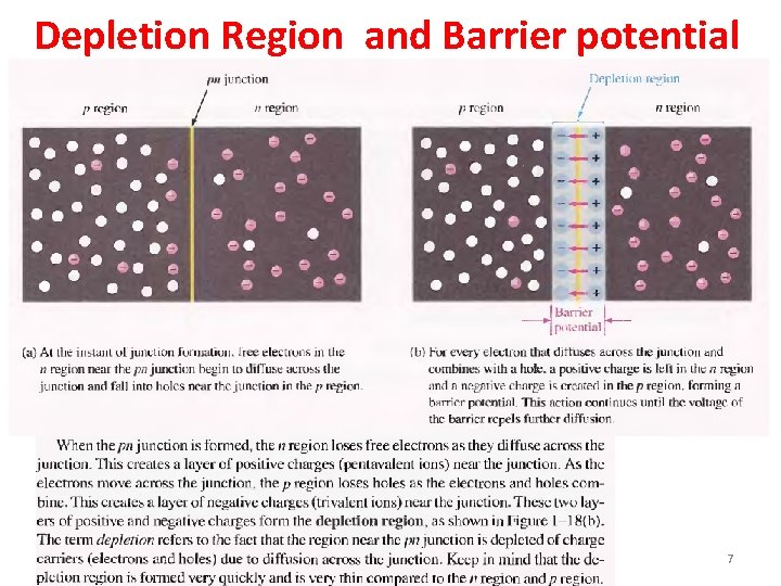
Depletion Region and Barrier potential 7
8

9

10
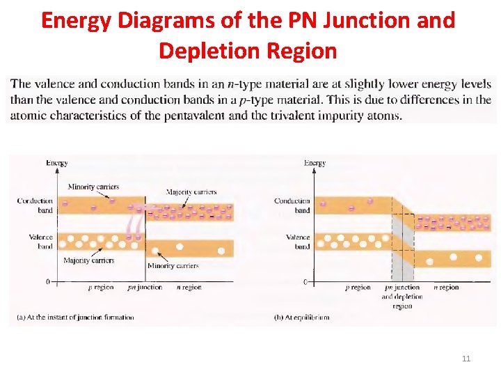
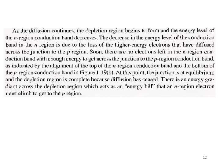
Energy Diagrams of the PN Junction and Depletion Region 11
12
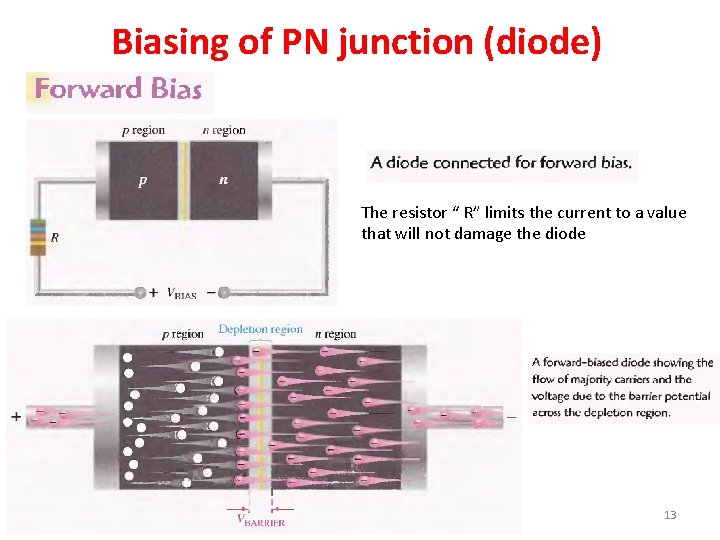
Biasing of PN junction (diode) The resistor “ R” limits the current to a value that will not damage the diode 13
14
15
16
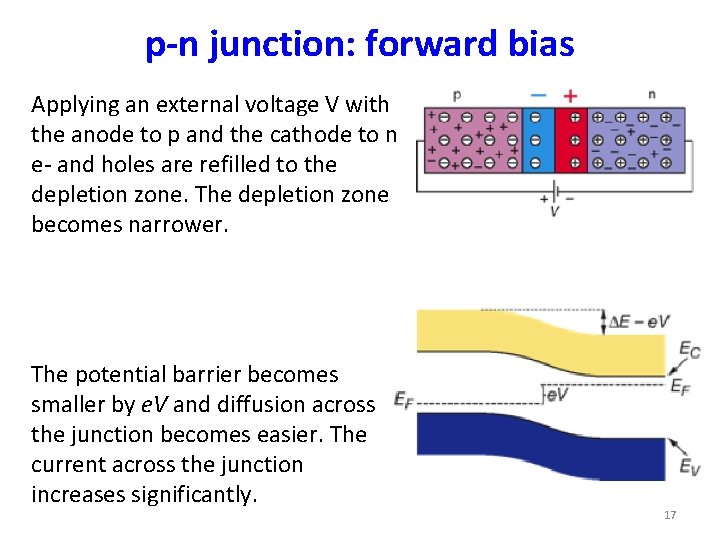
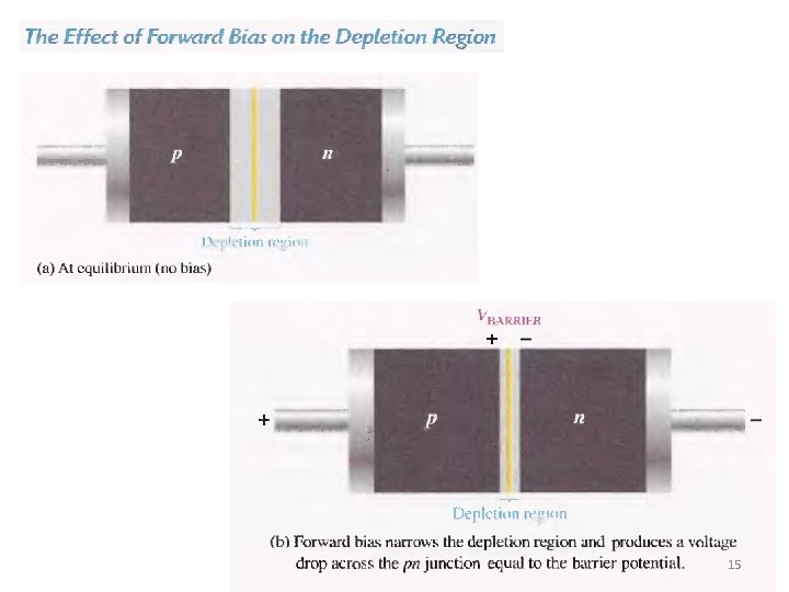
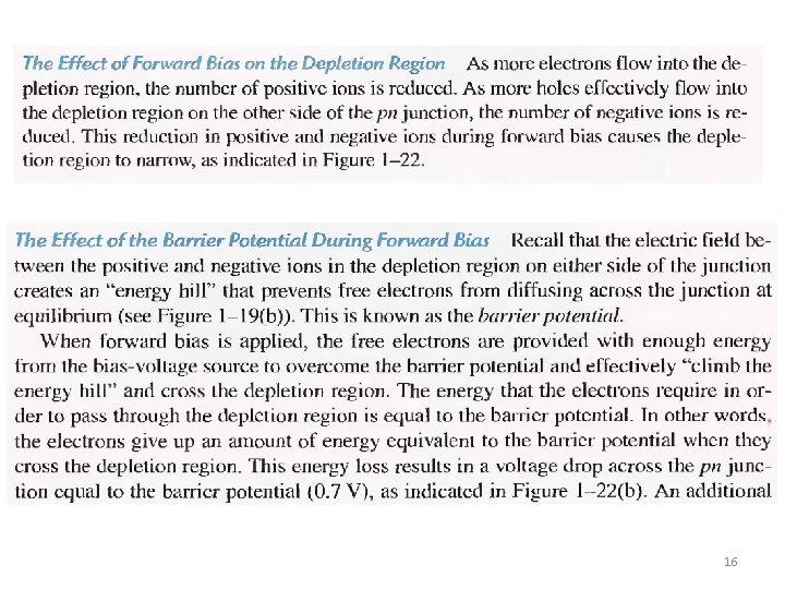
p-n junction: forward bias Applying an external voltage V with the anode to p and the cathode to n e- and holes are refilled to the depletion zone. The depletion zone becomes narrower. The potential barrier becomes smaller by e. V and diffusion across the junction becomes easier. The current across the junction increases significantly. 17
18
19
20
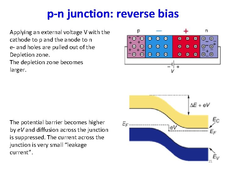
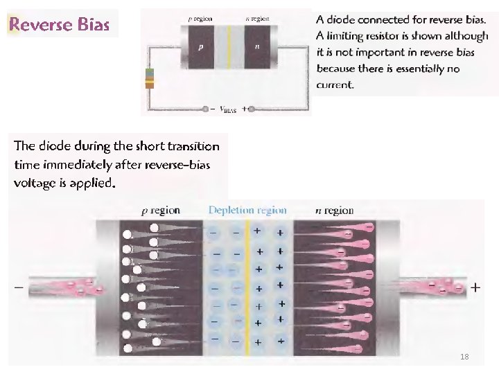
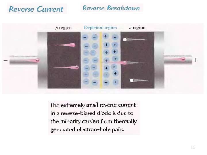
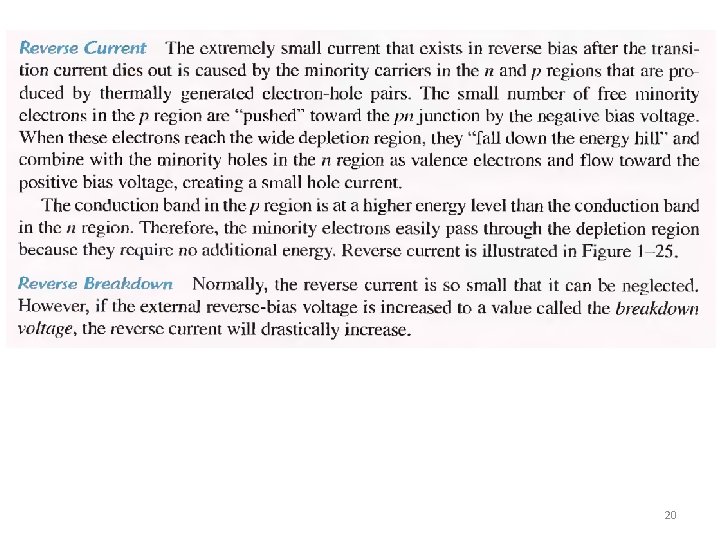
p-n junction: reverse bias Applying an external voltage V with the cathode to p and the anode to n e- and holes are pulled out of the Depletion zone. The depletion zone becomes larger. The potential barrier becomes higher by e. V and diffusion across the junction is suppressed. The current across the junction is very small “leakage current”. 21
Manufacture of single crystal silicon Introduction: • The synthesis and purification of bulk polycrystalline semiconductor material represents the first step towards the commercial fabrication of an electronic device. • This polycrystalline material is then used as the raw material for the formation of single crystal material that is processed to semiconductor wafers. • The strong influence on the electric characteristics of a semiconductors exhibited by small amounts of some impurities requires that the bulk raw material be of very high purity (> 99. 9999%). • Although some level of purification is possible during the crystallization process it is important to use as high a purity starting material as possible 22
Manufacture of single crystal silicon Introduction: • Following oxygen (46%), silicon (L. silicis flint) is the most abundant element in the earth's crust (28%). • However, silicon does not occur in its elemental form, but as its oxide (Si. O 2) or as silicates. Sand, quartz, amethyst, agate, flint, and opal are some of the forms in which the oxide appears. • Granite, hornblende, asbestos, feldspar, clay and mica, etc. are a few of the numerous silicate minerals. • With such boundless supplies of the raw material, the costs associated with the production of bulk silicon is not one of abstraction and conversion of the oxide(s), but of purification of the crude elemental silicon. • While 98% elemental silicon, known as metallurgical-grade silicon (MGS), is readily produced on a large scale, the requirements of extreme purity for electronic device fabrication require additional purification steps in order to produce electronic-grade silicon (EGS). Electronic-grade silicon is also known as semiconductor-grade silicon (SGS). • In order for the purity levels to be acceptable for subsequent crystal growth and device fabrication, EGS must have carbon and oxygen impurity levels less than a few parts per million (ppm), and metal 23 impurities at the parts per billion (ppb) range or lower.
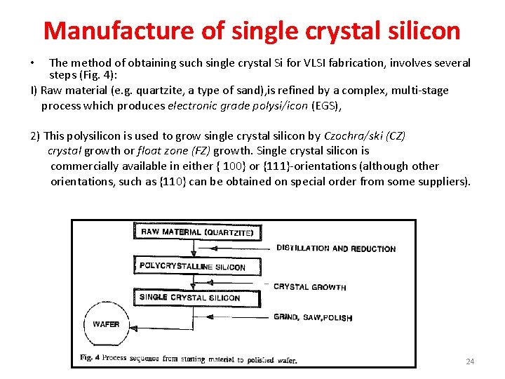
Manufacture of single crystal silicon The method of obtaining such single crystal Si for VLSI fabrication, involves several steps (Fig. 4): I) Raw material (e. g. quartzite, a type of sand), is refined by a complex, multi-stage process which produces electronic grade polysi/icon (EGS), • 2) This polysilicon is used to grow single crystal silicon by Czochra/ski (CZ) crystal growth or float zone (FZ) growth. Single crystal silicon is commercially available in either { 100} or {111}-orientations (although other orientations, such as {110} can be obtained on special order from some suppliers). 24
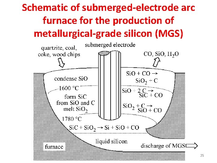
Schematic of submerged-electrode arc furnace for the production of metallurgical-grade silicon (MGS) 25
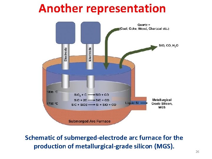
Another representation Schematic of submerged-electrode arc furnace for the production of metallurgical-grade silicon (MGS). 26
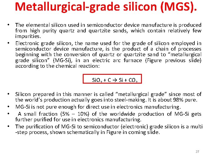
Metallurgical-grade silicon (MGS). • The elemental silicon used in semiconductor device manufacture is produced from high purity quartz and quartzite sands, which contain relatively few impurities. • Electronic grade silicon, the name used for the grade of silicon employed in semiconductor device manufacture, is the product of a chain of processes beginning with the conversion of quartz or quartzite sand to “metallurgical grade silicon” (MG-Si), in an electric arc furnace (Figure previous slide) according to the chemical reaction: Si. O 2 + C → Si + CO 2 • Silicon prepared in this manner is called “metallurgical grade” since most of the world’s production actually goes into steel-making. It is about 98% pure. • MG-Si is not pure enough for direct use in electronics manufacturing. • A small fraction (5% – 10%) of the worldwide production of MG-Si gets further purified for use in electronics manufacturing. • The purification of MG-Si to semiconductor (electronic) grade silicon is a multi -step process, shown schematically in Figure in coming slide. 27
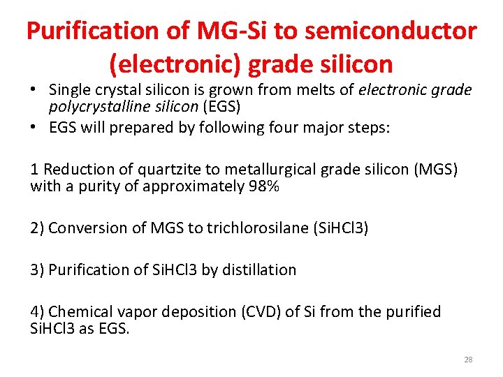
Purification of MG-Si to semiconductor (electronic) grade silicon • Single crystal silicon is grown from melts of electronic grade polycrystalline silicon (EGS) • EGS will prepared by following four major steps: 1 Reduction of quartzite to metallurgical grade silicon (MGS) with a purity of approximately 98% 2) Conversion of MGS to trichlorosilane (Si. HCl 3) 3) Purification of Si. HCl 3 by distillation 4) Chemical vapor deposition (CVD) of Si from the purified Si. HCl 3 as EGS. 28
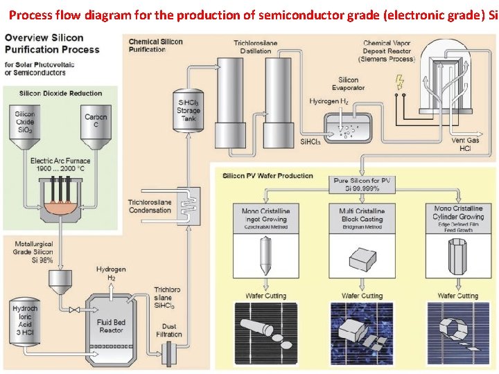
Process flow diagram for the production of semiconductor grade (electronic grade) Si 29
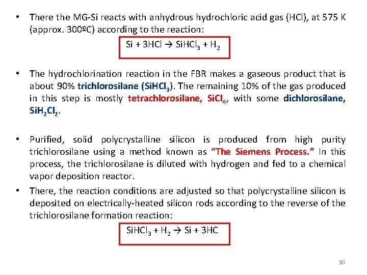
• There the MG-Si reacts with anhydrous hydrochloric acid gas (HCl), at 575 K (approx. 300ºC) according to the reaction: Si + 3 HCl → Si. HCl 3 + H 2 • The hydrochlorination reaction in the FBR makes a gaseous product that is about 90% trichlorosilane (Si. HCl 3). The remaining 10% of the gas produced in this step is mostly tetrachlorosilane, Si. Cl 4, with some dichlorosilane, Si. H 2 Cl 2. • Purified, solid polycrystalline silicon is produced from high purity trichlorosilane using a method known as “The Siemens Process. ” In this process, the trichlorosilane is diluted with hydrogen and fed to a chemical vapor deposition reactor. • There, the reaction conditions are adjusted so that polycrystalline silicon is deposited on electrically-heated silicon rods according to the reverse of the trichlorosilane formation reaction: Si. HCl 3 + H 2 → Si + 3 HC 30
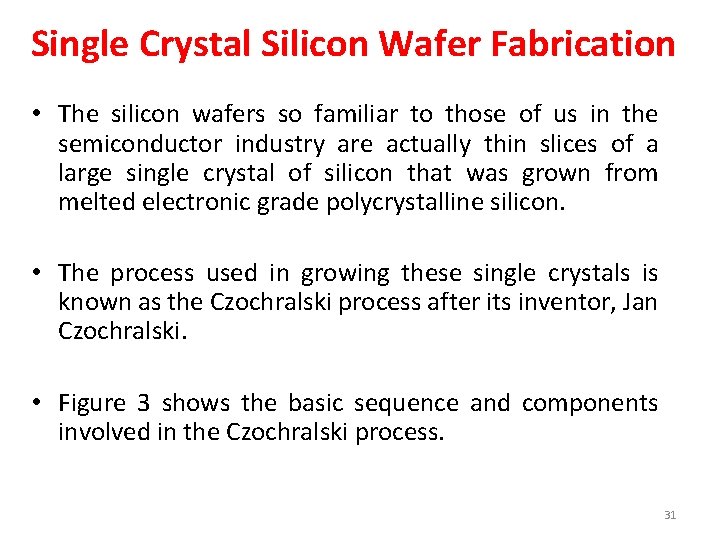
Single Crystal Silicon Wafer Fabrication • The silicon wafers so familiar to those of us in the semiconductor industry are actually thin slices of a large single crystal of silicon that was grown from melted electronic grade polycrystalline silicon. • The process used in growing these single crystals is known as the Czochralski process after its inventor, Jan Czochralski. • Figure 3 shows the basic sequence and components involved in the Czochralski process. 31
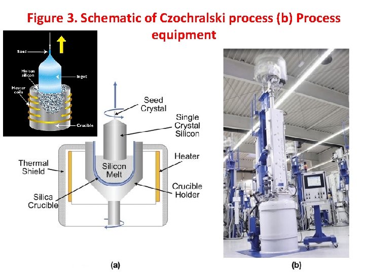
Figure 3. Schematic of Czochralski process (b) Process equipment 32
Czochralski process • • • The Czochralski process is carried out in an evacuable chamber, commonly referred to as a “crystal puller” that holds a large crucible, usually quartz, and an electric heating element (Figure 3(a)). Semiconductor grade polysilicon is loaded (charged) into the crucible along with precise amounts of any dopants such as phosphorus or boron that may be needed to give the product wafers specified P or N characteristics. Evacuation removes any air from the chamber to avoid oxidation of the heated silicon during the growth process. The charged crucible is electrically heated to a temperature sufficient to melt the polysilicon (greater than 1421ºC). Once the silicon charge is fully melted, a small seed crystal, mounted on a rod, is lowered into the molten silicon. The seed crystal is typically about 5 mm in diameter and up to 300 mm long. It acts as a “starter” for the growth of the larger silicon crystal from the melt. The seed crystal is mounted on the rod with a known crystal facet vertically oriented in the melt (crystal facets are defined by “Miller Indices”). In the case of seed crystals, facets having Miller indices of <100>, <110> or <111> are typically chosen. The crystal growth from the melt will conform to this initial orientation, giving the final large single crystal a known crystal orientation. Following immersion in the melt, the seed crystal is slowly (a few cm/hour) pulled from the melt as the larger crystal grows. The pull speed determines the final diameter of the large crystal. Both the crystal and the crucible are rotated during a crystal pull to improve the homogeneity of the crystal and dopant distribution. The final large crystal is cylindrical in shape; it is called a “boule. ” Czochralski growth is the most economical method for the production of silicon crystal boules suitable for producing silicon wafers for general semiconductor device fabrication (known as CZ wafers). The method can form boules large enough to produce silicon wafers up to 450 mm in diameter. 33
Limitations of Czochralski process • However, the method has certain limitations. Since the boule is grown in a quartz (Si. O 2) crucible, some oxygen contamination is always present in the silicon (typically 1018 atoms cm-3 or 20 ppm). Graphite crucibles have been used to avoid this contamination, however they produce carbon impurities in the silicon, albeit at an order of magnitude lower in concentration. Both oxygen and carbon impurities lower the minority carrier diffusion length in the final silicon wafer. Dopant homogeneity in the axial and radial directions is also limited in Czochralski silicon, making it difficult to obtain wafers with resistivities greater than 100 ohm-cm. 34
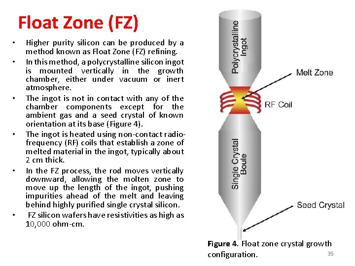
Float Zone (FZ) • • • Higher purity silicon can be produced by a method known as Float Zone (FZ) refining. In this method, a polycrystalline silicon ingot is mounted vertically in the growth chamber, either under vacuum or inert atmosphere. The ingot is not in contact with any of the chamber components except for the ambient gas and a seed crystal of known orientation at its base (Figure 4). The ingot is heated using non-contact radiofrequency (RF) coils that establish a zone of melted material in the ingot, typically about 2 cm thick. In the FZ process, the rod moves vertically downward, allowing the molten zone to move up the length of the ingot, pushing impurities ahead of the melt and leaving behind highly purified single crystal silicon. FZ silicon wafers have resistivities as high as 10, 000 ohm-cm. Figure 4. Float zone crystal growth 35 configuration.
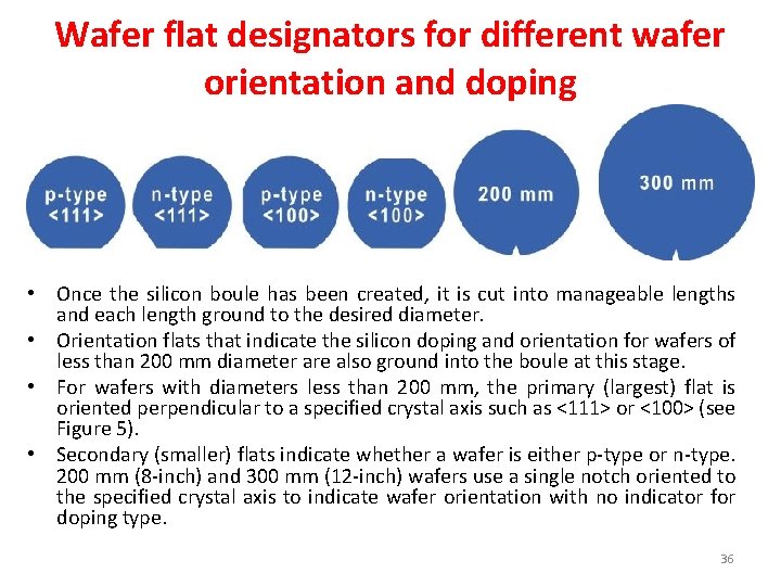
Wafer flat designators for different wafer orientation and doping • Once the silicon boule has been created, it is cut into manageable lengths and each length ground to the desired diameter. • Orientation flats that indicate the silicon doping and orientation for wafers of less than 200 mm diameter are also ground into the boule at this stage. • For wafers with diameters less than 200 mm, the primary (largest) flat is oriented perpendicular to a specified crystal axis such as <111> or <100> (see Figure 5). • Secondary (smaller) flats indicate whether a wafer is either p-type or n-type. 200 mm (8 -inch) and 300 mm (12 -inch) wafers use a single notch oriented to the specified crystal axis to indicate wafer orientation with no indicator for doping type. 36

37
- Slides: 37