Lecture1 Basics of Semiconductor Physics 3 rd International

Lecture-1: Basics of Semiconductor Physics 3 rd International Workshop on Tracking Detectors in High Energy Physics October 19 -21, 2020 National Centre for Physics, Islamabad-Pakistan Saif Ullah Awan, Ph. D Associate Professor Department of Electrical Engineering National University of Sciences and Technology (NUST) Islamabad, Pakistan Emails: saifullahawan@ceme. nust. edu. pk ullahphy@gmail. com


Acknowledgements 1. Semiconductor detectors by Silvia Masciocchi, GSI Darmstadt and University of Heidelberg 39 th Heidelberg Physics Graduate Days, HGSFP Heidelberg 2. Indian Institute of Technology Hans-Jürgen Wollersheim 3. Gerhard Lutz, Semiconductor, Radiation Detectors Device Physics 4. hyperphysics. phy

Layout of talk • Crystal structure • Bond model and Band model for Semiconductors • Conduction in Semiconductors • N-Type and P-Type Semiconductors • The Diode (pn Junction) • Biasing a Diode • PNP transitor

Introduction of Crystalline and non-crystalline

Atoms in a Crystal Is this is ideal or real Crystal ?
mono (or) single crystals (b) polycrystalline solids (c) amorphous solids")
ATOMIC ARRANGEMENT IN CRYSTALS (a)mono (or) single crystals (b) polycrystalline solids (c) amorphous solids 7


Bravais Lattices 3 -Dimentional 10

Diamond like Crystal structure of Si Silicon crystallizes in the same pattern as diamond, in a structure which Ashcroft and Mermin call "two interpenetrating face-centered cubic" primitive lattices.
 of Si • Atoms touch each other along face")
Face Centered Cubic Structure (FCC) of Si • Atoms touch each other along face diagonals. --Note: All atoms are identical; the face-centered atoms are shaded differently only for ease of viewing. ex: Al, Cu, Au, Pb, Ni, Pt, Ag 4 atoms/unit cell: (6 face x ½) + (8 corners x 1/8)

Atomic Structure of Si

Band structure of electron levels Solid → crystalline structure of atoms in a lattice, with covalent bonds. The periodic arrangement of atoms in the crystal causes an overlap of electron wave-functions, which creates a “band” of energy states allowed for the outermost shell energy levels. Electrons are fermions: the Pauli principle forbids to have more than one electron in the same identical state and this produces a degeneracy in the outer atomic shell energy levels. This produces many discrete levels which are very close to each other, which appear as “bands” The innermost energy levels are not modified, and the electrons remain associated to the respective lattice atoms. CONDUCTION BAND: electrons are detached from parent atoms and are free to move about the whole crystal VALENCE BAND: electrons are more tightly bound and remain associated to the respective lattice atom
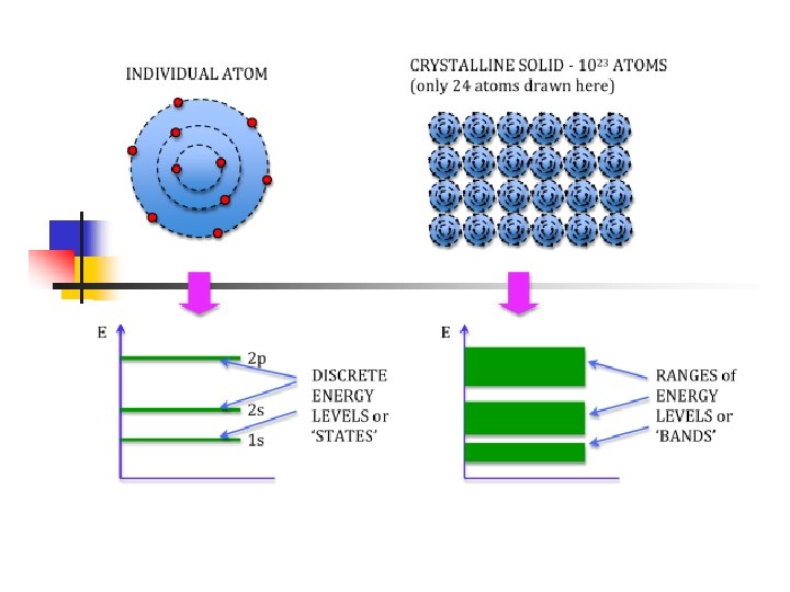
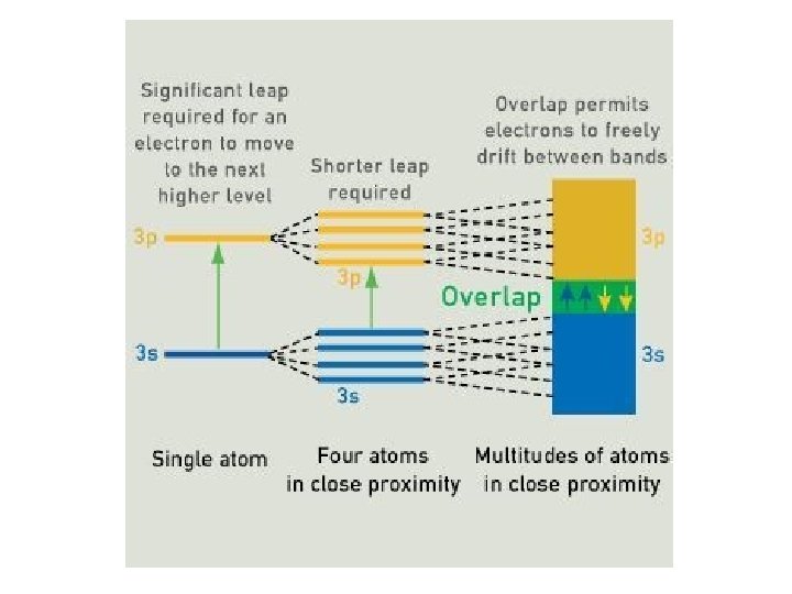

Energy bands: isolator – semiconductor - metal 1. In an isolated atom the electrons have only discrete energy levels. 2. In solid state material the atomic levels merge to energy bands. 3. In metals the conduction and the valence band overlap, whereas in isolators and semiconductors these levels are separated by an energy gap (band gap). 4. In isolators this gap is large.

Another Example https: //warwick. ac. uk/fac/sci/physics/current/postgraduate/regs/mpagswarwick/ex 5/ba ndstructure/energy_band_gaps_in_materials. jpg
")
Classification of materials based on Electrical properties (Energy band diagrams)

Semiconductors: temperature dependence

Why Silicon is more common semiconductor

Properties of intrinsic Si and Ge

Comparison of different semiconductors

Comparison of different semiconductors

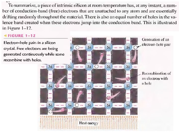
Charge carriers in semiconductors

Role of Covalent Bonds in Crystal Structure of Si Illustration of covalent bonds in Si
 Si crystal A Si atom with its four")
Example: Covalent bonds in intrinsic (undoped/pure) Si crystal A Si atom with its four valence electrons shares an electron with each of its four neighbors. This effectively creates eight shared valence electrons for each atom and produces a state of chemical stability. Also, this sharing of valence electrons produces the covalent bonds that hold the atoms together; each valence electron is attracted equally by the two adjacent atoms which share it

Bond model of semiconductors

Conduction in Semiconductors Figure: • Energy band diagram for an unexcited atom in a pure (intrinsic) silicon crystal. • There are no electrons in the conduction band. • This condition occurs only at a temperature of absolute 0 Kelvin.

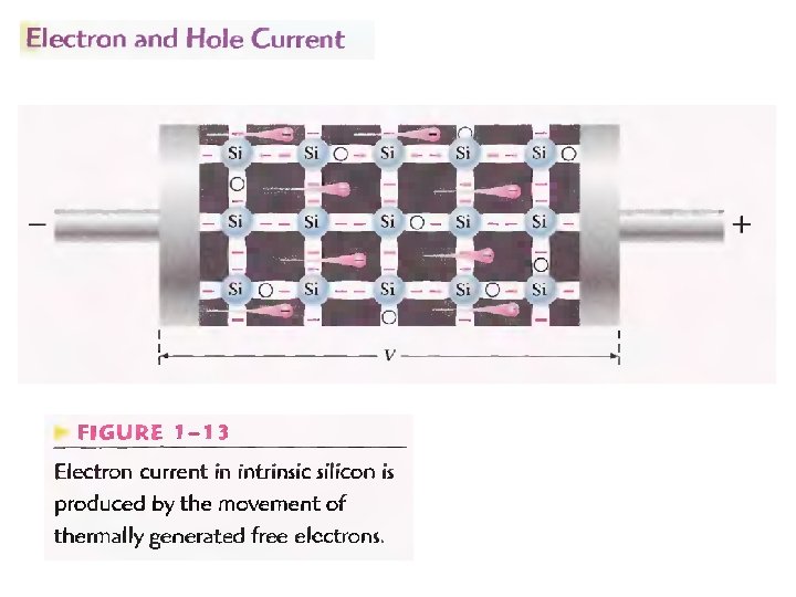
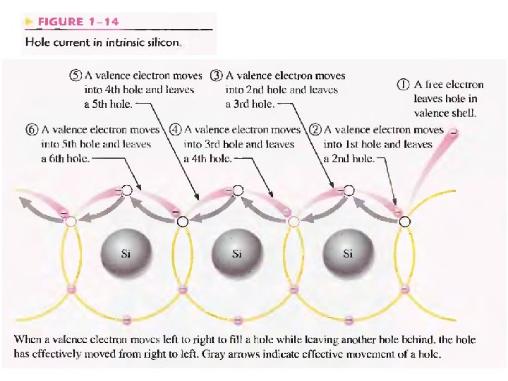
Conduction of electrons and holes in Si crystal

N-type And P-type Semiconductors

Elemental Doping of semiconductors

Example: n-type doped semiconductors

Bond model: n-doping in silicon

Band model: n-doping in silicon

p-type doped semiconductors

Band model: p-doping in silicon

Band model: p-doping in silicon

Example of N-type And P-type Semiconductors is Diode
")
The Diode (pn Junction)

Depletion Region and Barrier potential

Energy Diagrams of the PN Junction and Depletion Region
 The resistor “ R” limits the current to a")
Biasing of PN junction (diode) The resistor “ R” limits the current to a value that will not damage the diode
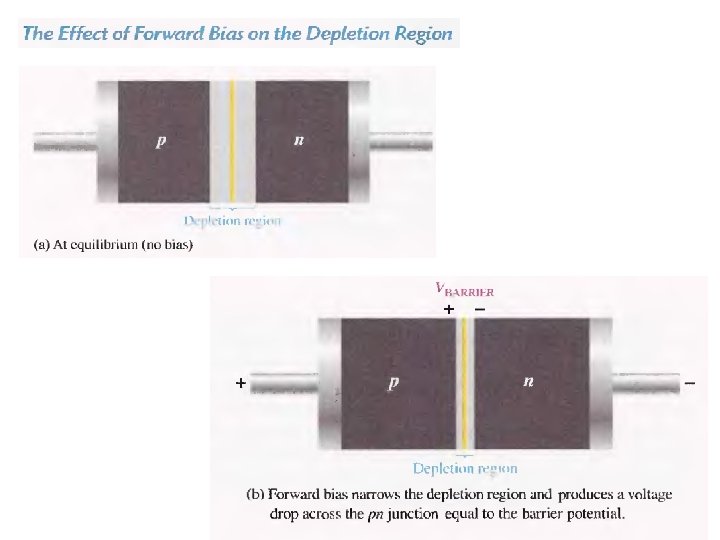
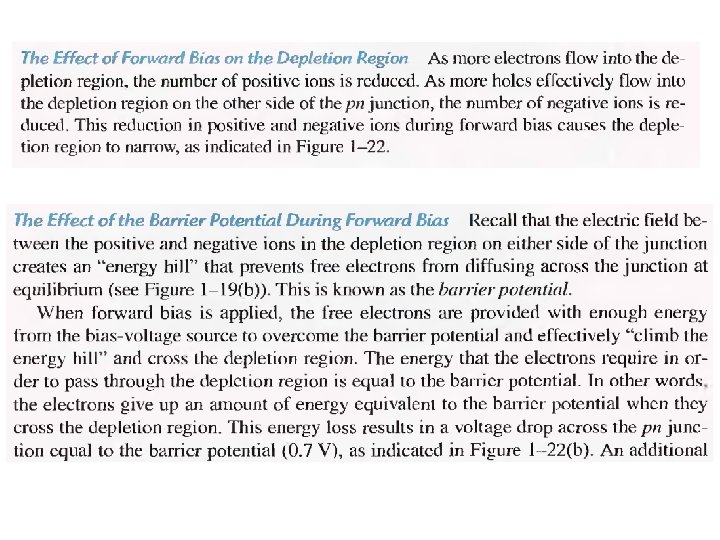

p-n junction: forward bias Applying an external voltage V with the anode to p and the cathode to n e- and holes are refilled to the depletion zone. The depletion zone becomes narrower. The potential barrier becomes smaller by e. V and diffusion across the junction becomes easier. The current across the junction increases significantly.
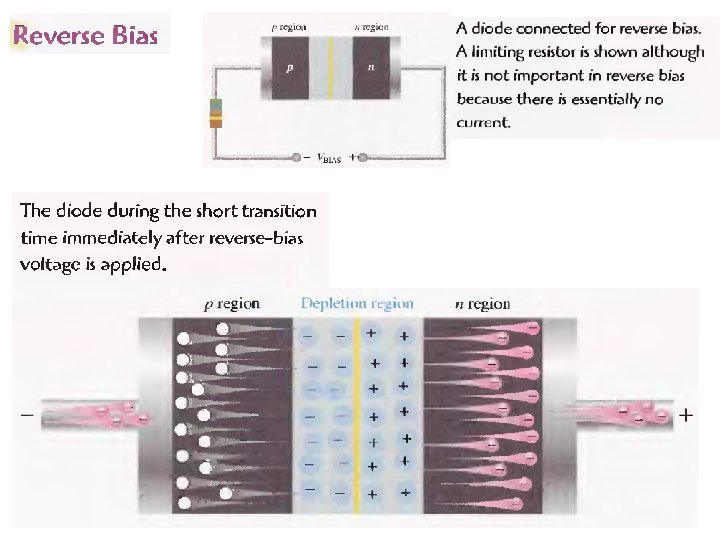

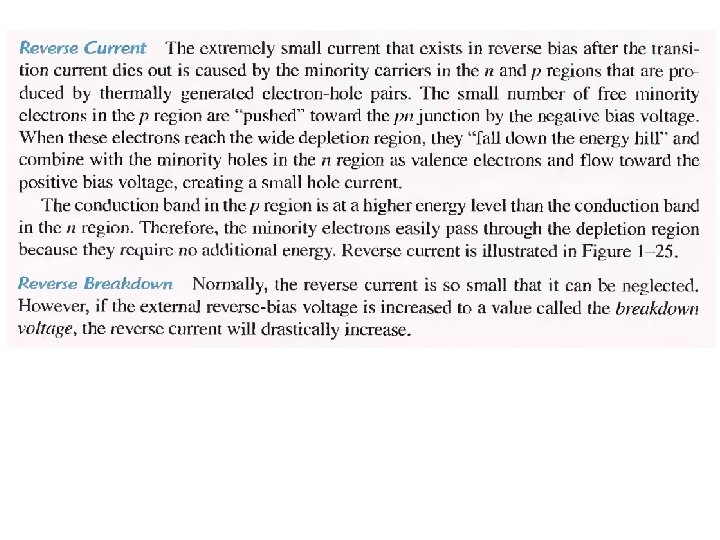

p-n junction: reverse bias Applying an external voltage V with the cathode to p and the anode to n e- and holes are pulled out of the Depletion zone. The depletion zone becomes larger. The potential barrier becomes higher by e. V and diffusion across the junction is suppressed. The current across the junction is very small “leakage current”.

60

Basic Transistor Operation
- Slides: 61