Lecture No 7 Logic Gates Recap n n
- Slides: 27

Lecture No. 7 Logic Gates

Recap n n n Integrated Circuits ICs Transistors Implementation technologies Switching speed Power dissipation Circuit density

Recap n Implementation Technologies CMOS TTL ECL PMOS & NMOS n E 2 CMOS n n

Operational Characteristics n n n DC Supply Voltage Noise Margin Power Dissipation Frequency Response Fan Out

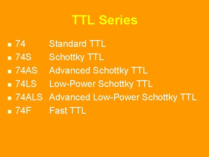
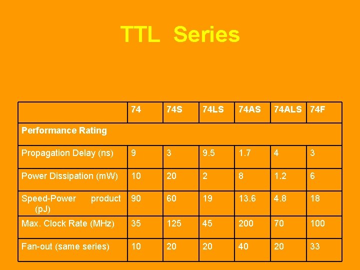
TTL Series n n n 74 74 S 74 AS 74 LS 74 ALS 74 F Standard TTL Schottky TTL Advanced Schottky TTL Low-Power Schottky TTL Advanced Low-Power Schottky TTL Fast TTL

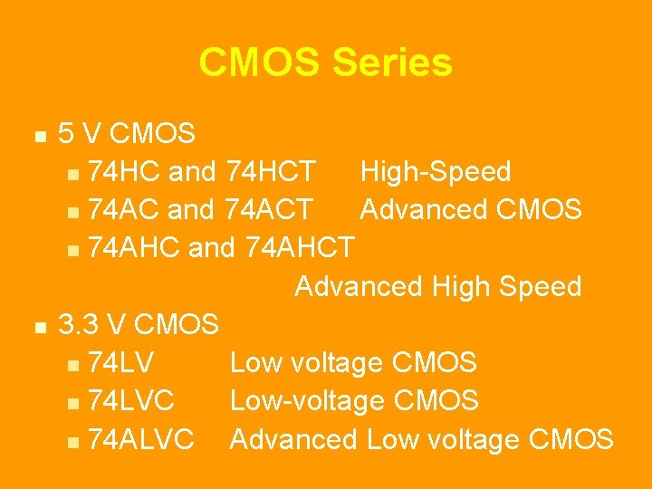
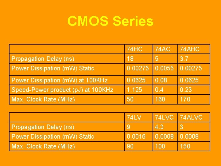
CMOS Series n n 5 V CMOS n 74 HC and 74 HCT High-Speed n 74 AC and 74 ACT Advanced CMOS n 74 AHC and 74 AHCT Advanced High Speed 3. 3 V CMOS n 74 LV Low voltage CMOS n 74 LVC Low-voltage CMOS n 74 ALVC Advanced Low voltage CMOS

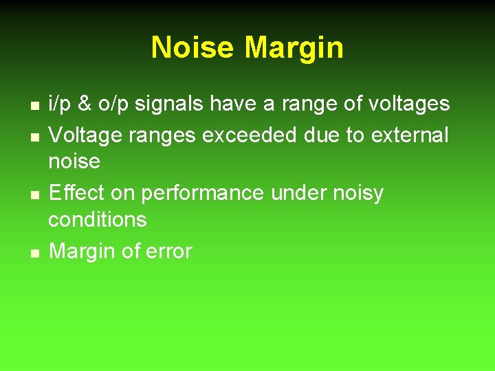
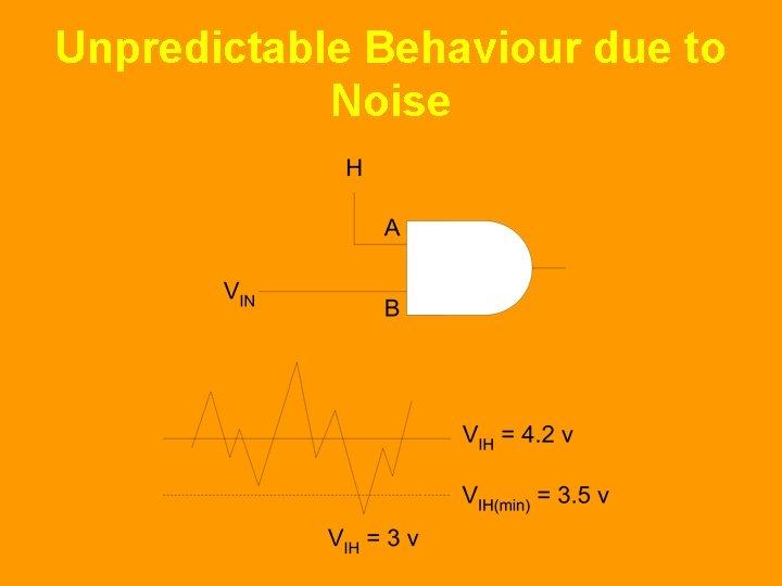
Noise Margin n n i/p & o/p signals have a range of voltages Voltage ranges exceeded due to external noise Effect on performance under noisy conditions Margin of error

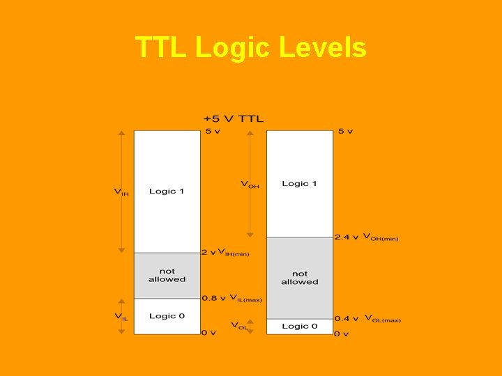
TTL Logic Levels

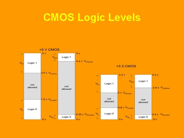
CMOS Logic Levels

Unpredictable Behaviour due to Noise

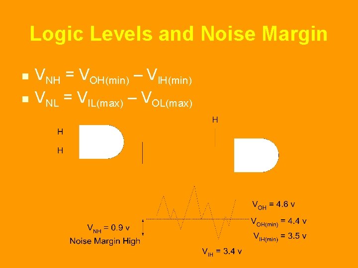
Logic Levels and Noise Margin n n VNH = VOH(min) – VIH(min) VNL = VIL(max) – VOL(max)

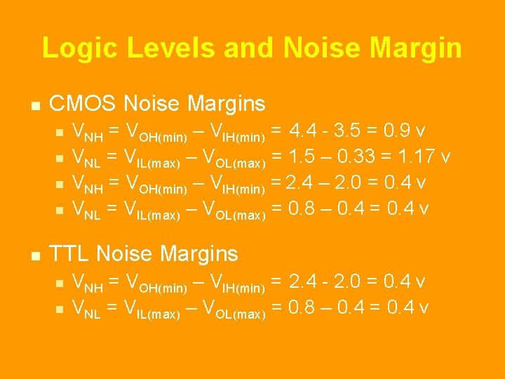
Logic Levels and Noise Margin n CMOS Noise Margins n n n VNH = VOH(min) – VIH(min) = 4. 4 - 3. 5 = 0. 9 v VNL = VIL(max) – VOL(max) = 1. 5 – 0. 33 = 1. 17 v VNH = VOH(min) – VIH(min) = 2. 4 – 2. 0 = 0. 4 v VNL = VIL(max) – VOL(max) = 0. 8 – 0. 4 = 0. 4 v TTL Noise Margins n n VNH = VOH(min) – VIH(min) = 2. 4 - 2. 0 = 0. 4 v VNL = VIL(max) – VOL(max) = 0. 8 – 0. 4 = 0. 4 v

Power Dissipation n n Power Dissipation constant for TTL Power Dissipation varies with frequency for CMOS

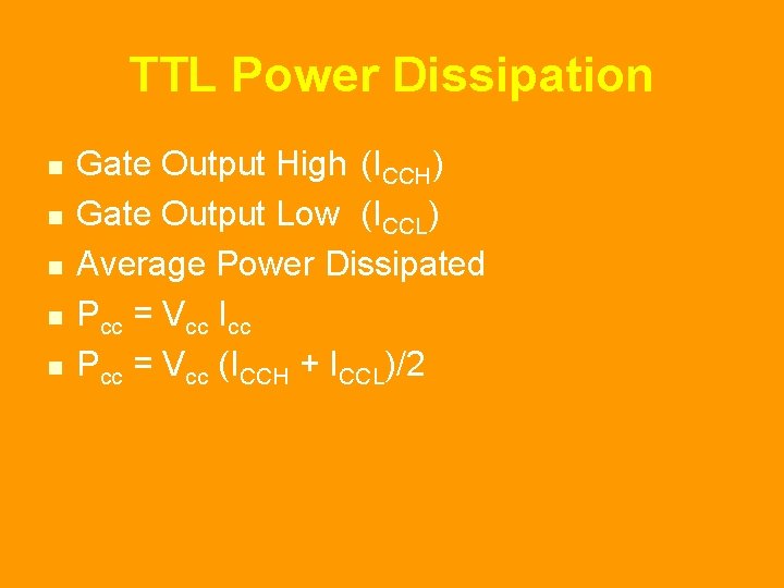
TTL Power Dissipation n n Gate Output High (ICCH) Gate Output Low (ICCL) Average Power Dissipated Pcc = Vcc Icc Pcc = Vcc (ICCH + ICCL)/2

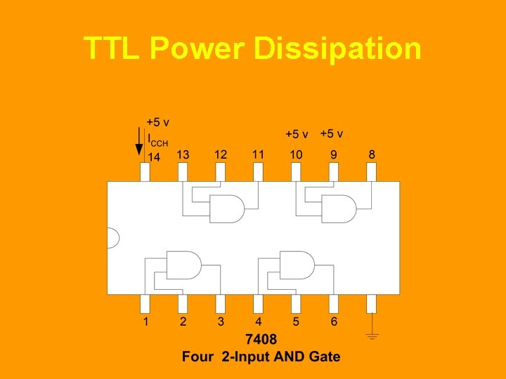
TTL Power Dissipation

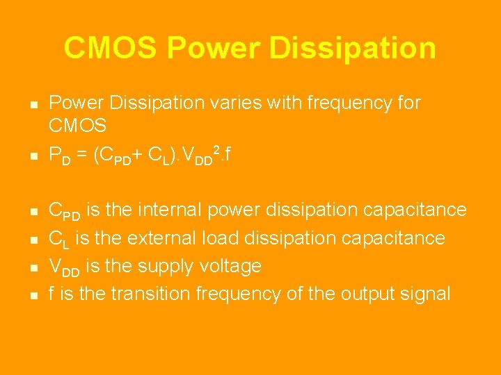
CMOS Power Dissipation n n n Power Dissipation varies with frequency for CMOS PD = (CPD+ CL). VDD 2. f CPD is the internal power dissipation capacitance CL is the external load dissipation capacitance VDD is the supply voltage f is the transition frequency of the output signal

Propagation Delay and Frequency Response n n Propagation Delay Limits frequencies at which gate can operate

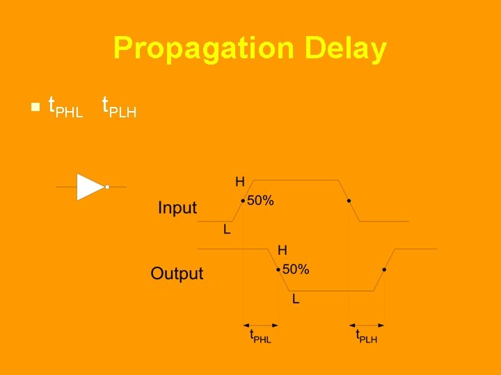
Propagation Delay n t. PHL t. PLH

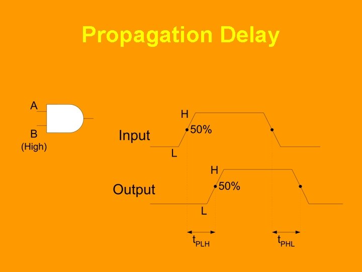
Propagation Delay

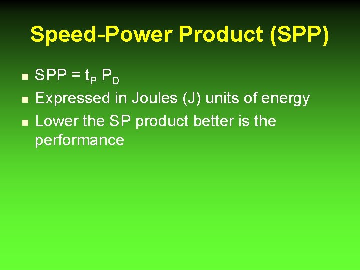
Speed-Power Product (SPP) n n n SPP = t. P PD Expressed in Joules (J) units of energy Lower the SP product better is the performance

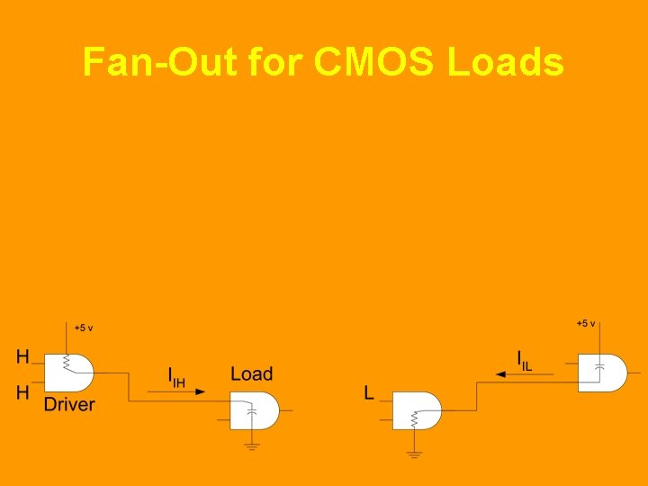
Fan-Out n n Number of same series gates that a gate can drive. Fan-Out for TTL circuits is fixed Fan-Out for CMOS circuits is related to operational frequency. Fan-Out decreases with increased frequency

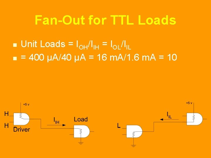
Fan-Out for TTL Loads n n Unit Loads = IOH/IIH = IOL/IIL = 400 μA/40 μA = 16 m. A/1. 6 m. A = 10

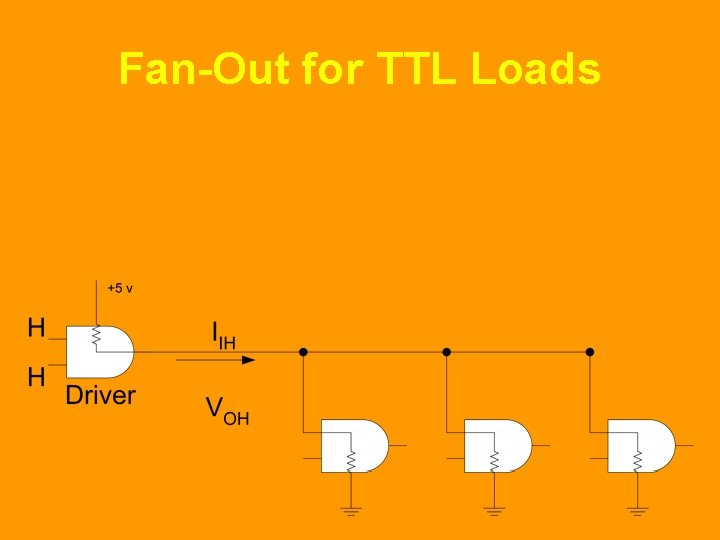
Fan-Out for TTL Loads

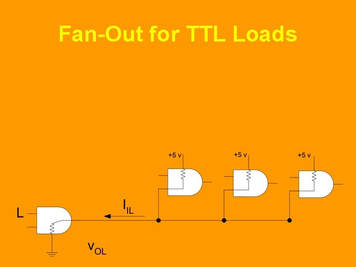
Fan-Out for TTL Loads

Fan-Out for CMOS Loads

TTL Series 74 74 S 74 LS 74 ALS 74 F Propagation Delay (ns) 9 3 9. 5 1. 7 4 3 Power Dissipation (m. W) 10 20 2 8 1. 2 6 Speed-Power (p. J) 90 60 19 13. 6 4. 8 18 Max. Clock Rate (MHz) 35 125 45 200 70 100 Fan-out (same series) 10 20 20 40 20 33 Performance Rating product

CMOS Series 74 HC 74 AHC Propagation Delay (ns) 18 5 3. 7 Power Dissipation (m. W) Static 0. 00275 0. 0055 0. 00275 Power Dissipation (m. W) at 100 KHz 0. 0625 0. 08 0. 0625 Speed-Power product (p. J) at 100 KHz 1. 125 0. 4 0. 23 Max. Clock Rate (MHz) 50 160 170 74 LVC 74 ALVC Propagation Delay (ns) 9 4. 3 3 Power Dissipation (m. W) Static 0. 0016 0. 0008 Max. Clock Rate (MHz) 90 100 150