Lecture No 23 Sequential Logic Digital Logic Design


 Burglar Alarm (fig 1)")


 R Qt+1")


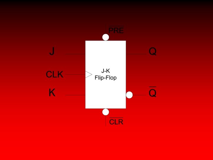
 Logic")
 Logic symbol")
 Function table (tab 5)")
 Logic symbol asynch.")
 Function table (tab 5)")
 Set-up")
- Slides: 53
Lecture No. 23 Sequential Logic
Digital Logic & Design Dr. Waseem Ikram Lecture No. 23
Recap n n n Implementation of MUX Latch NAND based latch NOR based latch Logic symbols Timing diagrams
Latch Applications n n Switch ‘bounce’ (fig 1) Burglar Alarm (fig 1)
The output of a switch connected to Logic High
Input CL K Pu lse J K O ut pu t Qt +1 0 0 Qt 0 1 0 1
Input Output Qt+1 0 0 Invalid 0 1 1 1 0 0 1 1 Clocke d operati on
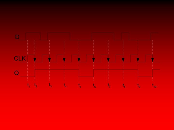
Truth-Table of Positive and Negative Edge triggered D flip-flops Input Ou t p u t CL D K Qt+ 0 X 1 t p u t CL D K Qt+ Qt 0 X Qt 1 X Qt ↑ 0 0 ↓ 0 0 ↑ 1 1 ↓ 1 1
Timing diagram of a Negative Edge triggered S-R flip-flop
Timing diagram of a Positive Edge triggered S-R flip-flop
Input CLK 0 1 ↓ ↓ Output S x x 0 0 1 1 R x x 0 1 Qt+1 Qt Qt Qt 0 1 invalid
Truth-Table of Positive and Negative Edge triggered S-R flip-flops Input CLK 0 1 ↑ ↑ S X X 0 0 1 1 R X X 0 1 Outp ut Qt+1 Qt Qt Qt 0 1 inval id Input CLK 0 1 ↓ ↓ S x x 0 0 1 1 R x x 0 1 Outp ut Qt+1 Qt Qt Qt 0 1 inval id
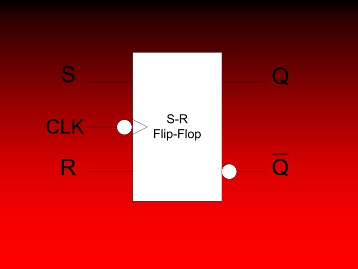
Logic Symbol of Positive and Negative edge triggered S-R flip-flops
Timing diagram of the Negative clock edge detection circuit
Negative clock edge detection circuit
Timing diagram of the Positive clock edge detection circuit
Positive clock edge detection circuit
Gated D-latch used to store parallel data
Timing diagram of a gated D latch
Logic Symbol of a Gated D Latch D Q Gated EN D Latch Q
Truth-Table of a gated D Latch Input Outp ut EN S (D) R Qt+1 0 x X Qt 1 0 0 Qt 1 0 1 1 Invali d Input EN D Ou t p u t Qt+ 1 0 x Qt 1 0 0
Gated D Latch
Timing diagram of a gated S-R latch
Truth-Table of a gated S-R Latch Input EN S R Ou t p u t Qt+ 1 0 x x Qt 1 0 0 Qt 1 0
Logic Symbol of a Gated S-R Latch
Gated S-R Latch
The switch connected through an SR latch
The switch connected through an S-R latch
The output of a switch connected to Logic High
Edge triggered flop-flop n n n n n Gated S-R latch (fig 2) Logic symbol (fig 3) Function table (tab 1) Timing diagram (fig 4) Gated D latch (fig 5) Logic symbol (fig 6) Function table (tab 2) Timing diagram (fig 7) D-latch parallel data storage (fig 8)
Edge triggered flip-flop n n n n Edge detection circuit (fig 9) Logic symbol S-R flip-flop (fig 10) Function table (tab 3) Timing diagram (fig 11) Logic symbol D flip-flop (fig 12) Function table (tab 4) Timing diagram (fig 13)
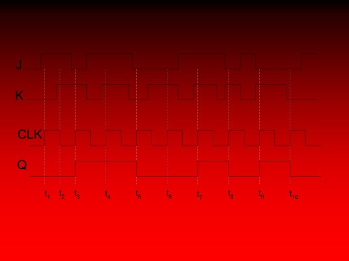
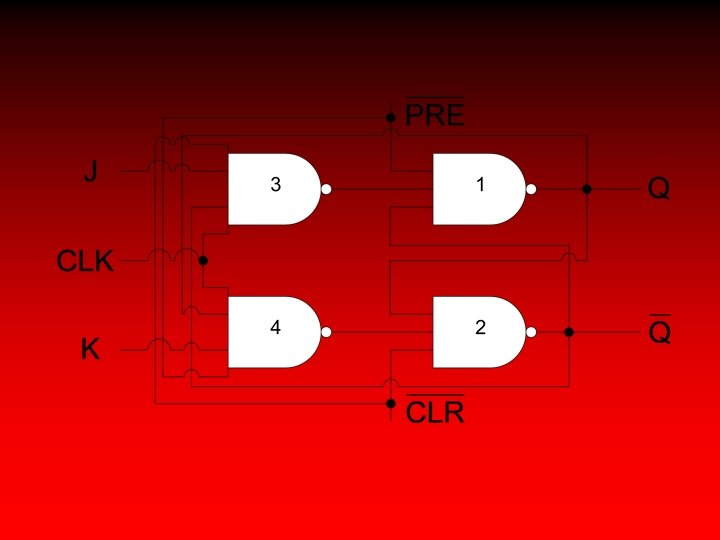
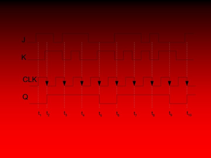
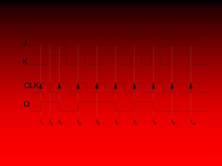
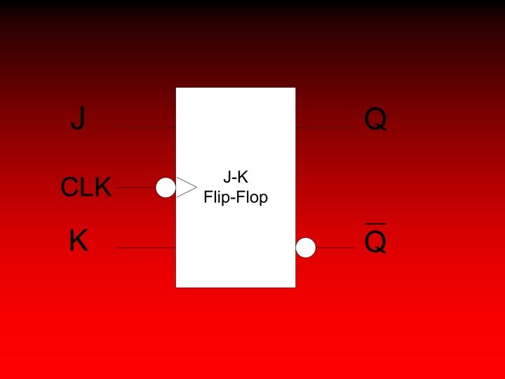
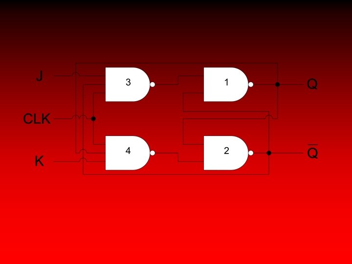
Edge triggered J-K flip-flop n n J-K flip-flop (fig 14) Function table (tab 5) Logic symbol J-K flip-flop (fig 15) Timing diagram (fig 16)
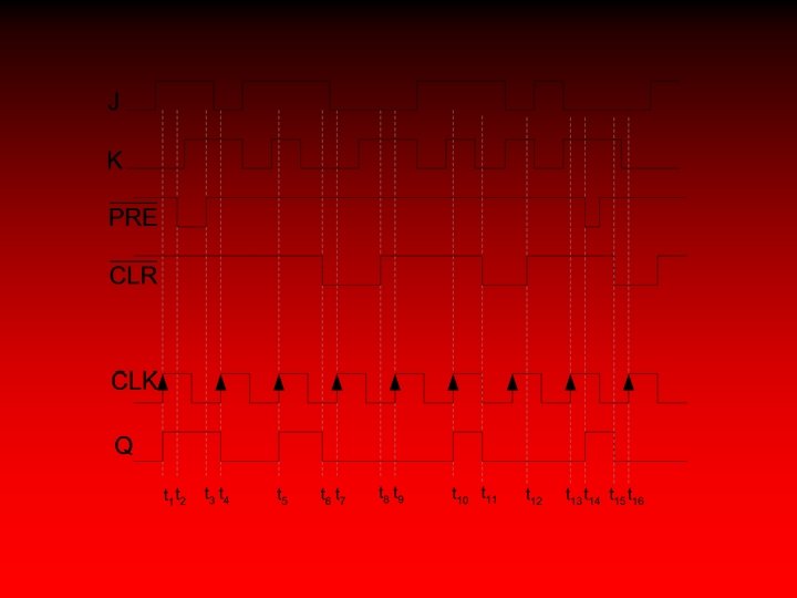
Asynchronous Inputs n n J-K flip-flop with asynch. inputs (fig 8) Logic symbol asynch. J-K flip-flop (fig 9) Function table (tab 4) Timing diagram (fig 10)
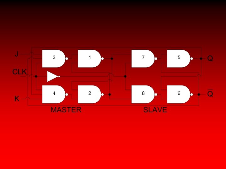
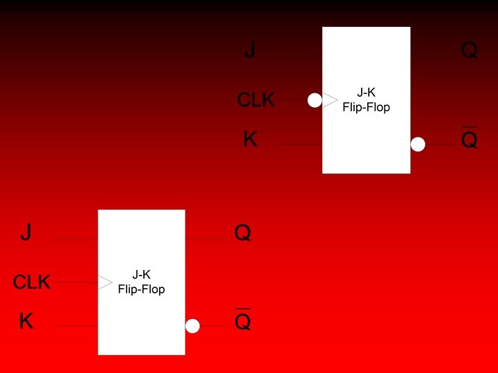
Master-Slave flip-flop n n n Master-Slave J-K flip-flop (fig 11) Function table (tab 5) Timing diagram (fig 12)
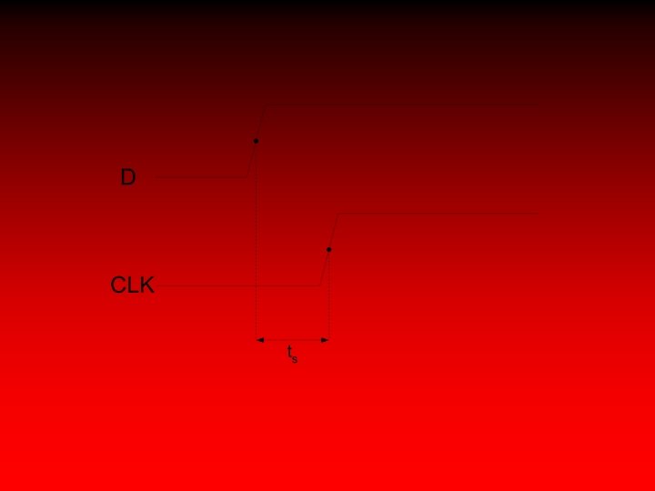
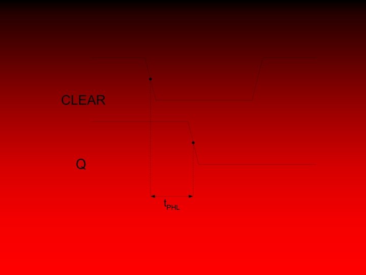
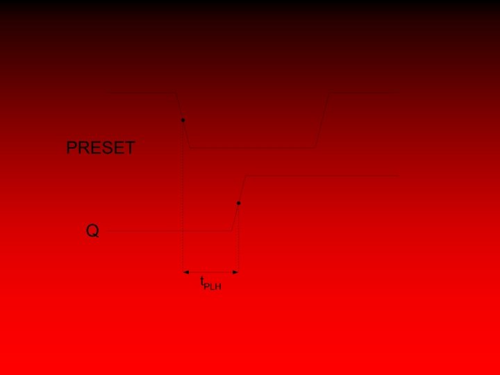
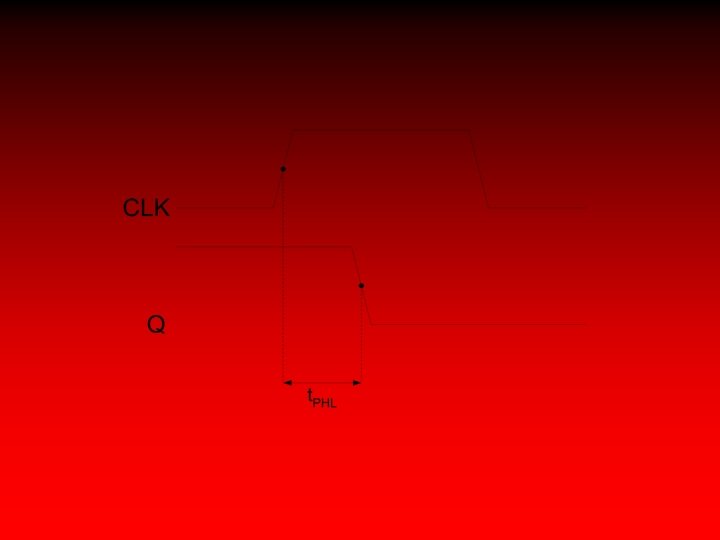
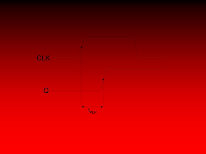
Flip-flop Operating Characteristics n n n Propagation Delay (fig 13, 14, 15, 16) Set-up Time (fig 17) Hold Time (fig 18) Maximum clock frequency Pulse width Power Dissipation