Lecture 9 Combinational Automatic TestPattern Generation ATPG Basics
Lecture 9 Combinational Automatic Test-Pattern Generation (ATPG) Basics n n n n Algorithms and representations Structural vs. functional test Definitions Search spaces Completeness Algebras Types of Algorithms Copyright 2001, Agrawal & Bushnell VLSI Test: Lecture 9 1
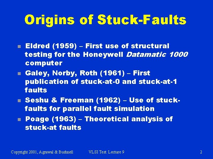
Origins of Stuck-Faults n n Eldred (1959) – First use of structural testing for the Honeywell Datamatic 1000 computer Galey, Norby, Roth (1961) – First publication of stuck-at-0 and stuck-at-1 faults Seshu & Freeman (1962) – Use of stuckfaults for parallel fault simulation Poage (1963) – Theoretical analysis of stuck-at faults Copyright 2001, Agrawal & Bushnell VLSI Test: Lecture 9 2

Functional vs. Structural ATPG Copyright 2001, Agrawal & Bushnell VLSI Test: Lecture 9 3

Carry Circuit Copyright 2001, Agrawal & Bushnell VLSI Test: Lecture 9 4

Functional vs. Structural (Continued) n n n Functional ATPG – generate complete set of tests for circuit input-output combinations § 129 inputs, 65 outputs: § 2129 = 680, 564, 733, 841, 876, 926, 749, 214, 863, 536, 422, 912 patterns § Using 1 GHz ATE, would take 2. 15 x 1022 years Structural test: § No redundant adder hardware, 64 bit slices § Each with 27 faults (using fault equivalence) § At most 64 x 27 = 1728 faults (tests) § Takes 0. 000001728 s on 1 GHz ATE Designer gives small set of functional tests – augment with structural tests to boost coverage to 98 + % Copyright 2001, Agrawal & Bushnell VLSI Test: Lecture 9 5

Definition of Automatic Test-Pattern Generator n n n Operations on digital hardware: § Inject fault into circuit modeled in computer § Use various ways to activate and propagate fault effect through hardware to circuit output § Output flips from expected to faulty signal Electron-beam (E-beam) test observes internal signals – “picture” of nodes charged to 0 and 1 in different colors § Too expensive Scan design – add test hardware to all flip-flops to make them a giant shift register in test mode § Can shift state in, scan state out § Widely used – makes sequential test combinational § Costs: 5 to 20% chip area, circuit delay, extra pin, longer test sequence Copyright 2001, Agrawal & Bushnell VLSI Test: Lecture 9 6

Circuit and Binary Decision Tree Copyright 2001, Agrawal & Bushnell VLSI Test: Lecture 9 7

Binary Decision Diagram n n n BDD – Follow path from source to sink node – product of literals along path gives Boolean value at sink Rightmost path: A B C = 1 Problem: Size varies greatly with variable order Copyright 2001, Agrawal & Bushnell VLSI Test: Lecture 9 8

Algorithm Completeness n n n Definition: Algorithm is complete if it ultimately can search entire binary decision tree, as needed, to generate a test Untestable fault – no test for it even after entire tree searched Combinational circuits only – untestable faults are redundant, showing the presence of unnecessary hardware Copyright 2001, Agrawal & Bushnell VLSI Test: Lecture 9 9
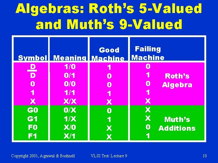
Algebras: Roth’s 5 -Valued and Muth’s 9 -Valued Failing Good Symbol Meaning Machine 0 D 1/0 1 1 D 0/1 0 Roth’s 0 0 0/0 0 Algebra 1 1 1/1 1 X X X/X X X G 0 0/X 0 X G 1 1/X 1 Muth’s 0 Additions F 0 X/0 X 1 F 1 X/1 X Copyright 2001, Agrawal & Bushnell VLSI Test: Lecture 9 10
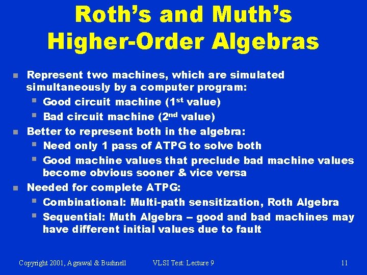
Roth’s and Muth’s Higher-Order Algebras n n n Represent two machines, which are simulated simultaneously by a computer program: § Good circuit machine (1 st value) § Bad circuit machine (2 nd value) Better to represent both in the algebra: § Need only 1 pass of ATPG to solve both § Good machine values that preclude bad machine values become obvious sooner & vice versa Needed for complete ATPG: § Combinational: Multi-path sensitization, Roth Algebra § Sequential: Muth Algebra -- good and bad machines may have different initial values due to fault Copyright 2001, Agrawal & Bushnell VLSI Test: Lecture 9 11
Exhaustive Algorithm n n For n-input circuit, generate all 2 n input patterns Infeasible, unless circuit is partitioned into cones of logic, with 15 inputs £ § Perform exhaustive ATPG for each cone § Misses faults that require specific activation patterns for multiple cones to be tested Copyright 2001, Agrawal & Bushnell VLSI Test: Lecture 9 12
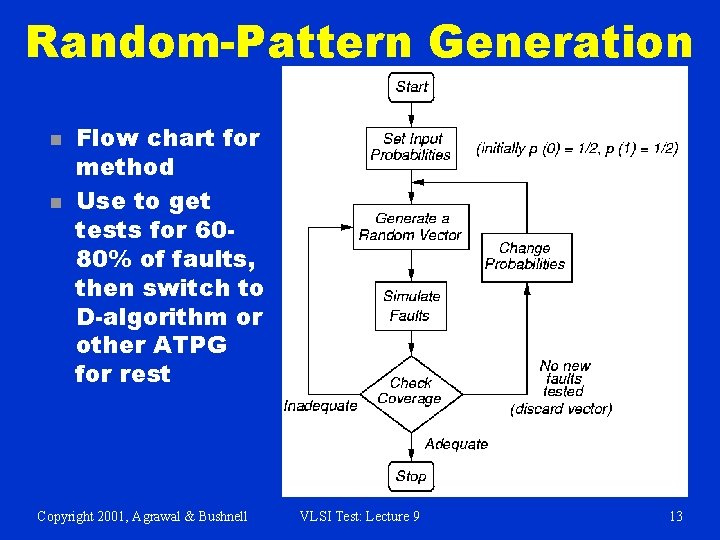
Random-Pattern Generation n n Flow chart for method Use to get tests for 6080% of faults, then switch to D-algorithm or other ATPG for rest Copyright 2001, Agrawal & Bushnell VLSI Test: Lecture 9 13
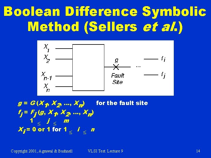
Boolean Difference Symbolic Method (Sellers et al. ) g = G (X 1, X 2, …, Xn) for the fault site fj = Fj (g, X 1, X 2, …, Xn) 1 £ j £ m Xi = 0 or 1 for 1 £ i £ n Copyright 2001, Agrawal & Bushnell VLSI Test: Lecture 9 14
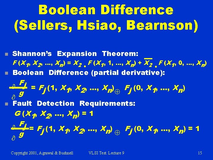
Boolean Difference (Sellers, Hsiao, Bearnson) n Shannon’s Expansion Theorem: F (X 1, X 2, …, Xn) = X 2 · F (X 1, 1, …, Xn) + X 2 F (X 1, 0, …, Xn) · n Boolean Difference (partial derivative): Fj ¶ = Fj (1, X 2, …, Xn) Fj (0, X 1, …, Xn) Å g n ¶ Fault Detection Requirements: G (X 1, X 2, …, Xn) = 1 F ¶ j = F (1, X , …, X ) Fj (0, X 1, …, Xn) = 1 j 1 2 n Å g ¶ Copyright 2001, Agrawal & Bushnell VLSI Test: Lecture 9 15
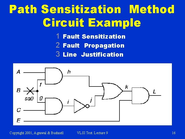
Path Sensitization Method Circuit Example 1 Fault Sensitization 2 Fault Propagation 3 Line Justification Copyright 2001, Agrawal & Bushnell VLSI Test: Lecture 9 16
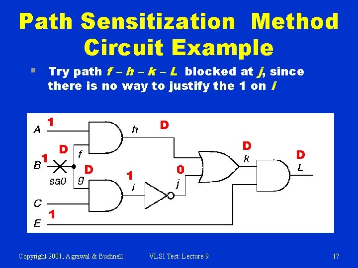
Path Sensitization Method Circuit Example § Try path f – h – k – L blocked at j, since there is no way to justify the 1 on i 1 1 D D 1 0 D 1 Copyright 2001, Agrawal & Bushnell VLSI Test: Lecture 9 17
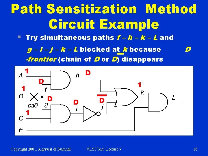
Path Sensitization Method Circuit Example § Try simultaneous paths f – h – k – L and g – i – j – k – L blocked at k because -frontier (chain of D or D) disappears 1 1 D D D 1 Copyright 2001, Agrawal & Bushnell VLSI Test: Lecture 9 18
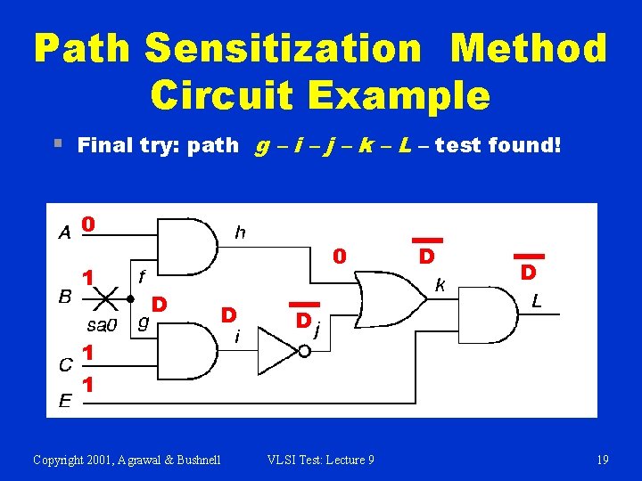
Path Sensitization Method Circuit Example § Final try: path g – i – j – k – L – test found! 0 1 0 D D D 1 1 Copyright 2001, Agrawal & Bushnell VLSI Test: Lecture 9 19
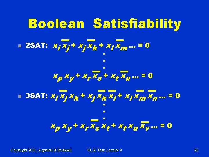
Boolean Satisfiability n n 2 SAT: xi xj + xj xk + xl xm … = 0. . . xp xy + xr xs + xt xu … = 0 3 SAT: xi xj xk + xj xk xl + xl xm xn … = 0. . . xp xy + xr xs xt + xt xu x v … = 0 Copyright 2001, Agrawal & Bushnell VLSI Test: Lecture 9 20
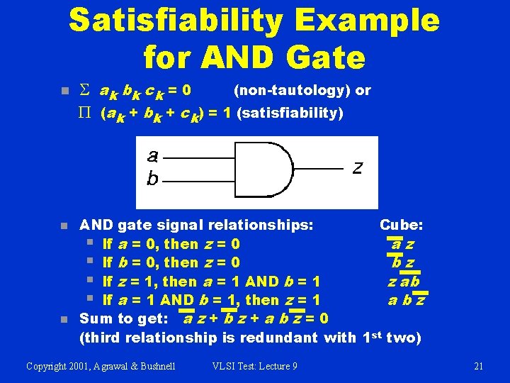
Satisfiability Example for AND Gate n n n S ak bk c k = 0 (non-tautology) or P (ak + bk + ck) = 1 (satisfiability) AND gate signal relationships: Cube: § If a = 0, then z = 0 az § If b = 0, then z = 0 bz § If z = 1, then a = 1 AND b = 1 z ab § If a = 1 AND b = 1, then z = 1 abz Sum to get: a z + b z + a b z = 0 (third relationship is redundant with 1 st two) Copyright 2001, Agrawal & Bushnell VLSI Test: Lecture 9 21
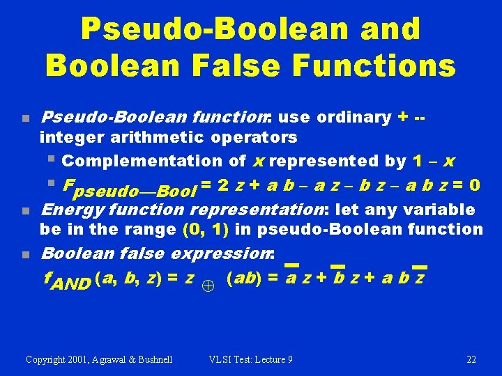
Pseudo-Boolean and Boolean False Functions n n n Pseudo-Boolean function: use ordinary + -- integer arithmetic operators § Complementation of x represented by 1 – x § Fpseudo—Bool = 2 z + a b – a z – b z – a b z = 0 Energy function representation: let any variable be in the range (0, 1) in pseudo-Boolean function Boolean false expression: f. AND (a, b, z) = z Å (ab) = a z + b z + a b z Copyright 2001, Agrawal & Bushnell VLSI Test: Lecture 9 22
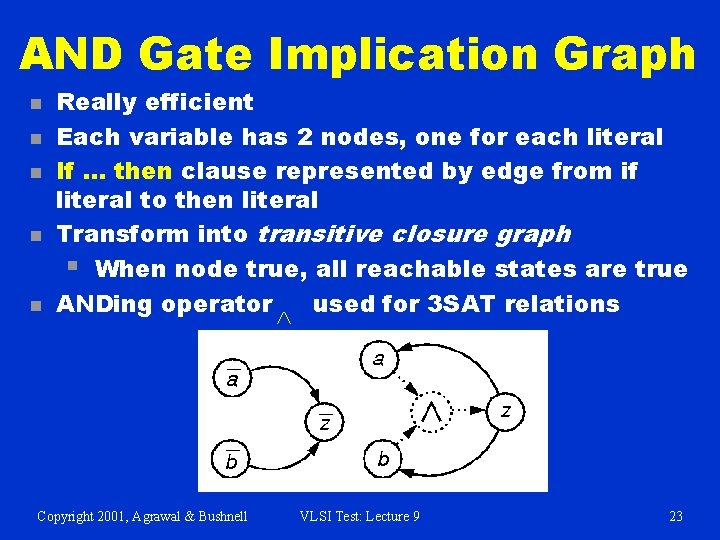
AND Gate Implication Graph n n n Really efficient Each variable has 2 nodes, one for each literal If … then clause represented by edge from if literal to then literal Transform into transitive closure graph § When node true, all reachable states are true ANDing operator used for 3 SAT relations Ù Ù Copyright 2001, Agrawal & Bushnell VLSI Test: Lecture 9 23
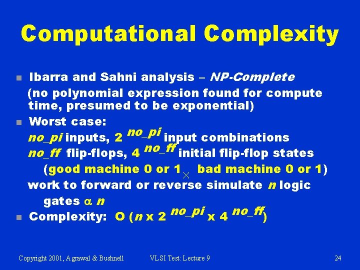
Computational Complexity n n n Ibarra and Sahni analysis – NP-Complete (no polynomial expression found for compute time, presumed to be exponential) Worst case: no_pi inputs, 2 no_pi input combinations no_ff flip-flops, 4 no_ff initial flip-flop states (good machine 0 or 1 ´ bad machine 0 or 1) work to forward or reverse simulate n logic gates a n Complexity: O (n x 2 no_pi x 4 no_ff) Copyright 2001, Agrawal & Bushnell VLSI Test: Lecture 9 24
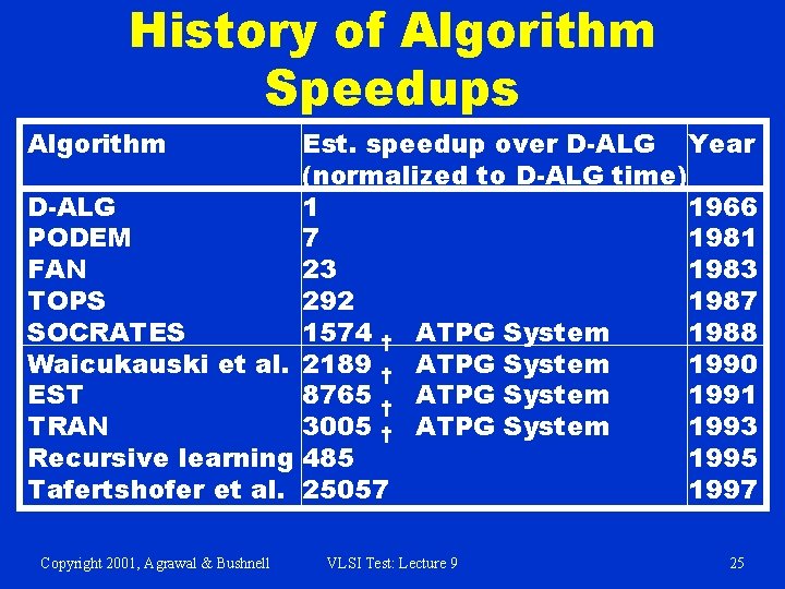
History of Algorithm Speedups Algorithm Est. speedup over D-ALG Year (normalized to D-ALG time) D-ALG 1 1966 PODEM 7 1981 FAN 23 1983 TOPS 292 1987 SOCRATES 1574 † ATPG System 1988 Waicukauski et al. 2189 † ATPG System 1990 EST 8765 † ATPG System 1991 TRAN 3005 † ATPG System 1993 Recursive learning 485 1995 Tafertshofer et al. 25057 1997 Copyright 2001, Agrawal & Bushnell VLSI Test: Lecture 9 25
Analog Fault Modeling Impractical for Logic ATPG n n n Huge # of different possible analog faults in digital circuit Exponential complexity of ATPG algorithm – a 20 flip-flop circuit can take days of computing § Cannot afford to go to a lower-level model Most test-pattern generators for digital circuits cannot even model at the transistor switch level (see textbook for 5 examples of switch-level ATPG) Copyright 2001, Agrawal & Bushnell VLSI Test: Lecture 9 26
- Slides: 26