Lecture 8 Overview Review of Combinational Logic Technologies
Lecture 8 Overview • Review of Combinational Logic Technologies • Logic Implementation • Programmable Logic Devices 1 ENGN 3213: Digital Systems and Microprocessors L#8
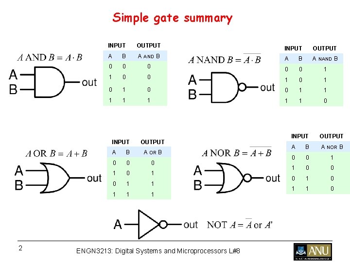
Simple gate summary INPUT OUTPUT A B A AND B A NAND B 0 0 0 1 1 0 0 1 0 1 0 0 1 1 1 1 0 INPUT 2 OUTPUT A B A OR B 0 0 0 1 0 1 1 1 ENGN 3213: Digital Systems and Microprocessors L#8 INPUT OUTPUT A B A NOR B 0 0 1 1 0
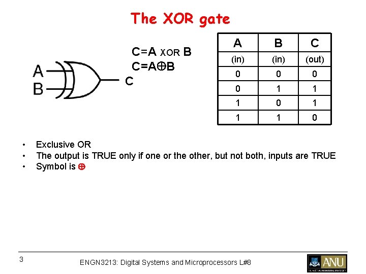
The XOR gate C=A XOR B C=A B C • • • 3 A B C (in) (out) 0 0 1 1 1 0 Exclusive OR The output is TRUE only if one or the other, but not both, inputs are TRUE Symbol is ENGN 3213: Digital Systems and Microprocessors L#8
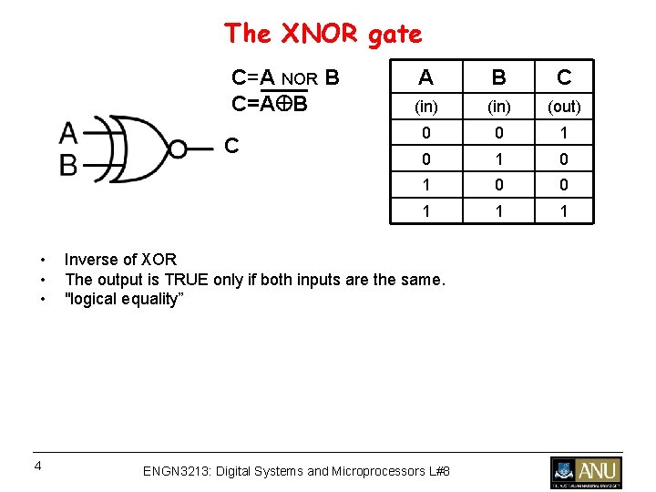
The XNOR gate C=A NOR B C=A B C • • • 4 A B C (in) (out) 0 0 1 0 1 0 0 1 1 1 Inverse of XOR The output is TRUE only if both inputs are the same. "logical equality” ENGN 3213: Digital Systems and Microprocessors L#8
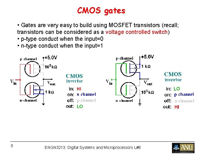
CMOS gates • Gates are very easy to build using MOSFET transistors (recall; transistors can be considered as a voltage controlled switch) • p-type conduct when the input=0 • n-type conduct when the input=1 5 ENGN 3213: Digital Systems and Microprocessors L#8
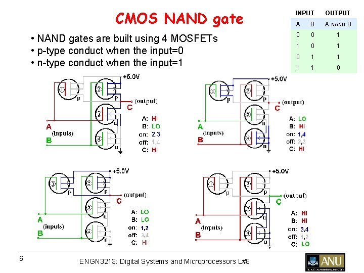
CMOS NAND gate • NAND gates are built using 4 MOSFETs • p-type conduct when the input=0 • n-type conduct when the input=1 6 ENGN 3213: Digital Systems and Microprocessors L#8 INPUT OUTPUT A B A NAND B 0 0 1 1 0
Review of Gate Processing A NOT gate inverts its single input An AND gate produces 1 if both input values are 1 An OR gate produces 0 if both input values are 0 An XOR gate produces 0 if input values are the same A NAND gate produces 0 if both inputs are 1 A NOR gate produces a 1 if both inputs are 0 7 ENGN 3213: Digital Systems and Microprocessors L#8
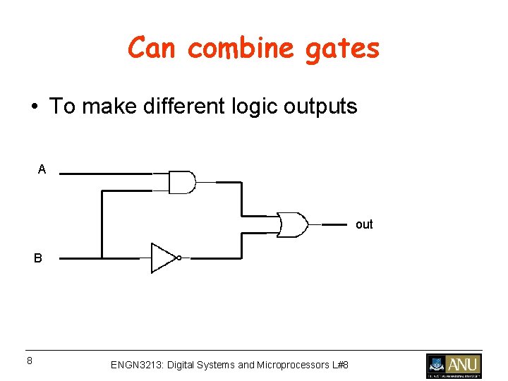
Can combine gates • To make different logic outputs A out B 8 ENGN 3213: Digital Systems and Microprocessors L#8
Logic Types • Positive Logic (active high) – 0 = 0 V. , 1 = 1. 0 V. • Negative Logic (active low) – 0 = 1. 0 V. , 1 = 0 V. • Mixed-Logic – logic with: – Negative (positive) logic inputs – Positive (negative) logic outputs – Arbitrary mixture of positive & negative logic 9 ENGN 3213: Digital Systems and Microprocessors L#8
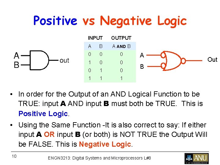
Positive vs Negative Logic INPUT OUTPUT A B A AND B 0 0 0 1 0 1 1 1 A Out B • In order for the Output of an AND Logical Function to be TRUE: input A AND input B must both be TRUE. This is Positive Logic. • Using the Same Function -It is also correct to say: If either input A OR input B (or both) is NOT TRUE the Output Will be FALSE. This is Negative Logic. 10 ENGN 3213: Digital Systems and Microprocessors L#8
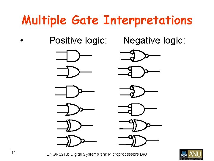
Multiple Gate Interpretations • Positive logic: Negative logic: 11 ENGN 3213: Digital Systems and Microprocessors L#8
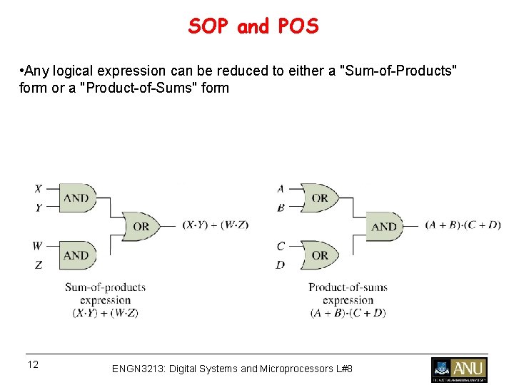
SOP and POS • Any logical expression can be reduced to either a "Sum-of-Products" form or a "Product-of-Sums" form 12 ENGN 3213: Digital Systems and Microprocessors L#8
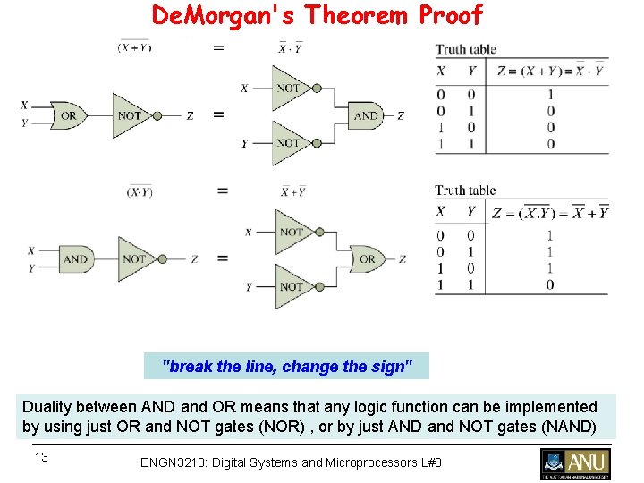
De. Morgan's Theorem Proof "break the line, change the sign" Duality between AND and OR means that any logic function can be implemented by using just OR and NOT gates (NOR) , or by just AND and NOT gates (NAND) 13 ENGN 3213: Digital Systems and Microprocessors L#8
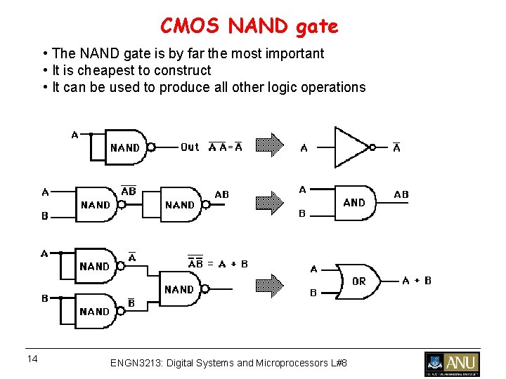
CMOS NAND gate • The NAND gate is by far the most important • It is cheapest to construct • It can be used to produce all other logic operations 14 ENGN 3213: Digital Systems and Microprocessors L#8
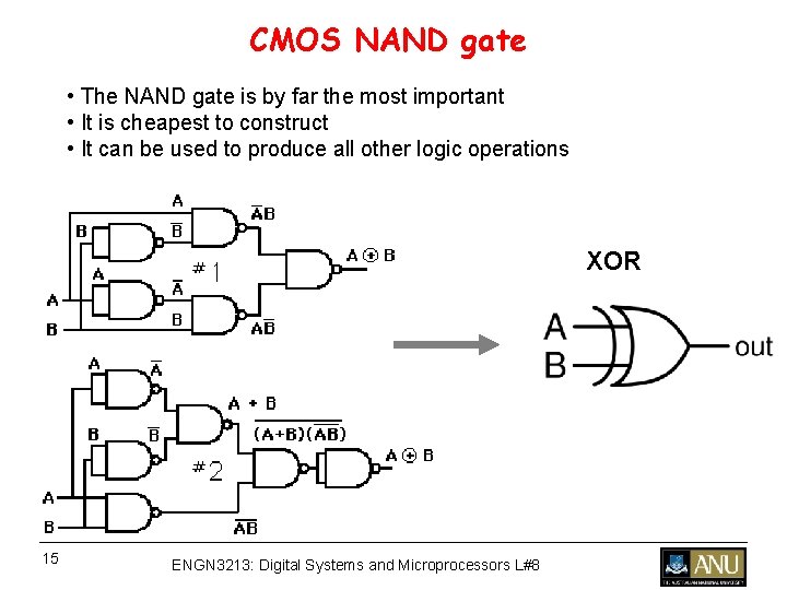
CMOS NAND gate • The NAND gate is by far the most important • It is cheapest to construct • It can be used to produce all other logic operations XOR 15 ENGN 3213: Digital Systems and Microprocessors L#8
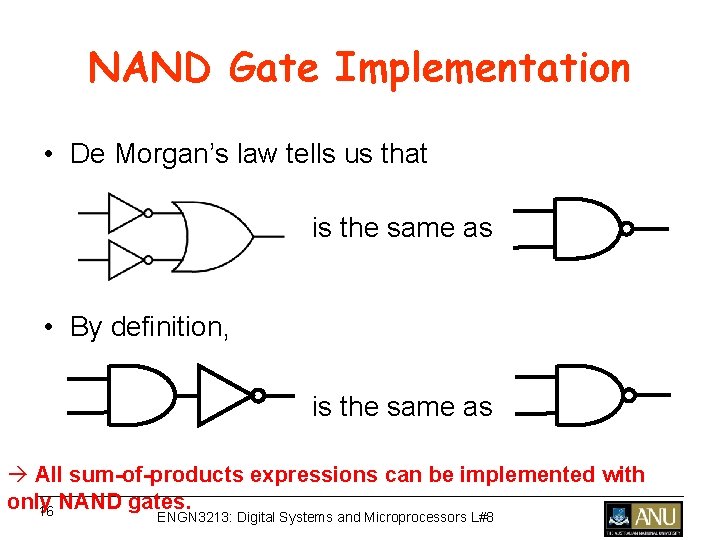
NAND Gate Implementation • De Morgan’s law tells us that is the same as • By definition, is the same as à All sum-of-products expressions can be implemented with only NAND gates. 16 ENGN 3213: Digital Systems and Microprocessors L#8
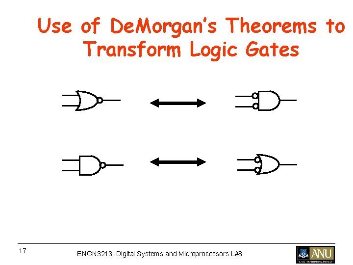
Use of De. Morgan’s Theorems to Transform Logic Gates 17 ENGN 3213: Digital Systems and Microprocessors L#8
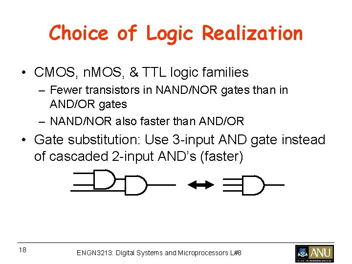
Choice of Logic Realization • CMOS, n. MOS, & TTL logic families – Fewer transistors in NAND/NOR gates than in AND/OR gates – NAND/NOR also faster than AND/OR • Gate substitution: Use 3 -input AND gate instead of cascaded 2 -input AND’s (faster) 18 ENGN 3213: Digital Systems and Microprocessors L#8
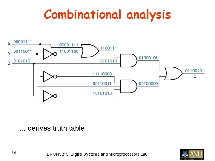
Combinational analysis . . . derives truth table 19 ENGN 3213: Digital Systems and Microprocessors L#8
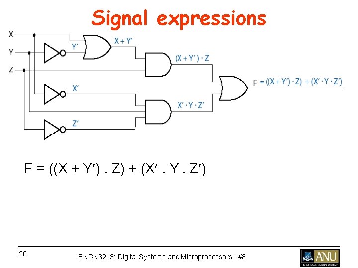
Signal expressions F = ((X + Y ). Z) + (X . Y. Z ) 20 ENGN 3213: Digital Systems and Microprocessors L#8
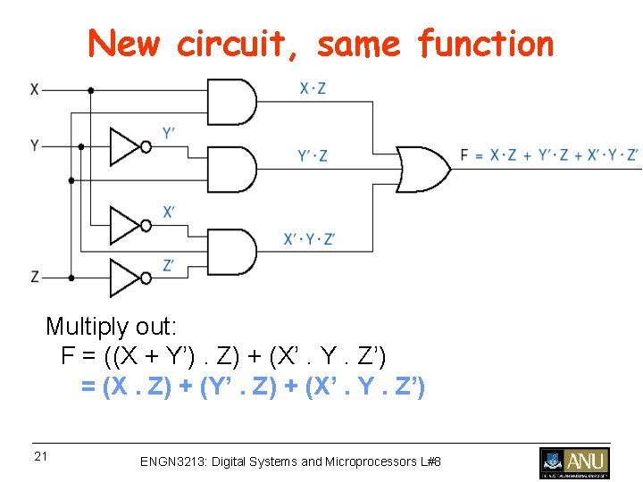
New circuit, same function Multiply out: F = ((X + Y’). Z) + (X’. Y. Z’) = (X. Z) + (Y’. Z) + (X’. Y. Z’) 21 ENGN 3213: Digital Systems and Microprocessors L#8
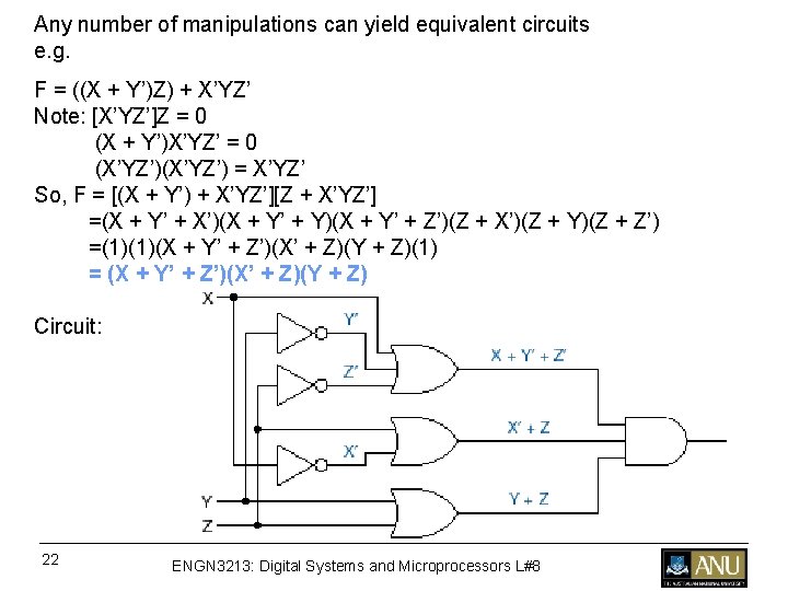
Any number of manipulations can yield equivalent circuits e. g. F = ((X + Y’)Z) + X’YZ’ Note: [X’YZ’]Z = 0 (X + Y’)X’YZ’ = 0 (X’YZ’) = X’YZ’ So, F = [(X + Y’) + X’YZ’][Z + X’YZ’] =(X + Y’ + X’)(X + Y’ + Y)(X + Y’ + Z’)(Z + X’)(Z + Y)(Z + Z’) =(1)(1)(X + Y’ + Z’)(X’ + Z)(Y + Z)(1) = (X + Y’ + Z’)(X’ + Z)(Y + Z) Circuit: 22 ENGN 3213: Digital Systems and Microprocessors L#8
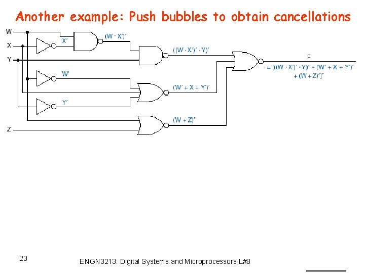
Another example: Push bubbles to obtain cancellations 23 ENGN 3213: Digital Systems and Microprocessors L#8
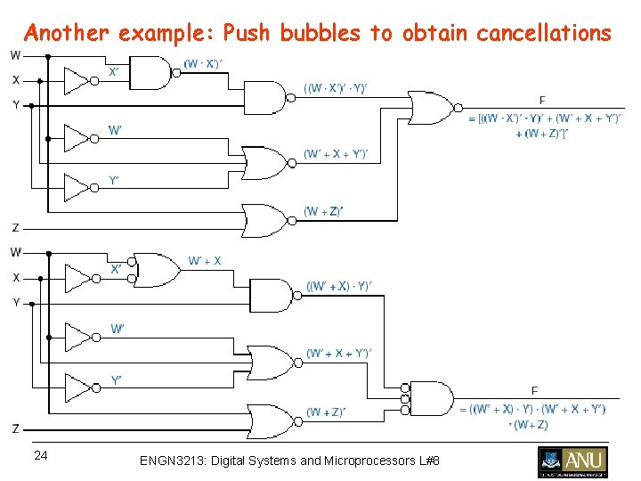
Another example: Push bubbles to obtain cancellations 24 ENGN 3213: Digital Systems and Microprocessors L#8
Conclude: given circuit ==> many equivalent equations circuit does not determine equation 25 ENGN 3213: Digital Systems and Microprocessors L#8
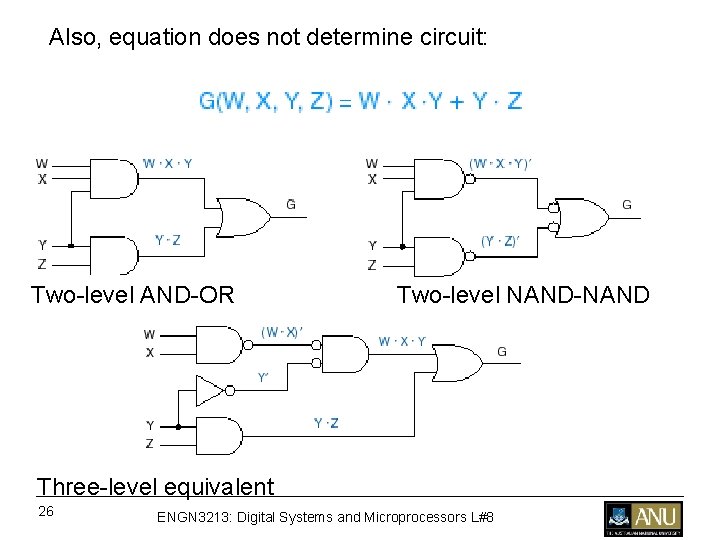
Also, equation does not determine circuit: Two-level AND-OR Two-level NAND-NAND Three-level equivalent 26 ENGN 3213: Digital Systems and Microprocessors L#8
Combinational analysis given circuit, determine function Combinational synthesis given function, determine circuit 27 ENGN 3213: Digital Systems and Microprocessors L#8
Design Considerations • In addition to logic functions, a designer must be concerned with a number of physical characteristics of digital logic circuits, including the following: – – 28 Propagation delays Gate fan-in and fan-out restrictions Power consumptions Size and weight. ENGN 3213: Digital Systems and Microprocessors L#8
Programmable Arrays of Logic Gates • Until now, we learned about designing Boolean functions using discrete logic gates • We will now describe a technique to arrange AND and OR gates (or NAND and NOR gates) into a general array structure • Specific functions can be programmed • Can use programmable logic arrays (PLA) or programmable array logic (PAL) 29 ENGN 3213: Digital Systems and Microprocessors L#8
Programmable Logic Devices • • 30 PROM (Programmable Read-only Memory) PLA (Programmable Logic Array) PAL (Programmable Array Logic) FPGA (Field-Programmable Gate Array) ENGN 3213: Digital Systems and Microprocessors L#8
Programmable Logic Device • What is a Programmable Logic Device (PLD)? – an IC that contains large numbers of gates, flip-flops and registers that are interconnected on the chip – can be configured by the user to perform a logic function – – less board space smaller enclosures faster and less costly assembly processes higher reliability (fewer ICs and circuit connections => easier troubleshooting) 31 ENGN 3213: Digital Systems and Microprocessors L#8
Programmable Logic Device • 32 Basic Ideas of PLD – A PLD consists of an array of AND gates and an array of OR gates – Each input feeds both a non-inverting buffer and an inverting buffer to produce the true and inverted forms of each variable. (i. e. the input lines to the AND-gate array) – – The AND outputs are called the product lines – Three fundamental types of standard PLDs: PROM, PAL, and PLA Each product line is connected to one of the inputs of each OR gate ENGN 3213: Digital Systems and Microprocessors L#8
PALs and PLAs Pre-fabricated building block of many AND/OR gates (or NOR, NAND) "Personalized" by making or breaking connections among the gates Programmable Array Block Diagram for Sum of Products Form 33 ENGN 3213: Digital Systems and Microprocessors L#8
Internal Structures of PLD 34 ENGN 3213: Digital Systems and Microprocessors L#8
Programmable Read-Only Memory (PROM) • Each possible minterm AND gate is present (fixed AND) plane and configurable OR plane • Can use it to do address decoding • Can also be use to implement logic functions 35 ENGN 3213: Digital Systems and Microprocessors L#8
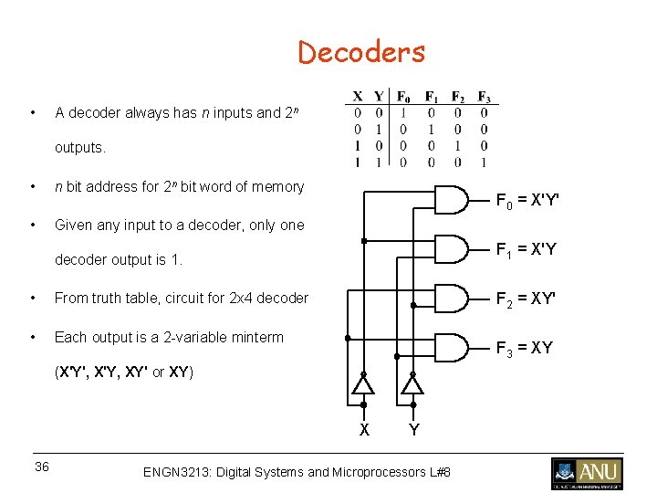
Decoders • A decoder always has n inputs and 2 n outputs. • n bit address for 2 n bit word of memory • Given any input to a decoder, only one F 0 = X'Y' decoder output is 1. F 1 = X'Y • From truth table, circuit for 2 x 4 decoder F 2 = XY' • Each output is a 2 -variable minterm F 3 = XY (X'Y', X'Y, XY' or XY) X 36 Y ENGN 3213: Digital Systems and Microprocessors L#8
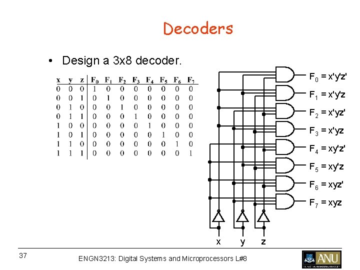
Decoders • Design a 3 x 8 decoder. F 0 = x'y'z' F 1 = x'y'z F 2 = x'yz' F 3 = x'yz F 4 = xy'z' F 5 = xy'z F 6 = xyz' F 7 = xyz x 37 y ENGN 3213: Digital Systems and Microprocessors L#8 z
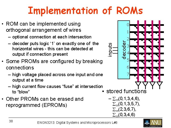
Implementation of ROMs • ROM can be implemented using orthogonal arrangement of wires • Some PROMs are configured by breaking connections – high voltage placed across one input and one output at a time – high current flow causes “fuse” at intersection • to “blow” • Other PROMs can be erased and reprogrammed (EPROMs) 38 decoder 1 inputs – optional connection at each intersection – decoder puts logic ‘ 1’ on exactly one of the horizontal wires - this can be detected at output if connection present 0 2 3 4 5 6 7 stored functions – m(0, 1, 3, 4, 6), m(0, 1, 3, 5, 7), m(2, 3, 6, 7), m(0, 3, 4, 6) ENGN 3213: Digital Systems and Microprocessors L#8
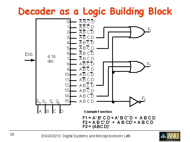
Decoder as a Logic Building Block Enb 4: 16 dec S 3 S 2 S 1 S 0 0 1 2 3 4 5 6 7 8 9 10 1 1 12 13 14 15 A B C D A B C D A B C D A B C D A B C D F 1 F 2 F 3 Example Function: F 1 = A' B' C D + A' B C' D + A B C D F 2 = A B C' D' + A B C D F 3 = (ABC D)' 39 ENGN 3213: Digital Systems and Microprocessors L#8
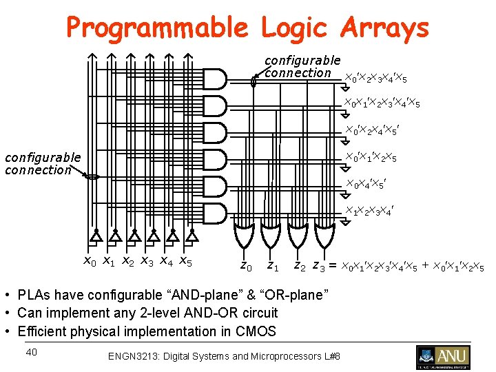
Programmable Logic Arrays configurable connection x 0 x 2 x 3 x 4 x 5 x 0 x 1 x 2 x 3 x 4 x 5 x 0 x 2 x 4 x 5 x 0 x 1 x 2 x 5 configurable connection x 0 x 4 x 5 x 1 x 2 x 3 x 4 x 0 x 1 x 2 x 3 x 4 x 5 z 0 z 1 z 2 z 3 = x 0 x 1 x 2 x 3 x 4 x 5 + x 0 x 1 x 2 x 5 • PLAs have configurable “AND-plane” & “OR-plane” • Can implement any 2 -level AND-OR circuit • Efficient physical implementation in CMOS 40 ENGN 3213: Digital Systems and Microprocessors L#8
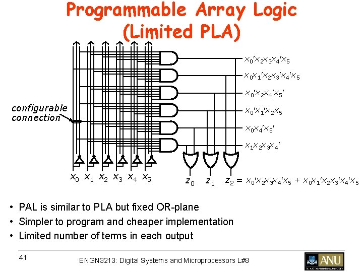
Programmable Array Logic (Limited PLA) x 0 x 2 x 3 x 4 x 5 x 0 x 1 x 2 x 3 x 4 x 5 x 0 x 2 x 4 x 5 configurable connection x 0 x 1 x 2 x 5 x 0 x 4 x 5 x 1 x 2 x 3 x 4 x 0 x 1 x 2 x 3 x 4 x 5 z 0 z 1 z 2 = x 0 x 2 x 3 x 4 x 5 + x 0 x 1 x 2 x 3 x 4 x 5 • PAL is similar to PLA but fixed OR-plane • Simpler to program and cheaper implementation • Limited number of terms in each output 41 ENGN 3213: Digital Systems and Microprocessors L#8
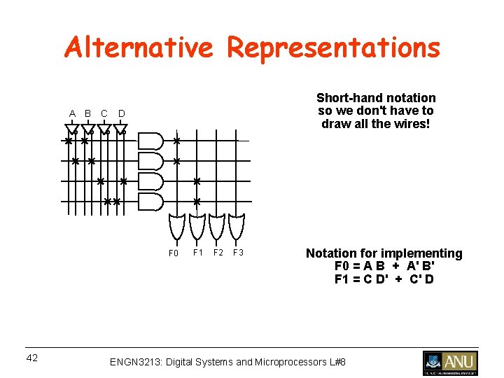
Alternative Representations A B C Short-hand notation so we don't have to draw all the wires! D F 0 42 F 1 F 2 F 3 Notation for implementing F 0 = A B + A' B' F 1 = C D' + C' D ENGN 3213: Digital Systems and Microprocessors L#8
Field Programmable Gate Arrays • FPGA roots are in the CPLDs of the 1980's • Invented by Ross Freeman (co-founder of Xilinx) in 1984. • FPGAs can be used to construct more complex circuits • Applications of FPGAs include DSP, aerospace, defense systems, computer vision, speech recognition, cryptography etc. • FPGAs especially find applications in any area or algorithm that can make use of the massive parallelism offered by their architecture. • Chip contains a large number (1, 000 s to 100, 000 s) of configurable building blocks • CAD tools map high level circuit to basic blocks, configuring function generators & other configurable elements as needed 43 ENGN 3213: Digital Systems and Microprocessors L#8
FPGA • An FPGA contains both logic blocks and programmable routing (interconnects) • A logic block is a circuit block that is replicated in an array in an FPD • A logic block consists of clusters of logic cells • Each logic cell contains a Look up table (LUT). – They are called Configurable Logic Blocks (CLB) by Xilinx. – based on Look-Up Tables. Most commercial FPGAs have 4 -input LUTs – The logic blocks of most SRAM-based FPGAs consist of logic cells – A logic cell consists of a LUT, a flip flop, and connection to adjacent cells. – A logic slice consists of 2 logic cells. – Xilinx counts closer to 2. 25 logic cells per slice because they can do more per configurable logic block (CLB) than other architectures 44 ENGN 3213: Digital Systems and Microprocessors L#8
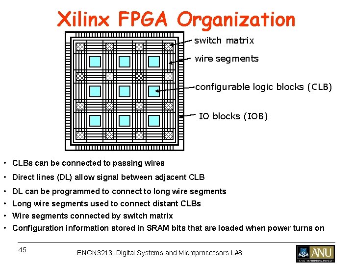
Xilinx FPGA Organization switch matrix wire segments configurable logic blocks (CLB) IO blocks (IOB) • CLBs can be connected to passing wires • Direct lines (DL) allow signal between adjacent CLB • DL can be programmed to connect to long wire segments • Long wire segments used to connect distant CLBs • Wire segments connected by switch matrix • Configuration information stored in SRAM bits that are loaded when power turns on 45 ENGN 3213: Digital Systems and Microprocessors L#8
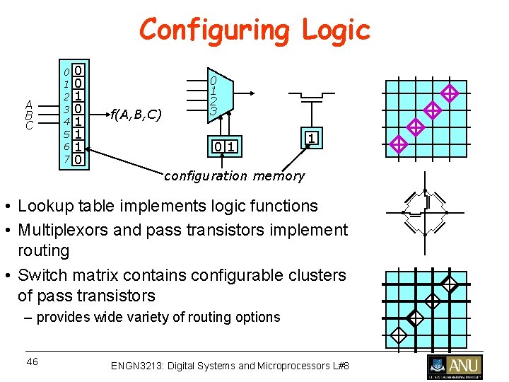
Configuring Logic A B C 0 1 2 3 4 5 6 7 0 0 1 1 1 0 f(A, B, C) 0 1 2 3 01 1 configuration memory • Lookup table implements logic functions • Multiplexors and pass transistors implement routing • Switch matrix contains configurable clusters of pass transistors – provides wide variety of routing options 46 ENGN 3213: Digital Systems and Microprocessors L#8
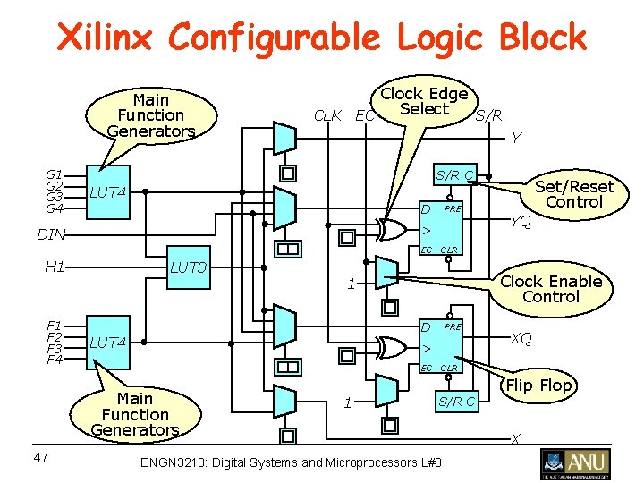
Xilinx Configurable Logic Block Main Function Generators G 1 G 2 G 3 G 4 Clock Edge Select CLK EC S/R Y S/R C Set/Reset Control LUT 4 D PRE > DIN YQ EC CLR H 1 F 2 F 3 F 4 LUT 3 D LUT 4 PRE > XQ EC CLR Main Function Generators 47 Clock Enable Control 1 1 S/R C ENGN 3213: Digital Systems and Microprocessors L#8 Flip Flop X
Things You Should Know • ROMS – Each possible minterm AND gate is present (fixed AND) plane and configurable OR plane – how large a ROM is needed for given set of logic equations? • PLAs – Limited number of AND gates – Programmable AND and OR gates. • PALs – Programmable AND plane – how are logic functions represented? • FPGAs – components of FPGA and how they relate to each other – components of typical logic cell (Configurable Logic Block) – how circuits can be mapped onto CLBs 48 ENGN 3213: Digital Systems and Microprocessors L#8
- Slides: 48