Lecture 8 OUTLINE OpAmp ckts continued examples Inverting
- Slides: 12

Lecture #8 • • • OUTLINE Op-Amp ckts continued: examples Inverting amplifier circuit Summing amplifier circuit Noninverting amplifier circuit Differential amplifier circuit Reading Chapter 14, also refer to Ch. 11 EECS 40, Spring 2004 Lecture 8, Slide 1 Prof. Sanders

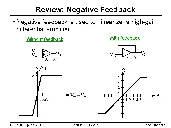
Review: Negative Feedback • Negative feedback is used to “linearize” a high-gain differential amplifier. With feedback + V V+ V 0 + Without feedback VIN V 0(V) V 0 5 5 4 3 2 1 1 2345 VIN 5 EECS 40, Spring 2004 Lecture 8, Slide 2 Prof. Sanders

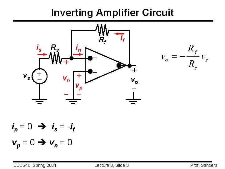
Inverting Amplifier Circuit in + – + vs vn + vp – – + Rs if – is Rf + vo – in = 0 is = -if vp = 0 vn = 0 EECS 40, Spring 2004 Lecture 8, Slide 3 Prof. Sanders

Analysis using Realistic Op Amp Model • In the analysis on the previous slide, the op amp was assumed to be ideal, i. e. Ri = ; A = ; Ro = 0 • In reality, an op amp has finite Ri, finite A, nonzero Ro, and usually is loaded at its output terminals with a load resistance RL. EECS 40, Spring 2004 Lecture 8, Slide 4 Prof. Sanders

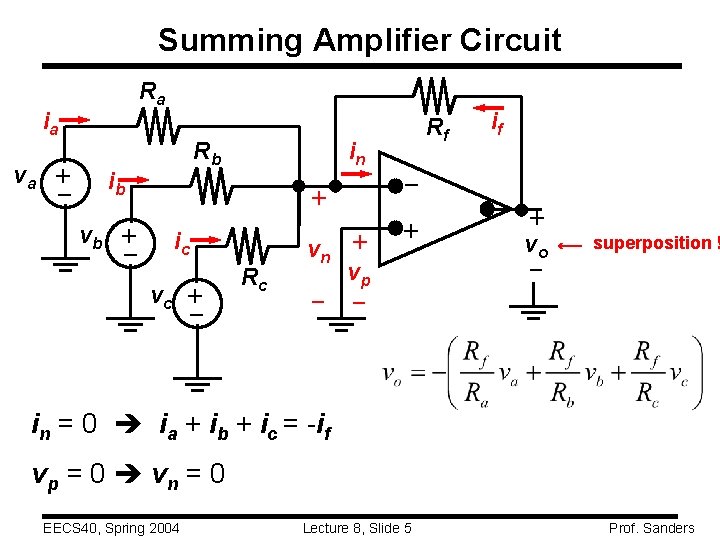
Summing Amplifier Circuit Ra ib + – + ic vc – + vb in Rc vn + vp – – + va Rb Rf if – ia + vo – superposition ! in = 0 ia + ib + ic = -if vp = 0 vn = 0 EECS 40, Spring 2004 Lecture 8, Slide 5 Prof. Sanders

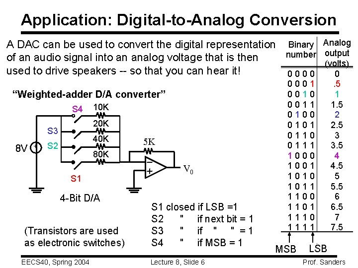
Application: Digital-to-Analog Conversion A DAC can be used to convert the digital representation Binary Analog number output of an audio signal into an analog voltage that is then (volts) used to drive speakers -- so that you can hear it! 0000 0 “Weighted-adder D/A converter” S 4 20 K 40 K S 2 80 K +- S 1 4 -Bit D/A (Transistors are used as electronic switches) EECS 40, Spring 2004 5 K + + S 3 8 V 10 K V 0 S 1 closed if LSB =1 S 2 " if next bit = 1 S 3 " if " " = 1 S 4 " if MSB = 1 Lecture 8, Slide 6 0001 0010 0011 0100 0101 0110 0111 1000 1001 1010 1011 1100 1101 1110 1111 MSB . 5 1 1. 5 2 2. 5 3 3. 5 4 4. 5 5 5. 5 6 6. 5 7 7. 5 LSB Prof. Sanders

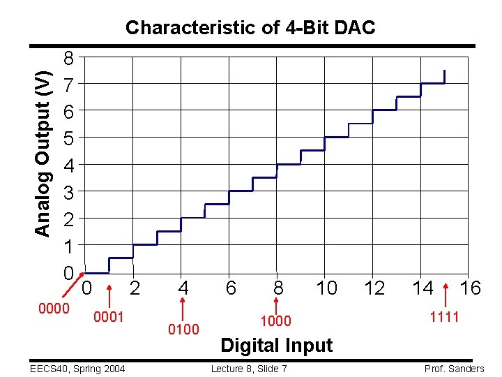
Analog Output (V) Characteristic of 4 -Bit DAC 8 7 6 5 4 3 2 1 0 0000 0 2 0001 EECS 40, Spring 2004 4 0100 6 8 10 1000 12 14 16 1111 Digital Input Lecture 8, Slide 7 Prof. Sanders

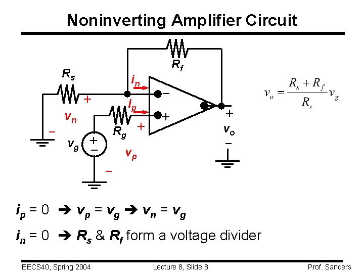
Noninverting Amplifier Circuit + vn vg Rg + – ip + in – Rs Rf vp + vo – – i p = 0 vp = vg vn = vg in = 0 Rs & Rf form a voltage divider EECS 40, Spring 2004 Lecture 8, Slide 8 Prof. Sanders

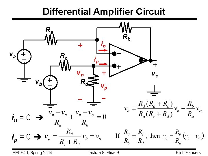
Differential Amplifier Circuit Ra in – + vb ip vn Rd – + + – + Rc – + va Rb vp + vo – – in = 0 ip = 0 EECS 40, Spring 2004 Lecture 8, Slide 9 Prof. Sanders

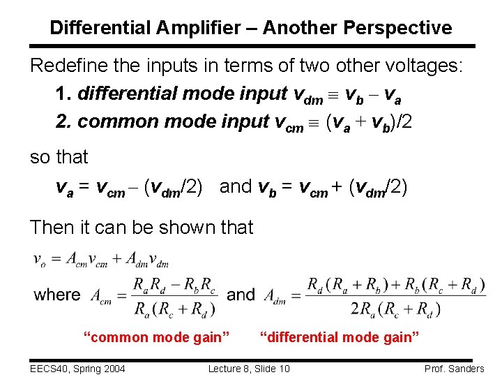
Differential Amplifier – Another Perspective Redefine the inputs in terms of two other voltages: 1. differential mode input vdm vb – va 2. common mode input vcm (va + vb)/2 so that va = vcm – (vdm/2) and vb = vcm + (vdm/2) Then it can be shown that “common mode gain” EECS 40, Spring 2004 “differential mode gain” Lecture 8, Slide 10 Prof. Sanders

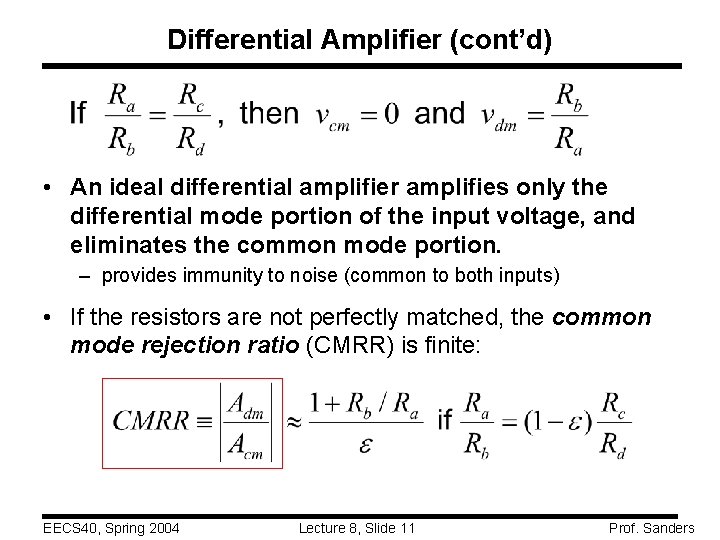
Differential Amplifier (cont’d) • An ideal differential amplifier amplifies only the differential mode portion of the input voltage, and eliminates the common mode portion. – provides immunity to noise (common to both inputs) • If the resistors are not perfectly matched, the common mode rejection ratio (CMRR) is finite: EECS 40, Spring 2004 Lecture 8, Slide 11 Prof. Sanders

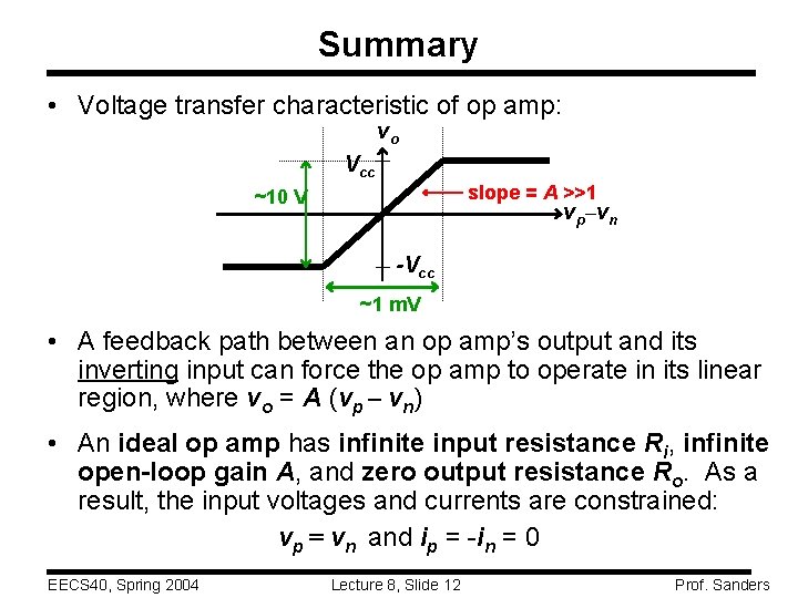
Summary • Voltage transfer characteristic of op amp: vo Vcc slope = A >>1 ~10 V vp–vn -Vcc ~1 m. V • A feedback path between an op amp’s output and its inverting input can force the op amp to operate in its linear region, where vo = A (vp – vn) • An ideal op amp has infinite input resistance Ri, infinite open-loop gain A, and zero output resistance Ro. As a result, the input voltages and currents are constrained: vp = vn and ip = -in = 0 EECS 40, Spring 2004 Lecture 8, Slide 12 Prof. Sanders