Lecture 7 OUTLINE Poissons equation Work function MetalSemiconductor
- Slides: 17

Lecture 7 OUTLINE • Poisson’s equation • Work function • Metal-Semiconductor Contacts – Equilibrium energy band diagrams – Depletion-layer width Reading: Pierret 5. 1. 2, 14. 1 -14. 2; Hu 4. 16

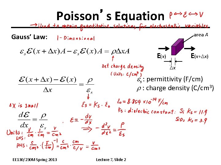
Poisson’s Equation area A Gauss’ Law: E(x) E(x+Dx) Dx s : permittivity (F/cm) : charge density (C/cm 3) EE 130/230 M Spring 2013 Lecture 7, Slide 2

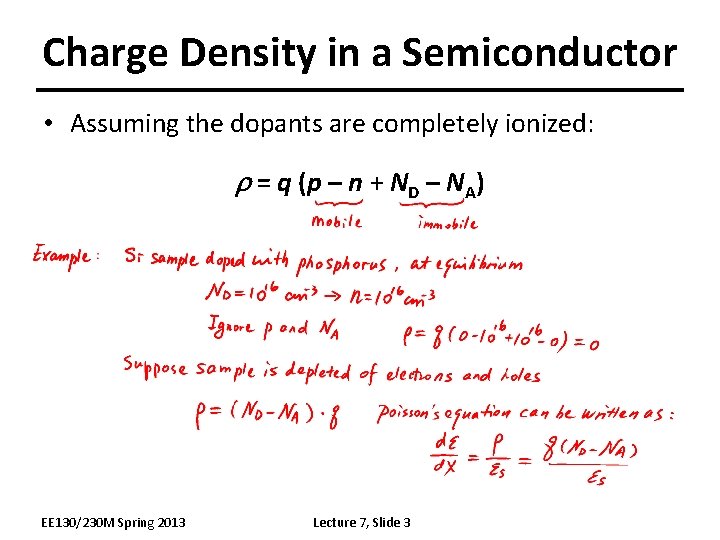
Charge Density in a Semiconductor • Assuming the dopants are completely ionized: r = q (p – n + ND – NA) EE 130/230 M Spring 2013 Lecture 7, Slide 3

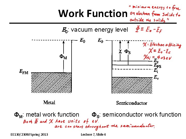
Work Function E 0: vacuum energy level FM: metal work function EE 130/230 M Spring 2013 FS: semiconductor work function Lecture 7, Slide 4

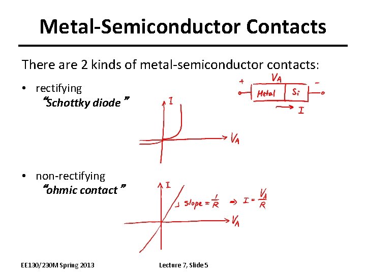
Metal-Semiconductor Contacts There are 2 kinds of metal-semiconductor contacts: • rectifying “Schottky diode” • non-rectifying “ohmic contact” EE 130/230 M Spring 2013 Lecture 7, Slide 5

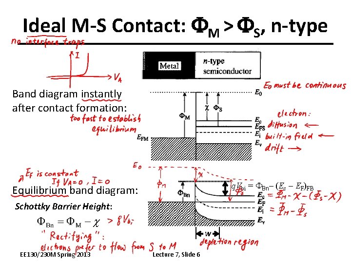
Ideal M-S Contact: FM > FS, n-type Band diagram instantly after contact formation: Equilibrium band diagram: q. Vbi = FBn– (Ec – EF)FB n Schottky Barrier Height: W EE 130/230 M Spring 2013 Lecture 7, Slide 6

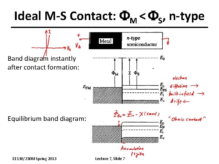
Ideal M-S Contact: FM < FS, n-type Band diagram instantly after contact formation: Equilibrium band diagram: EE 130/230 M Spring 2013 Lecture 7, Slide 7

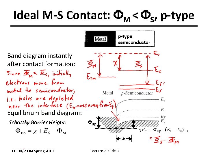
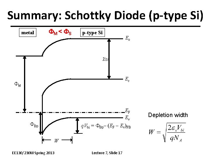
Ideal M-S Contact: FM < FS, p-type semiconductor Band diagram instantly after contact formation: Equilibrium band diagram: Schottky Barrier Height: FBp q. Vbi = FBp– (EF – Ev)FB W EE 130/230 M Spring 2013 Lecture 7, Slide 8

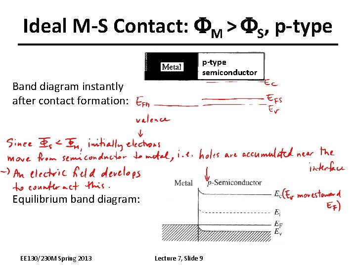
Ideal M-S Contact: FM > FS, p-type semiconductor Band diagram instantly after contact formation: Equilibrium band diagram: EE 130/230 M Spring 2013 Lecture 7, Slide 9

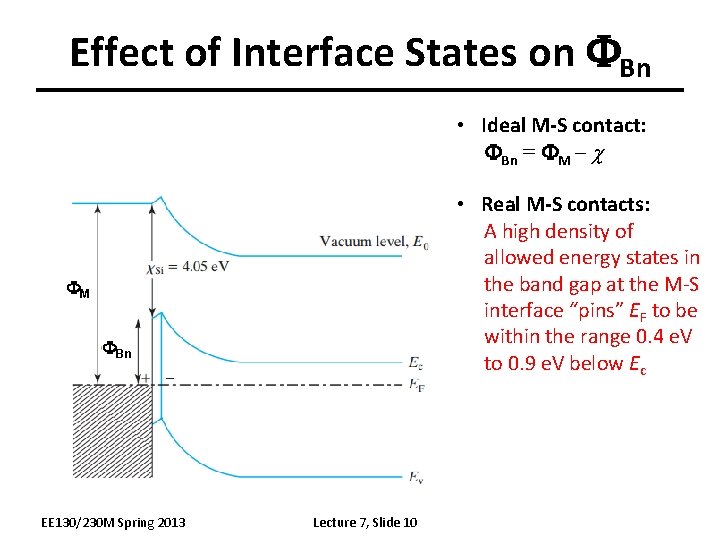
Effect of Interface States on FBn • Ideal M-S contact: FBn = FM – c • Real M-S contacts: A high density of allowed energy states in the band gap at the M-S interface “pins” EF to be within the range 0. 4 e. V to 0. 9 e. V below Ec FM FBn EE 130/230 M Spring 2013 Lecture 7, Slide 10

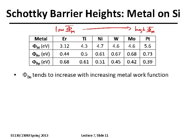
Schottky Barrier Heights: Metal on Si • FBn tends to increase with increasing metal work function EE 130/230 M Spring 2013 Lecture 7, Slide 11

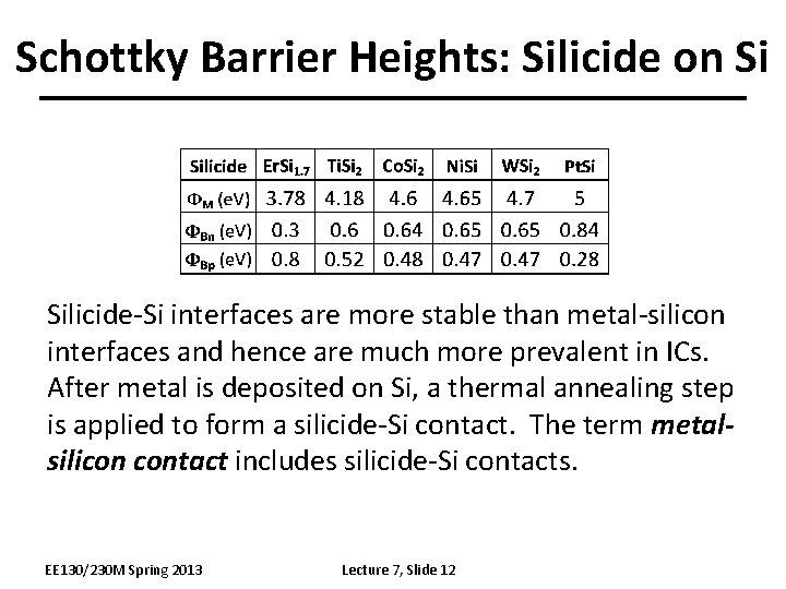
Schottky Barrier Heights: Silicide on Si Silicide-Si interfaces are more stable than metal-silicon interfaces and hence are much more prevalent in ICs. After metal is deposited on Si, a thermal annealing step is applied to form a silicide-Si contact. The term metalsilicon contact includes silicide-Si contacts. EE 130/230 M Spring 2013 Lecture 7, Slide 12

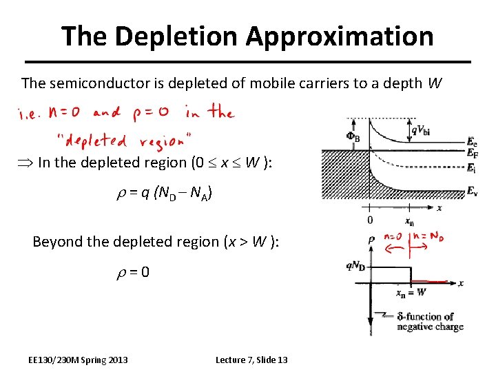
The Depletion Approximation The semiconductor is depleted of mobile carriers to a depth W Þ In the depleted region (0 x W ): = q (ND – NA) Beyond the depleted region (x > W ): =0 EE 130/230 M Spring 2013 Lecture 7, Slide 13

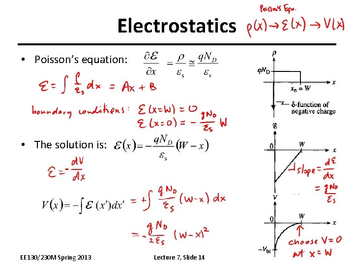
Electrostatics • Poisson’s equation: • The solution is: EE 130/230 M Spring 2013 Lecture 7, Slide 14

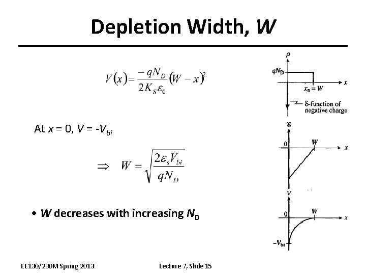
Depletion Width, W At x = 0, V = -Vbi • W decreases with increasing ND EE 130/230 M Spring 2013 Lecture 7, Slide 15

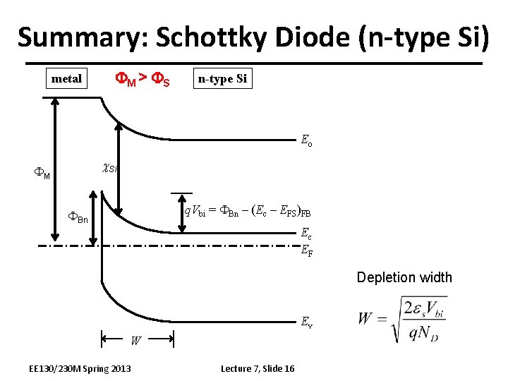
Summary: Schottky Diode (n-type Si) metal FM > FS n-type Si Eo c. Si FM q. Vbi = FBn – (Ec – EFS)FB FBn Ec EF Depletion width Ev W EE 130/230 M Spring 2013 Lecture 7, Slide 16

Summary: Schottky Diode (p-type Si) metal FM < FS p-type Si Eo c. Si Ec FM EF Ev FBp q. Vbi = FBp– (EF – Ev)FB W EE 130/230 M Spring 2013 Lecture 7, Slide 17 Depletion width