LECTURE 7 METALLIZATION OBJECTIVES Ability to explain device

LECTURE 7 METALLIZATION

OBJECTIVES • Ability to explain device application on metallization • Ability to define three most commonly used metals and three different metallization methods • Ability to describe the sputtering process • Ability to explain the purpose of high vacuum in metal deposition processes • Ability to calculate metal thin films measurements

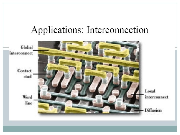
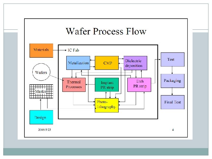
Metallization • Processes that deposit metal thin film on wafer surface. Applications • • Interconnection Gate and electrodes Micro-mirror Fuse

• Low Metal requirements: resistivity to perform high speed devices and low power consumption. • Smooth surface for high resolution patterning process. • Low film stress for good adhesion to underlying substrate. • High resistance to electro migration to achieve high chip reliability. • Cu vs Al. Cu has lower resistivity than Al but technical difficulty such as adhesion, diffusion problems, difficulties with dry etching hampered copper application in IC chip manufacturing.

Resistivity
 q Oxide q Nitride")
Two Types of Thin Film q Dielectric Film (CVD Process) q Oxide q Nitride q Epitaxial silicon q Conducting Film (PVD Process) q Aluminum alloy q Ti, Ti. N q Silicides q Copper (CVD or electroplating) q Tungsten (Metal CVD) q Polysilicon (LPCVD)
 q Gate and electrodes q Polysilicon q")
Conducting Thin Film Applications q Front-End-Of-Line (FEOL) q Gate and electrodes q Polysilicon q Polycide q Back-End-Of-Line (BEOL) q Interconnection q Silicides q Barrier q ARC

q Interconnection q Al-Cu alloy is commonly used material q Deep sub-micron metallization …. Copper ARC - anti reflection coating

q Interconnection q Copper Metallization

q Silicides q To reduce contact resistance of metal / semiconductor interface. q Ti. Si 2, WSi 2 and Co. Si 2 are commonly used materials q Self-aligned-silicide-process (SALICIDE)
 q Ti. N")
q Barrier Layer q To prevent aluminum diffusion into silicon (junction-spiking) q Ti. N is widely used barrier material
 to reduce “notching” during photolithography process. q Ti. N")
q ARC (anti reflective coating) to reduce “notching” during photolithography process. q Ti. N is widely used material

With and without ARC
 Process q PVD works by vaporizing the solid materials, either")
Physical Vapor Deposition (PVD) Process q PVD works by vaporizing the solid materials, either by heating or by sputtering, and re-condensing the vapor on the substrate to form the solid thin film.
 Process q Evaporation q Thermal Evaporation q Electron Beam Evaporation")
Physical Vapor Deposition (PVD) Process q Evaporation q Thermal Evaporation q Electron Beam Evaporation q Sputtering q Simple DC Sputtering q DC Magnetron Sputtering q DC Triode q RF Diode q RF Triode q RF / DC magnetron

Sputtering = ejecting material from a "target" that is a source onto a "substrate" such as a silicon wafer

DMT 242 Wafer Fabrication Thermal Evaporation q In the early years of IC manufacturing, thermal evaporation was widely used for aluminum deposition. q Aluminum is relatively easy to vaporized due to low melting point (6600 C). Mnorhafiz 2011
 – minimize")
q System needs to be under high vacuum (~ 10 -6 Torr) – minimize residue of oxygen and moisture q Flowing large electric current through aluminum charge – resistive heating. q Aluminum starts to vaporized q When aluminum vapor reaches the wafer surface, it re-condenses and forms a thin aluminum film.

q The deposition rate is mainly related to the heating power, which controlled by the electric current. q The higher the current, the higher the deposition rate. q A significant trace amount of sodium Na, low deposition rate and poor step coverage. q Difficult to precisely control the proper proportions for the alloy films such as Al: Si, Al: Cu and Al: Cu: Si. q No longer used for metallization processes in VLSI and ULSI

Electron Beam Evaporation q A beam of electrons, typically with the energy about 10 ke. V and current up to several amperes, is directed at the metal in a water-cooled crucible in vacuum chamber. q This process heats the metal to the evaporation temperature. q IR lamp is used to heat the wafer (improve step coverage).
 q Less sodium")
q Better step coverage (higher surface mobility due to lamp heating) q Less sodium contamination (only part of aluminum charge is vaporized. q Cannot match the quality of sputtering deposition, therefore very rarely used in advanced semiconductor fab.

Sputtering q The most commonly used PVD process for metallization. q Involves energetic ion bombardment, which physically dislodge atoms or molecules from the solid metal surface, and redeposit them on the substrate as thin metal film. q Argon is normally used as sputtering atom because it is inert, relatively heavy, abundant, cost effective.

q When power is applied between two electrodes under low pressure, a free electron is accelerated by the electric field. q When the free electron collides with Ar, another free electron is generated (ionization collision). Ar becomes positively charged. q The free electron repeat this process to generate more free electrons.

q The positively charged Ar ions are accelerated toward a negatively biased cathode, usually called target. q When these energetic argon ions hit the target surface, atoms of the target material are physically removed from the surface by the momentum transfer of the impacting ions and thrown into the vacuum in the form of metal vapor.

q Sputtered-off atoms leave the target and travel inside the vacuum chamber in the form of metal vapor. q Eventually, some of them reach the wafer surface, adsorb and become so-called adatoms. q The adatoms migrate on the surface until they found nucleation sites and rest there. q Other adatoms re-condense around the nucleation sites to form grain. q When the grains grow and meet with other grains, they form a continuous poly-crystalline metal thin film on the wafer surface.

Simple DC Sputtering q The simplest sputtering system. q Wafer is placed on the grounded electrode and the target is the negatively biased electrode, the cathode. q When a high-power DC voltage (several hundred volts) is applied, the argon atoms are ionized by electric field.

q These accelerate and bombard the target, then sputtered-off the target material from the surface.

Sputtering vs. Evaporator Sputtering Evaporator • Purer film • Better uniformity • Single wafer, better process control • Larger size wafer • More impurities • Not very uniform • Batch process (more than one wafer) • Cheaper tool

DC Magnetron Sputtering q The most popular method for PVD metallization process, because it can achieve high deposition rate, good film uniformity, high film quality, and easy process control. q High deposition rate allow single-wafer processing, which has several advantages over batch-processing.

q A rotating magnet is placed on top of metal target. q In a magnetic field, electrons will be constrained near magnetic field line. q This gives electrons more chances for ionization collision. q Therefore, the magnetic field serves to increase plasma density and cause more sputtering near the magnet.

CVD vs PVD q CVD: Chemical reaction on the surface PVD: No chemical reaction i. e. purely physical q CVD: Better step coverage (50 -100%) and gap-fill capability PVD: Poor step coverage (<15%) and gap-fill capability q CVD: Impurities in the film, lower conductivity, hard to deposit alloy. PVD: Purer deposited film, higher conductivity, easy to deposit alloy.

Mnorhafiz 2011

Basic PRE Metallization Process q Burn-in Step q To condition the target before processing production wafers. q Native oxide and defects on the target were removed. q De-gas (Orient/Degas Chamber) q To orient the wafer. q Heat the wafer to drive-out gases and moisture. q Prevent out-gassing during the deposition process

Titanium Deposition Process q Normally deposited as welding layer prior to aluminum alloy deposition (reduce contact resistance) q Titanium can trap oxygen and prevent it from bonding with aluminum to form high resistivity aluminum oxide. q To produce larger grain size, wafer is normally heated to 350 0 C. q Collimated chamber is normally used in deep submicron IC fabrication to achieve better titanium step coverage.

q Collimator allows metal atoms to move in mainly in vertical direction q Significantly improve bottom step coverage

Titanium Nitride Deposition Process q Ti. N is widely used as ARC, glue and barrier layers. q The deposition normally uses a reactive sputtering process. q When nitrogen flows with argon into the process chamber, some nitrogen molecules dissociate as a result of ionization collision. q Free nitrogen radicals are very reactive. They can react with sputtered Ti atoms to form Ti. N and deposit it on the wafer surface. q They can also react with Ti target to form a thin Ti. N layer on the target surface. q Argon bombardment could dislodge Ti. N from the target surface, redeposited on the wafer surface.
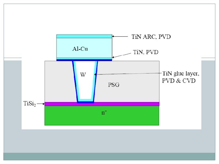

Al-Cu alloy Deposition Process q Needs an ultrahigh baseline vacuum to achieve low film resistivity. q Standard process q Depositing aluminum alloy over tungsten plug, after Ti and Ti. N wetting layer. q Normally deposited at 200 C, to achieve smaller grain size for better line patterned etch.

Metal Thin Film Measurement q Thickness Measurement q Reflectivity q Sheet Resistance q Deposition Rate q Film Stress q Process Uniformity

Thickness Measurement q Metal films such as aluminum, Ti. N and copper are solid films; therefore, optical-based technique such as reflecto-spectrometry cannot be used. q A destructive process is normally required to precisely measure the actual film thickness.
 q SEM / TEM")
Equipments for characterization of metal: q Step height measurement (profilometer) q SEM / TEM q Four point probe – indirect measurement

A diamond stylus is moved vertically in contact with a sample and then moved laterally across the sample for a specified distance and specified contact force. A profilometer can measure small surface variations in vertical stylus displacement as a function of position. A typical profilometer can measure small vertical features ranging in height from 10 nanometres to 1 millimetre. Profilometer
 is a type of electron microscope that produces")
A scanning electron microscope (SEM) is a type of electron microscope that produces images of a sample by scanning it with a focused beam of electrons. The electrons interact with electrons in the sample, producing various signals that can be detected and that contain information about the sample's surface topography and composition. Scanning Electron Microscopy

Comparison SEM and TEM SEM TEM based on scattered electrons based on transmitted electrons produced the image of the sample after the microscope collects and counts the scattered electrons are directly pointed toward the sample. provides a three-dimensional a two-dimensional picture SEM focuses on the sample’s surface and its composition seeks to see what is inside or beyond the surface

Four Point probe Probeis to measure the The purpose of the 4 -point resistivity of any semiconductor material. It can measure either bulk or thin film specimen, each of which consists of a different expression.

Sheet Resistance Measurement q Most important characteristics of conducting film. q Widely used to rapidly monitor the deposition process uniformity by indirectly measure the film thickness. q Four Point Probe is commonly used measurement tool

Deposition Rate

Film Stress Measurement q Stress is due to the mismatch between different materials q Compressive stress causes hillock, short between metal q Tensile stress causes crack, metal open, peel off q Two types of measurement q Contact – profilometer q Non-contact – capacitance measurement

SUMMARY

Q&A
- Slides: 52