Lecture 6 SolidState Diodes and Diode Circuits 1
- Slides: 24

Lecture 6 Solid-State Diodes and Diode Circuits 1

Goals • Understand diode structure and basic layout • Explore various diode models including the mathematical model, the ideal diode model, and the constant voltage drop model • Define regions of operation of the diode (forward, reverse bias, and reverse breakdown) • Apply the various types of models in circuit analysis 2

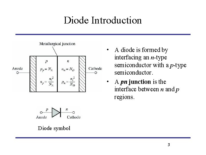
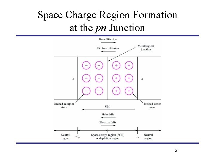
Diode Introduction • A diode is formed by interfacing an n-type semiconductor with a p-type semiconductor. • A pn junction is the interface between n and p regions. Diode symbol 3

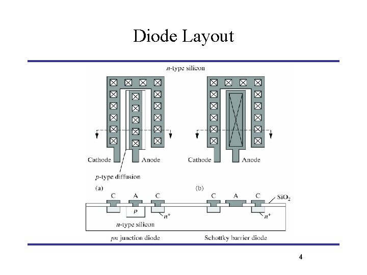
Diode Layout 4

Space Charge Region Formation at the pn Junction 5

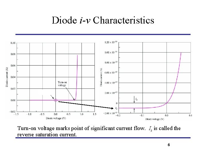
Diode i-v Characteristics Turn-on voltage marks point of significant current flow. Is is called the reverse saturation current. 6

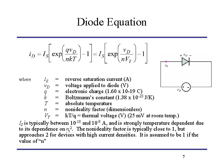
Diode Equation = reverse saturation current (A) v. D = voltage applied to diode (V) q = electronic charge (1. 60 x 10 -19 C) k = Boltzmann’s constant (1. 38 x 10 -23 J/K) T = absolute temperature n = nonideality factor (dimensionless) VT = k. T/q = thermal voltage (V) (25 m. V at room temp. ) IS is typically between 10 -18 and 10 -9 A, and is strongly temperature dependent due to its dependence on ni 2. The nonideality factor is typically close to 1, but approaches 2 for devices with high current densities. It is assumed to be 1 if the value of “n” where IS 7

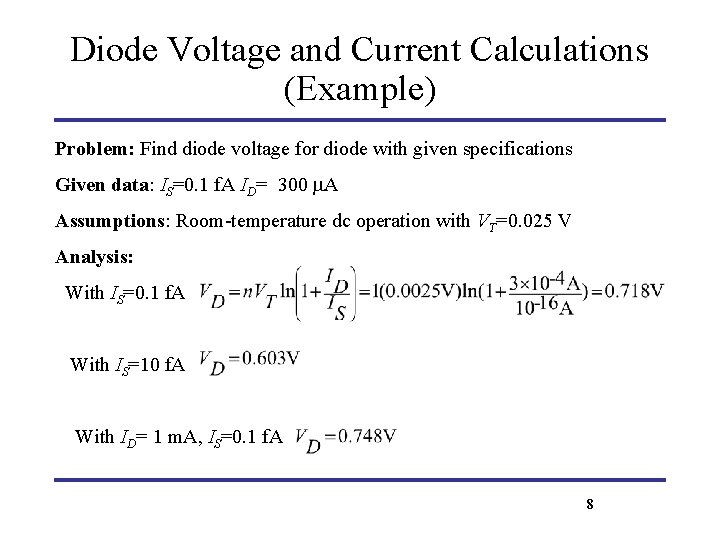
Diode Voltage and Current Calculations (Example) Problem: Find diode voltage for diode with given specifications Given data: IS=0. 1 f. A ID= 300 m. A Assumptions: Room-temperature dc operation with VT=0. 025 V Analysis: With IS=0. 1 f. A With IS=10 f. A With ID= 1 m. A, IS=0. 1 f. A 8

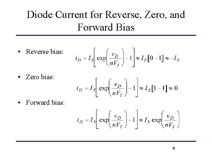
Diode Current for Reverse, Zero, and Forward Bias • Reverse bias: • Zero bias: • Forward bias: 9

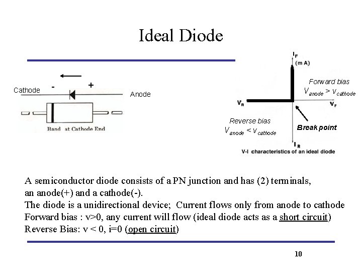
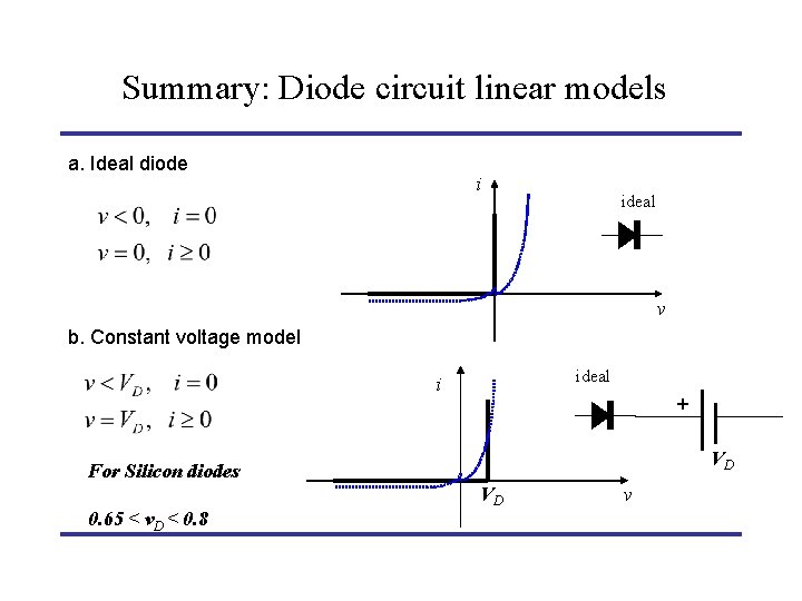
Ideal Diode Cathode - Forward bias + Vanode > vcathode Anode Reverse bias Vanode < vcathode Break point A semiconductor diode consists of a PN junction and has (2) terminals, an anode(+) and a cathode(-). The diode is a unidirectional device; Current flows only from anode to cathode Forward bias : v>0, any current will flow (ideal diode acts as a short circuit) Reverse Bias: v < 0, i=0 (open circuit) 10

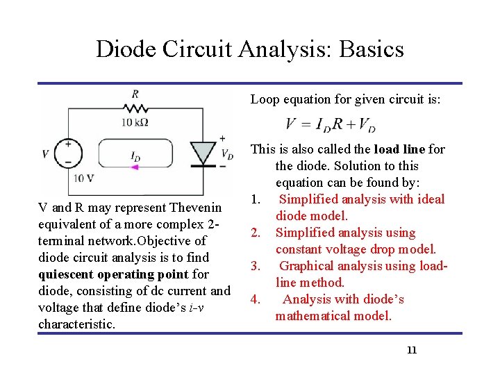
Diode Circuit Analysis: Basics Loop equation for given circuit is: V and R may represent Thevenin equivalent of a more complex 2 terminal network. Objective of diode circuit analysis is to find quiescent operating point for diode, consisting of dc current and voltage that define diode’s i-v characteristic. This is also called the load line for the diode. Solution to this equation can be found by: 1. Simplified analysis with ideal diode model. 2. Simplified analysis using constant voltage drop model. 3. Graphical analysis using loadline method. 4. Analysis with diode’s mathematical model. 11

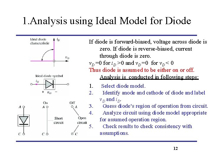
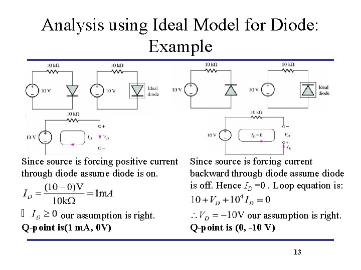
1. Analysis using Ideal Model for Diode If diode is forward-biased, voltage across diode is zero. If diode is reverse-biased, current through diode is zero. v. D =0 for i. D >0 and v. D =0 for v. D < 0 Thus diode is assumed to be either on or off. Analysis is conducted in following steps: 1. Select diode model. 2. Identify anode and cathode of diode and label 3. 4. 5. v. D and i. D. Guess diode’s region of operation from circuit. Analyze circuit using diode model appropriate for assumed operation region. Check results to check consistency with assumptions. 12

Analysis using Ideal Model for Diode: Example Since source is forcing positive current through diode assume diode is on. Since source is forcing current backward through diode assume diode is off. Hence ID =0. Loop equation is: our assumption is right. Q-point is(1 m. A, 0 V) our assumption is right. Q-point is (0, -10 V) 13

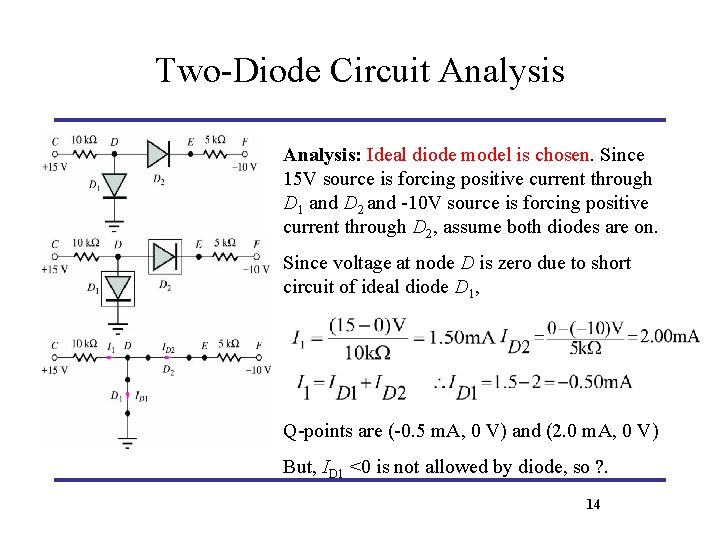
Two-Diode Circuit Analysis: Ideal diode model is chosen. Since 15 V source is forcing positive current through D 1 and D 2 and -10 V source is forcing positive current through D 2, assume both diodes are on. Since voltage at node D is zero due to short circuit of ideal diode D 1, Q-points are (-0. 5 m. A, 0 V) and (2. 0 m. A, 0 V) But, ID 1 <0 is not allowed by diode, so ? . 14

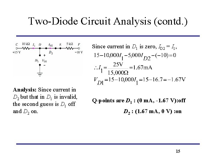
Two-Diode Circuit Analysis (contd. ) Since current in D 1 is zero, ID 2 = I 1, Analysis: Since current in D 2 but that in D 1 is invalid, the second guess is D 1 off and D 2 on. Q-points are D 1 : (0 m. A, -1. 67 V): off D 2 : (1. 67 m. A, 0 V) : on 15

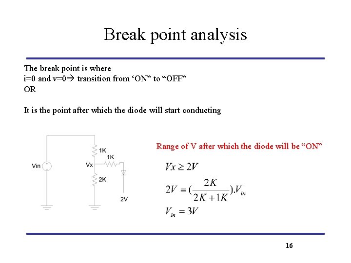
Break point analysis The break point is where i=0 and v=0 transition from ‘ON” to “OFF” OR It is the point after which the diode will start conducting Range of V after which the diode will be “ON” 16

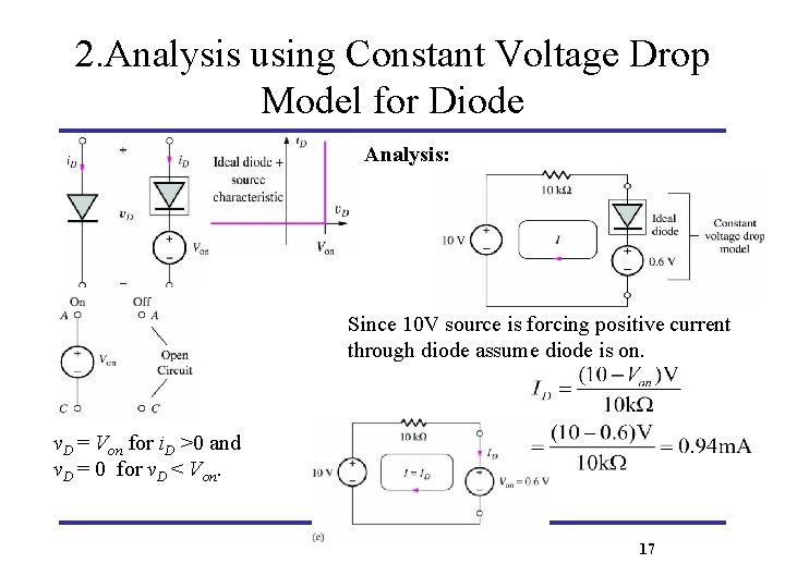
2. Analysis using Constant Voltage Drop Model for Diode Analysis: Since 10 V source is forcing positive current through diode assume diode is on. v. D = Von for i. D >0 and v. D = 0 for v. D < Von. 17

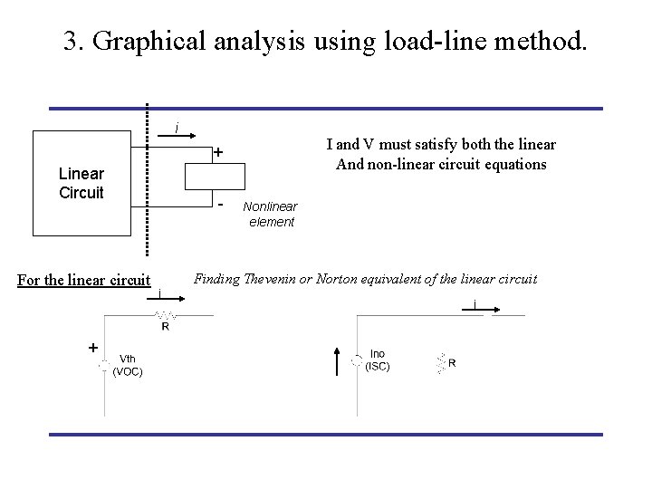
3. Graphical analysis using load-line method. i I and V must satisfy both the linear And non-linear circuit equations + Linear Circuit For the linear circuit + - Nonlinear element Finding Thevenin or Norton equivalent of the linear circuit i i

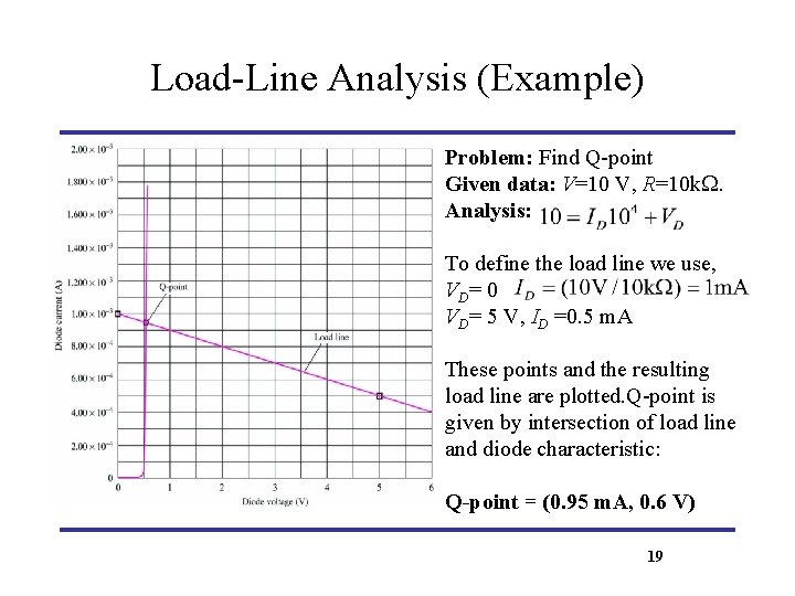
Load-Line Analysis (Example) Problem: Find Q-point Given data: V=10 V, R=10 k. W. Analysis: To define the load line we use, VD= 0 VD= 5 V, ID =0. 5 m. A These points and the resulting load line are plotted. Q-point is given by intersection of load line and diode characteristic: Q-point = (0. 95 m. A, 0. 6 V) 19

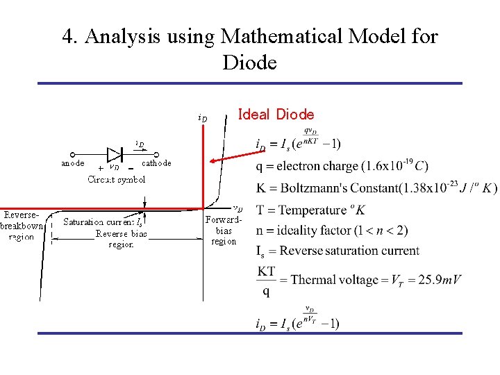
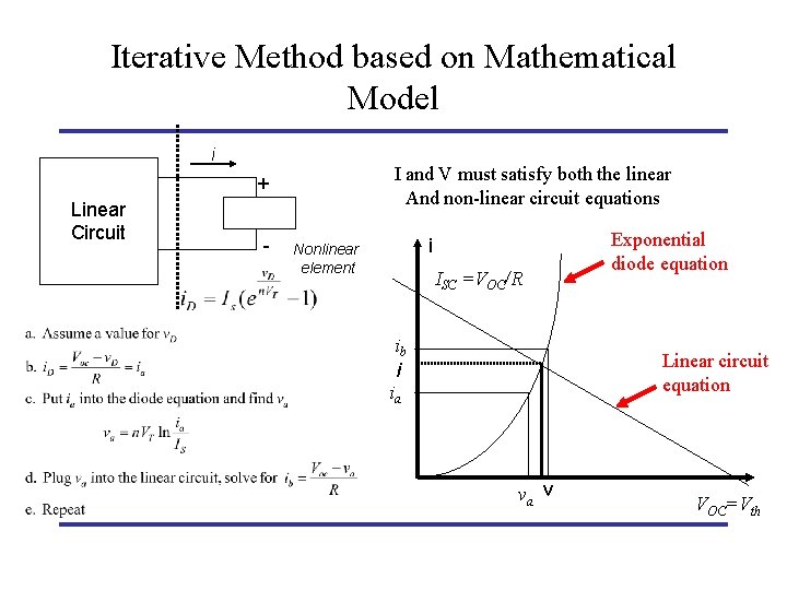
4. Analysis using Mathematical Model for Diode Ideal Diode

Iterative Method based on Mathematical Model i I and V must satisfy both the linear And non-linear circuit equations + Linear Circuit - i Nonlinear element ISC =VOC/R ib i ia Exponential diode equation Linear circuit equation va v VOC=Vth

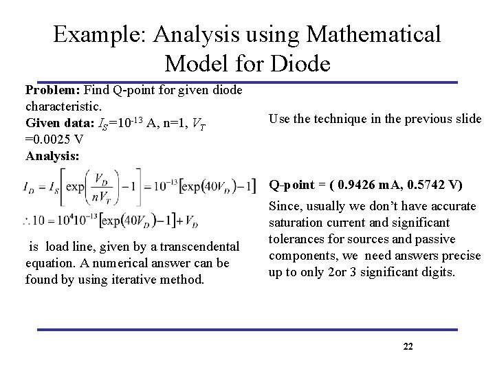
Example: Analysis using Mathematical Model for Diode Problem: Find Q-point for given diode characteristic. Given data: IS =10 -13 A, n=1, VT =0. 0025 V Analysis: Use the technique in the previous slide Q-point = ( 0. 9426 m. A, 0. 5742 V) is load line, given by a transcendental equation. A numerical answer can be found by using iterative method. Since, usually we don’t have accurate saturation current and significant tolerances for sources and passive components, we need answers precise up to only 2 or 3 significant digits. 22

Summary: Diode circuit linear models a. Ideal diode i ideal v b. Constant voltage model ideal i + VD For Silicon diodes 0. 65 < v. D < 0. 8 VD v

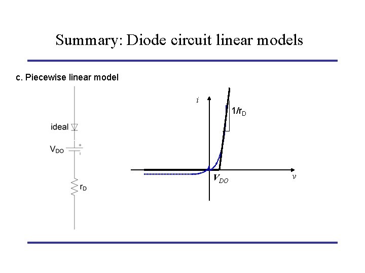
Summary: Diode circuit linear models c. Piecewise linear model i 1/r. D VDO v