Lecture 5 OUTLINE Intrinsic Fermi level Determination of
- Slides: 20

Lecture #5 OUTLINE • Intrinsic Fermi level • Determination of EF • Degenerately doped semiconductor • Carrier properties • Carrier drift Read: Sections 2. 5, 3. 1

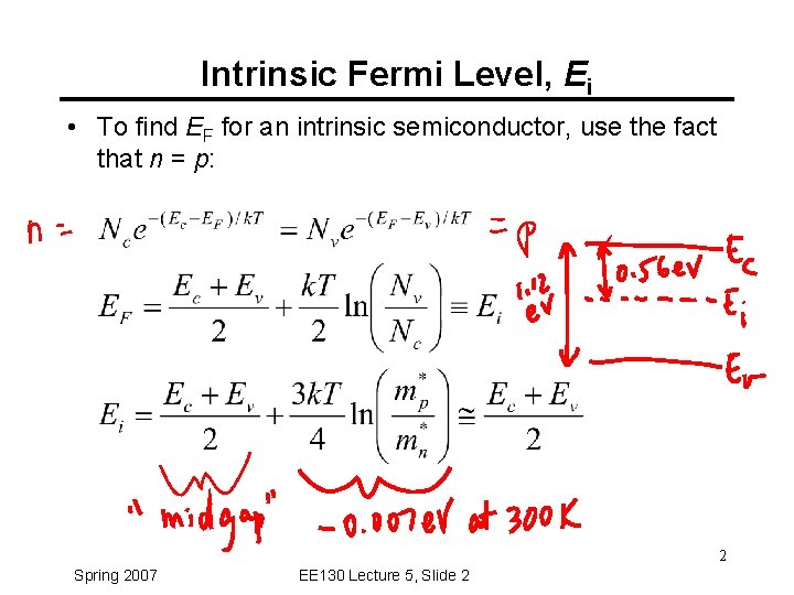
Intrinsic Fermi Level, Ei • To find EF for an intrinsic semiconductor, use the fact that n = p: 2 Spring 2007 EE 130 Lecture 5, Slide 2

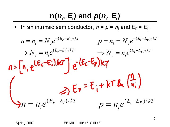
n(ni, Ei) and p(ni, Ei) • In an intrinsic semiconductor, n = p = ni and EF = Ei : 3 Spring 2007 EE 130 Lecture 5, Slide 3

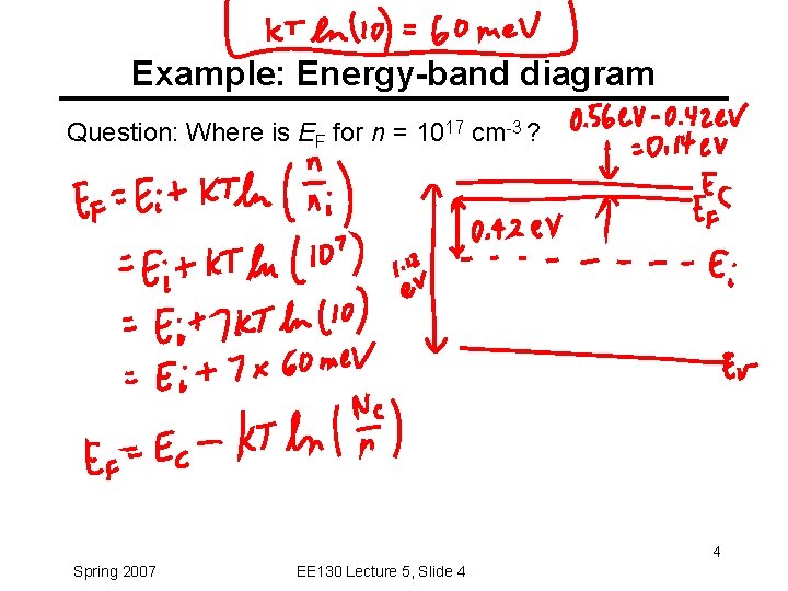
Example: Energy-band diagram Question: Where is EF for n = 1017 cm-3 ? 4 Spring 2007 EE 130 Lecture 5, Slide 4

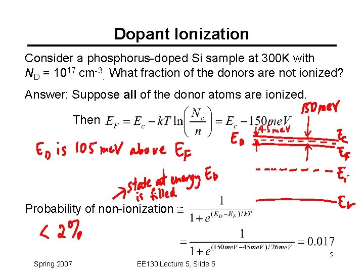
Dopant Ionization Consider a phosphorus-doped Si sample at 300 K with ND = 1017 cm-3. What fraction of the donors are not ionized? Answer: Suppose all of the donor atoms are ionized. Then Probability of non-ionization 5 Spring 2007 EE 130 Lecture 5, Slide 5

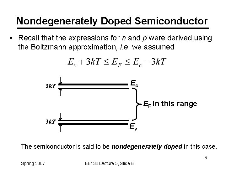
Nondegenerately Doped Semiconductor • Recall that the expressions for n and p were derived using the Boltzmann approximation, i. e. we assumed 3 k. T Ec EF in this range 3 k. T Ev The semiconductor is said to be nondegenerately doped in this case. 6 Spring 2007 EE 130 Lecture 5, Slide 6

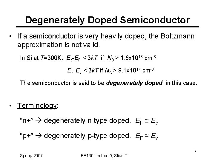
Degenerately Doped Semiconductor • If a semiconductor is very heavily doped, the Boltzmann approximation is not valid. In Si at T=300 K: Ec-EF < 3 k. T if ND > 1. 6 x 1018 cm-3 EF-Ev < 3 k. T if NA > 9. 1 x 1017 cm-3 The semiconductor is said to be degenerately doped in this case. • Terminology: “n+” degenerately n-type doped. EF Ec “p+” degenerately p-type doped. EF Ev 7 Spring 2007 EE 130 Lecture 5, Slide 7

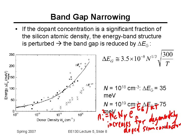
Band Gap Narrowing • If the dopant concentration is a significant fraction of the silicon atomic density, the energy-band structure is perturbed the band gap is reduced by DEG : N = 1018 cm-3: DEG = 35 me. V N = 1019 cm-3: DEG = 75 me. V 8 Spring 2007 EE 130 Lecture 5, Slide 8

Mobile Charge Carriers in Semiconductors • Three primary types of carrier action occur inside a semiconductor: – Drift: charged particle motion under the influence of an electric field. – Diffusion: particle motion due to concentration gradient or temperature gradient. – Recombination-generation (R-G) 9 Spring 2007 EE 130 Lecture 5, Slide 9

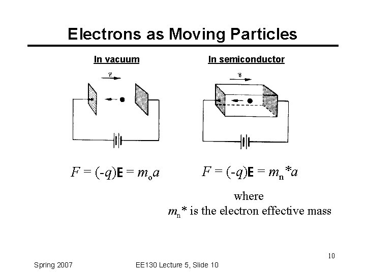
Electrons as Moving Particles In vacuum F = (-q)E = moa In semiconductor F = (-q)E = mn*a where mn* is the electron effective mass 10 Spring 2007 EE 130 Lecture 5, Slide 10

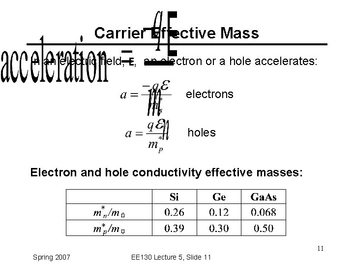
Carrier Effective Mass In an electric field, E, an electron or a hole accelerates: electrons holes Electron and hole conductivity effective masses: * * 11 Spring 2007 EE 130 Lecture 5, Slide 11

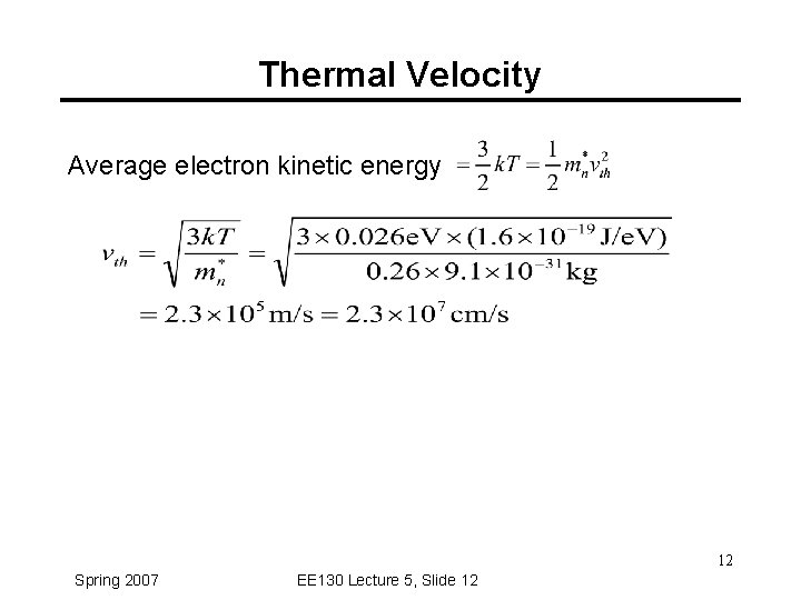
Thermal Velocity Average electron kinetic energy 12 Spring 2007 EE 130 Lecture 5, Slide 12

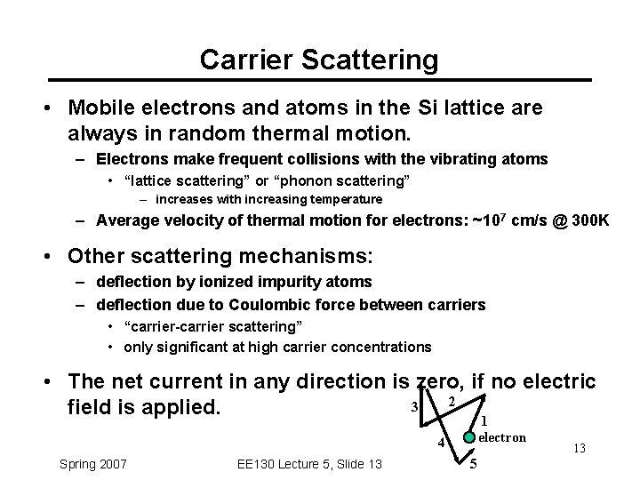
Carrier Scattering • Mobile electrons and atoms in the Si lattice are always in random thermal motion. – Electrons make frequent collisions with the vibrating atoms • “lattice scattering” or “phonon scattering” – increases with increasing temperature – Average velocity of thermal motion for electrons: ~107 cm/s @ 300 K • Other scattering mechanisms: – deflection by ionized impurity atoms – deflection due to Coulombic force between carriers • “carrier-carrier scattering” • only significant at high carrier concentrations • The net current in any direction is zero, if no electric 2 3 field is applied. 1 electron 4 Spring 2007 EE 130 Lecture 5, Slide 13 5 13

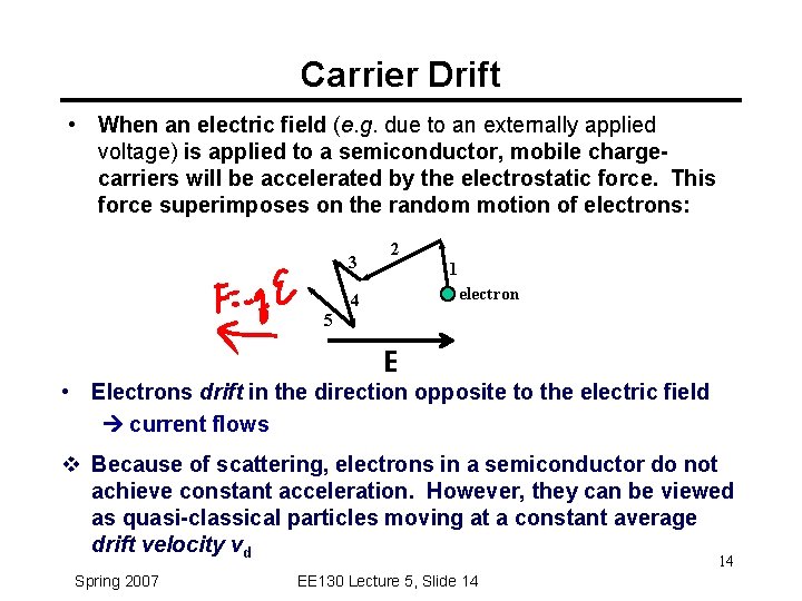
Carrier Drift • When an electric field (e. g. due to an externally applied voltage) is applied to a semiconductor, mobile chargecarriers will be accelerated by the electrostatic force. This force superimposes on the random motion of electrons: 3 2 1 electron 4 5 E • Electrons drift in the direction opposite to the electric field current flows v Because of scattering, electrons in a semiconductor do not achieve constant acceleration. However, they can be viewed as quasi-classical particles moving at a constant average drift velocity vd 14 Spring 2007 EE 130 Lecture 5, Slide 14

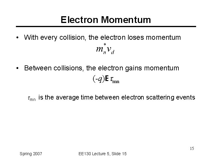
Electron Momentum • With every collision, the electron loses momentum • Between collisions, the electron gains momentum (-q)Etmn is the average time between electron scattering events 15 Spring 2007 EE 130 Lecture 5, Slide 15

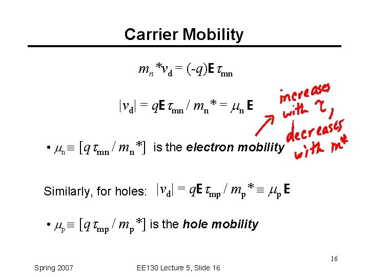
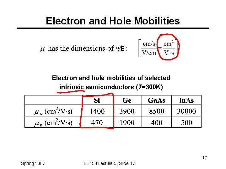
Carrier Mobility mn*vd = (-q)Etmn |vd| = q. Etmn / mn* = n E • n [qtmn / mn*] is the electron mobility Similarly, for holes: |vd| = q. Etmp / mp* p E • p [qtmp / mp*] is the hole mobility 16 Spring 2007 EE 130 Lecture 5, Slide 16

Electron and Hole Mobilities has the dimensions of v/E : Electron and hole mobilities of selected intrinsic semiconductors (T=300 K) 17 Spring 2007 EE 130 Lecture 5, Slide 17

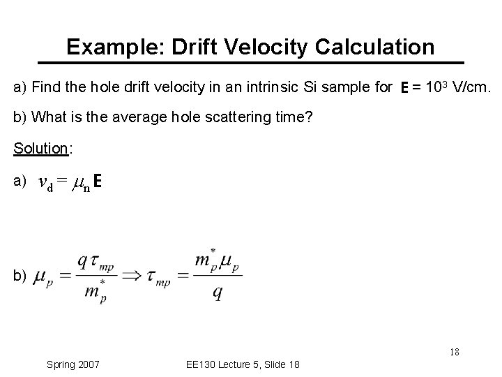
Example: Drift Velocity Calculation a) Find the hole drift velocity in an intrinsic Si sample for E = 103 V/cm. b) What is the average hole scattering time? Solution: a) v d = n E b) 18 Spring 2007 EE 130 Lecture 5, Slide 18

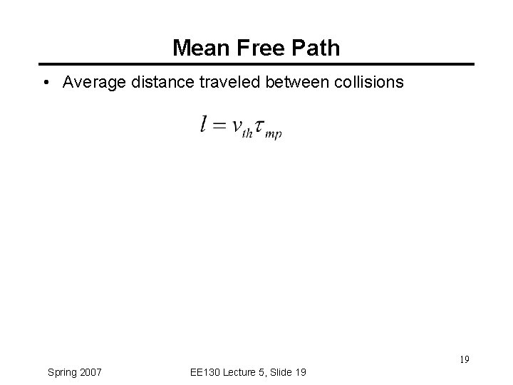
Mean Free Path • Average distance traveled between collisions 19 Spring 2007 EE 130 Lecture 5, Slide 19

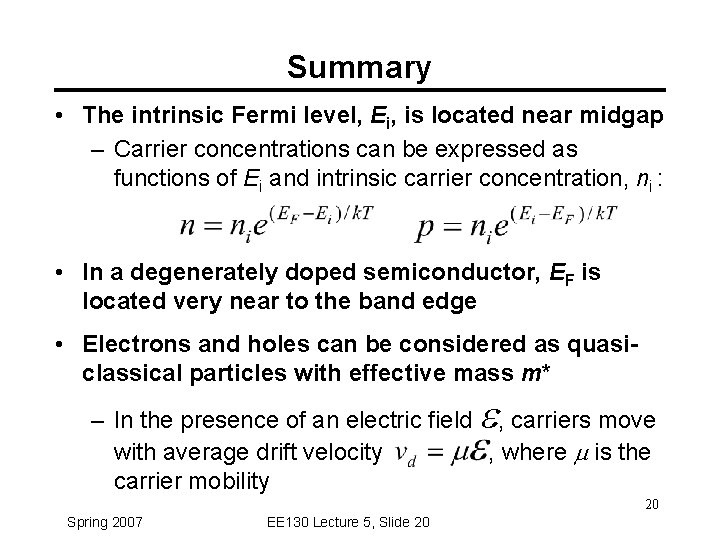
Summary • The intrinsic Fermi level, Ei, is located near midgap – Carrier concentrations can be expressed as functions of Ei and intrinsic carrier concentration, ni : • In a degenerately doped semiconductor, EF is located very near to the band edge • Electrons and holes can be considered as quasiclassical particles with effective mass m* e – In the presence of an electric field , carriers move with average drift velocity , where is the carrier mobility 20 Spring 2007 EE 130 Lecture 5, Slide 20