Lecture 5 Block Diagrams Modes of Operation of
Lecture 5 Block Diagrams Modes of Operation of Block Ciphers

Modes of Operation of Block Ciphers ECE 448 – FPGA and ASIC Design with
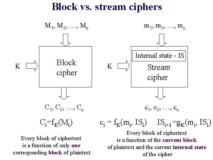
Block vs. stream ciphers M 1, M 2, …, Mn K Block cipher C 1, C 2, …, Cn Ci=f. K(Mi) Every block of ciphertext is a function of only one corresponding block of plaintext m 1, m 2, …, mn Internal state - IS K Stream cipher c 1, c 2, …, cn ci = f. K(mi, ISi) ISi+1=g. K(mi, ISi) Every block of ciphertext is a function of the current block of plaintext and the current internal state of the cipher
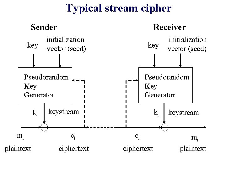
Typical stream cipher Sender key Receiver initialization vector (seed) key Pseudorandom Key Generator ki mi plaintext initialization vector (seed) Pseudorandom Key Generator keystream ki keystream ci ci mi ciphertext plaintext
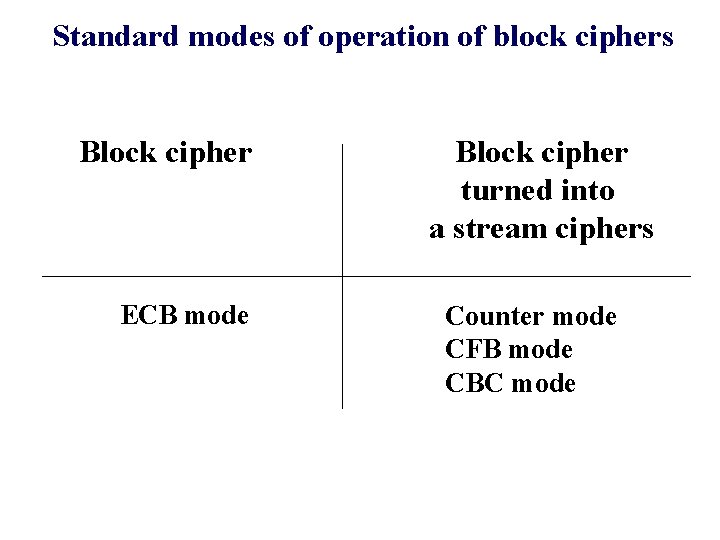
Standard modes of operation of block ciphers Block cipher ECB mode Block cipher turned into a stream ciphers Counter mode CFB mode CBC mode
ECB (Electronic Code. Book) mode
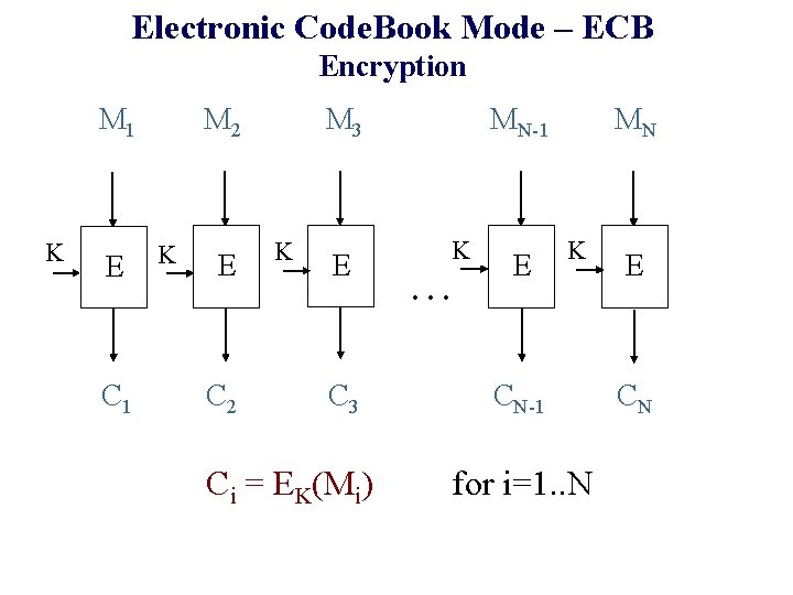
Electronic Code. Book Mode – ECB Encryption M 1 K E C 1 M 3 M 2 K E C 3 Ci = EK(Mi) MN MN-1 K . . . E K CN-1 for i=1. . N E CN
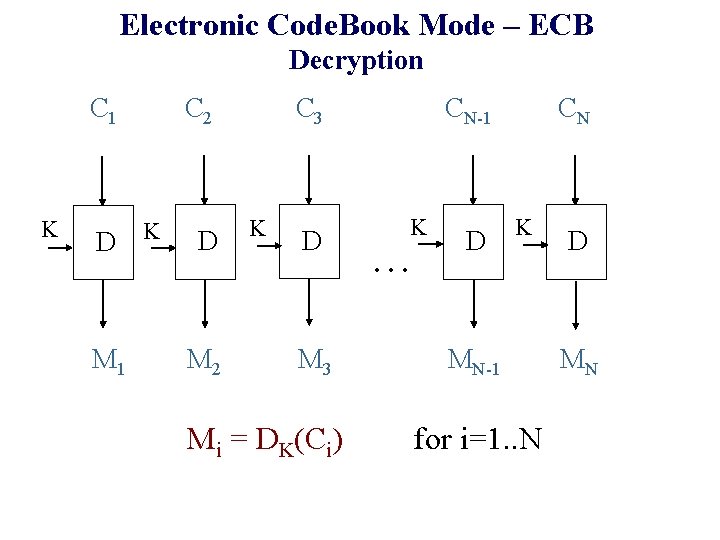
Electronic Code. Book Mode – ECB Decryption C 1 K D M 1 C 3 C 2 K D M 3 Mi = DK(Ci) CN CN-1 K . . . D K MN-1 for i=1. . N D MN
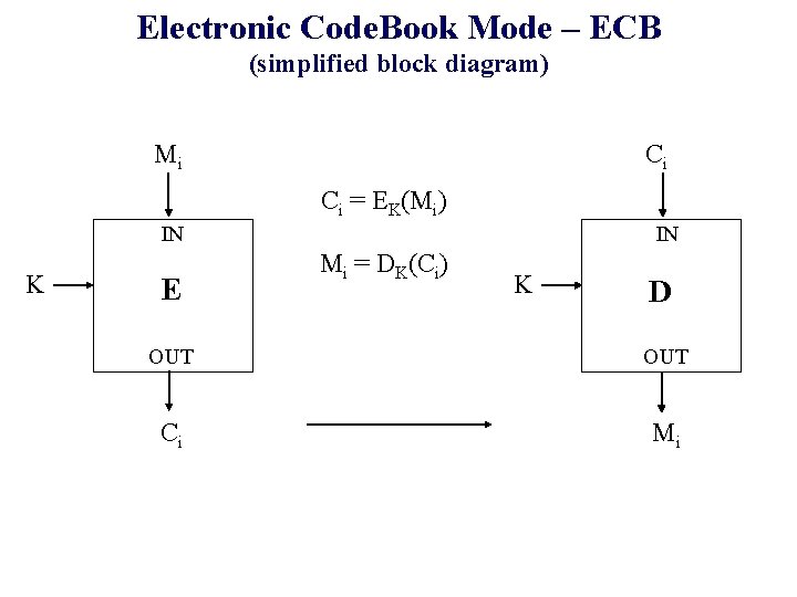
Electronic Code. Book Mode – ECB (simplified block diagram) Mi Ci Ci = EK(Mi) IN K E IN Mi = DK(Ci) K D OUT Ci Mi
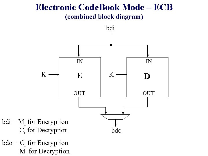
Electronic Code. Book Mode – ECB (combined block diagram) bdi IN K E IN K OUT bdi = Mi for Encryption Ci for Decryption bdo = Ci for Encryption Mi for Decryption D OUT bdo

Counter Mode
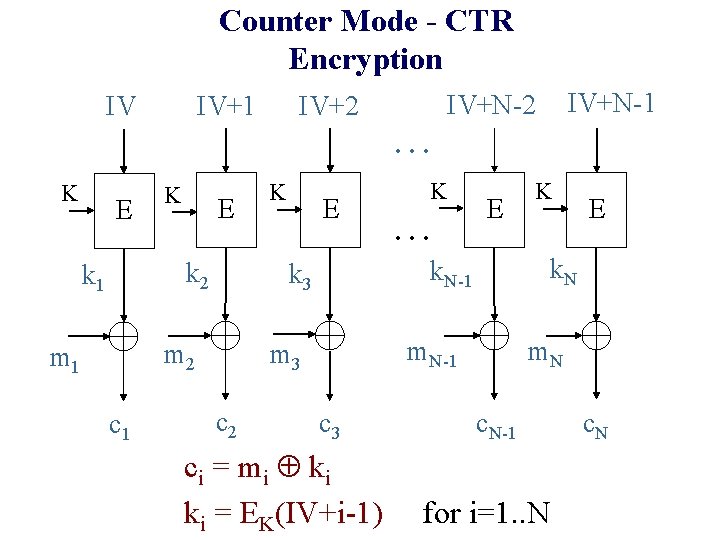
Counter Mode - CTR Encryption IV IV+1 IV+N-2 IV+2. . . K E k 2 k 1 c 1 E . . . E c 3 ci = mi ki ki = EK(IV+i-1) K E k. N m. N-1 m 3 c 2 K k. N-1 k 3 m 2 m 1 K c. N-1 for i=1. . N c. N
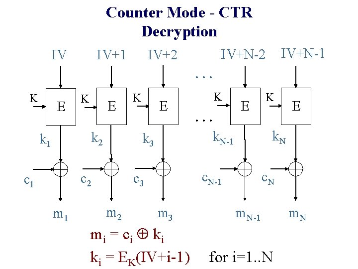
Counter Mode - CTR Decryption IV IV+1 IV+N-2 IV+2. . . K E k 2 k 1 m 1 E . . . E m 3 mi = ci ki ki = EK(IV+i-1) K E k. N c. N-1 c 3 m 2 K k. N-1 k 3 c 2 c 1 K m. N-1 for i=1. . N m. N
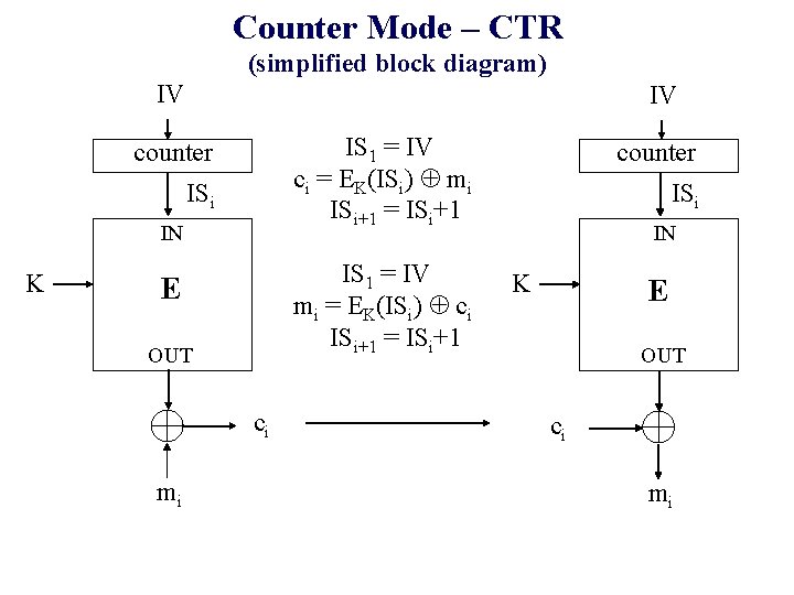
Counter Mode – CTR (simplified block diagram) IV IV IS 1 = IV ci = EK(ISi) mi ISi+1 = ISi+1 counter ISi IN K IS 1 = IV mi = EK(ISi) ci ISi+1 = ISi+1 E OUT ci mi counter ISi IN K E OUT ci mi
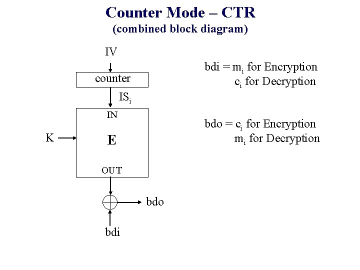
Counter Mode – CTR (combined block diagram) IV bdi = mi for Encryption ci for Decryption counter ISi IN K bdo = ci for Encryption mi for Decryption E OUT bdo bdi

CFB (Cipher Feed. Back) Mode
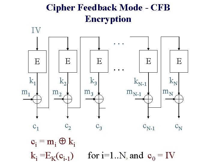
Cipher Feedback Mode - CFB Encryption IV. . . E E k 1 m 1 k 2 m 2 c 1 c 2 ci = mi ki ki =EK(ci-1) E k 3 m 3 c 3 E . . . k. N-1 m. N-1 c. N-1 E k. N m. N c. N for i=1. . N, and c 0 = IV
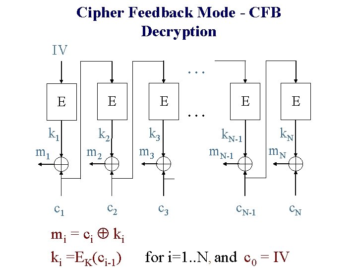
Cipher Feedback Mode - CFB Decryption IV. . . E E k 1 m 1 k 2 m 2 c 1 c 2 mi = ci ki ki =EK(ci-1) E k 3 m 3 c 3 E . . . k. N-1 m. N-1 c. N-1 E k. N m. N c. N for i=1. . N, and c 0 = IV
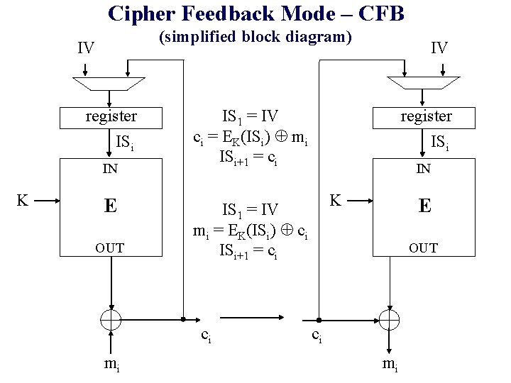
Cipher Feedback Mode – CFB (simplified block diagram) IV register ISi IN K E OUT IS 1 = IV ci = EK(ISi) mi ISi+1 = ci register ISi IN K IS 1 = IV mi = EK(ISi) ci ISi+1 = ci ci mi IV E OUT ci mi
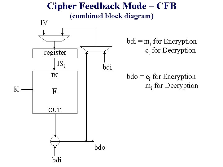
Cipher Feedback Mode – CFB (combined block diagram) IV register ISi bdi = mi for Encryption ci for Decryption bdi IN K bdo = ci for Encryption mi for Decryption E OUT bdo bdi
CBC (Cipher Block Chaining) Mode
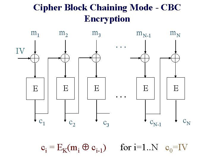
Cipher Block Chaining Mode - CBC Encryption m 1 m 3 m 2 m. N-1 m. N E E . . . IV E E E c 1 c 2 . . . c 3 ci = EK(mi ci-1) c. N-1 c. N for i=1. . N c 0=IV
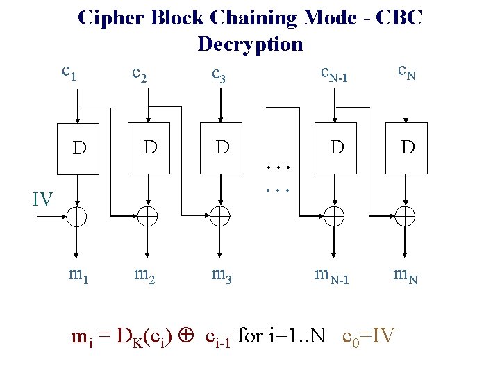
Cipher Block Chaining Mode - CBC Decryption c 1 c 2 c 3 c. N-1 c. N D D m. N-1 m. N D D D m 1 m 2 m 3 IV . . . mi = DK(ci) ci-1 for i=1. . N c 0=IV
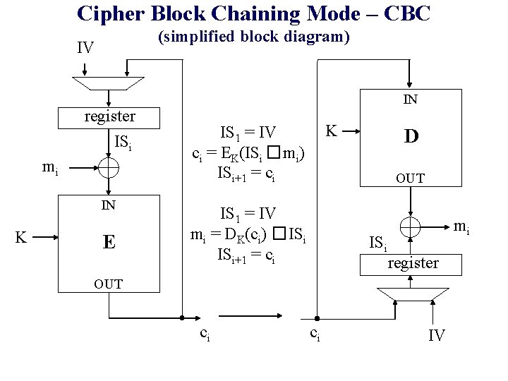
Cipher Block Chaining Mode – CBC (simplified block diagram) IV IN register ISi mi IN K E K IS 1 = IV ci = EK(ISi �mi) ISi+1 = ci D OUT IS 1 = IV mi = DK(ci) �ISi ISi+1 = ci ISi mi register OUT ci ci IV
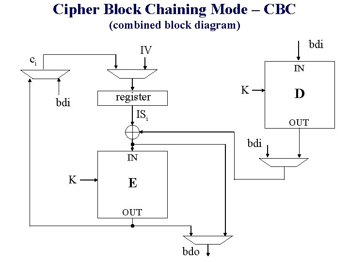
Cipher Block Chaining Mode – CBC (combined block diagram) bdi IV ci IN bdi K register ISi OUT bdi IN K D E OUT bdo

Advanced Encryption Standard (AES) Pseudocode ECE 448 – FPGA and ASIC Design with
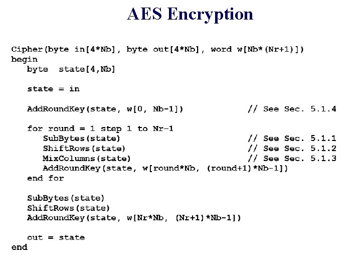
AES Encryption
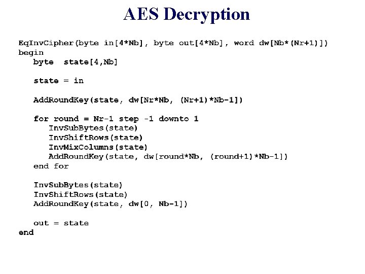
AES Decryption
AES: Symbols, Block Diagrams, Interfaces ECE 448 – FPGA and ASIC Design with
AES_Enc • Encryption Only • Key scheduling done as a part of initialization
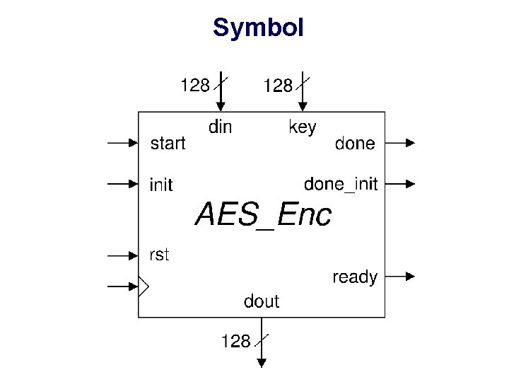
Symbol
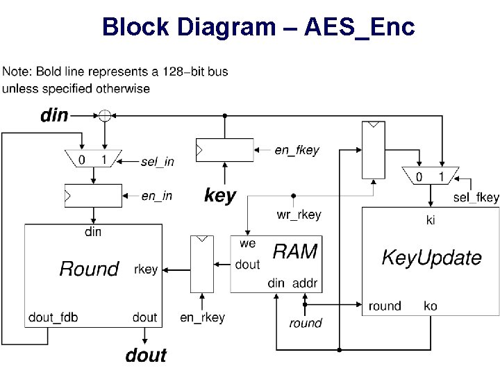
Block Diagram – AES_Enc

Block Diagram – Round
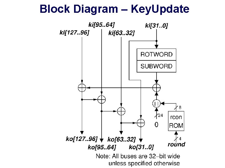
Block Diagram – Key. Update
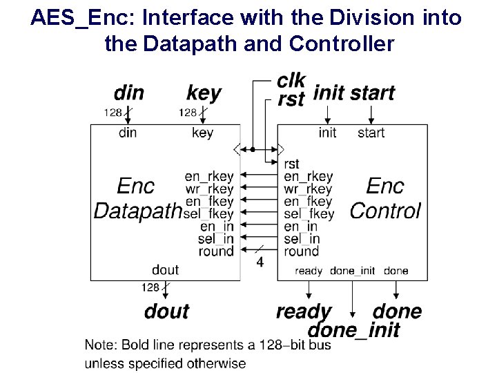
AES_Enc: Interface with the Division into the Datapath and Controller
AES_Enc_KOF • Encryption Only • Key scheduling done On the Fly
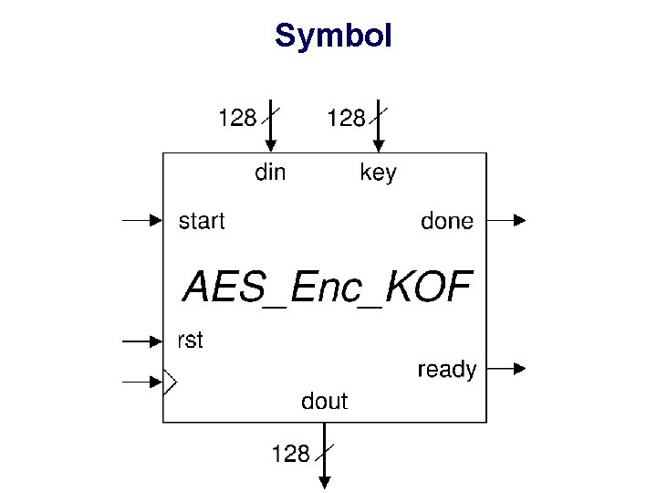
Symbol
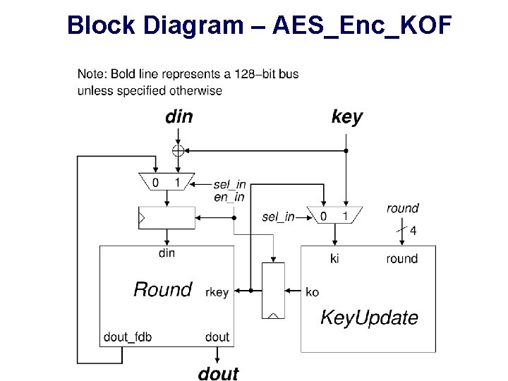
Block Diagram – AES_Enc_KOF
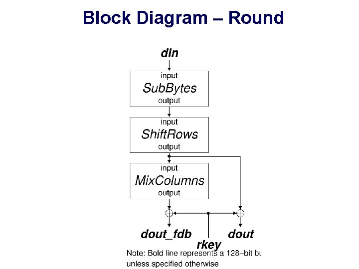
Block Diagram – Round

Block Diagram – Key. Update
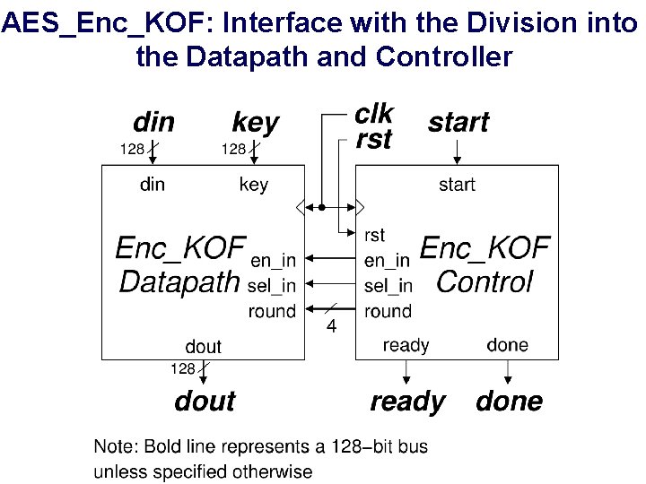
AES_Enc_KOF: Interface with the Division into the Datapath and Controller
AES_Enc. Dec • Encryption and Decryption • Key scheduling done as a part of initialization
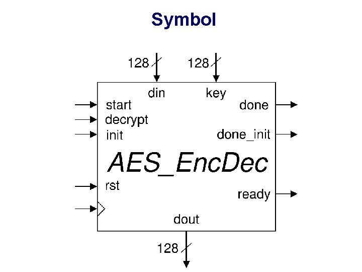
Symbol
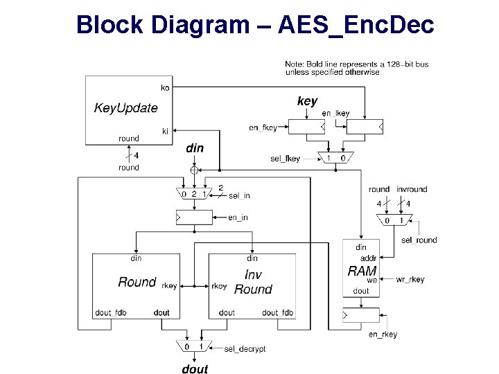
Block Diagram – AES_Enc. Dec

Block Diagram – Round
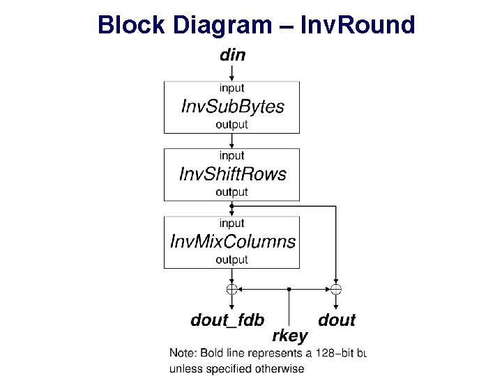
Block Diagram – Inv. Round

Block Diagram – Key. Update
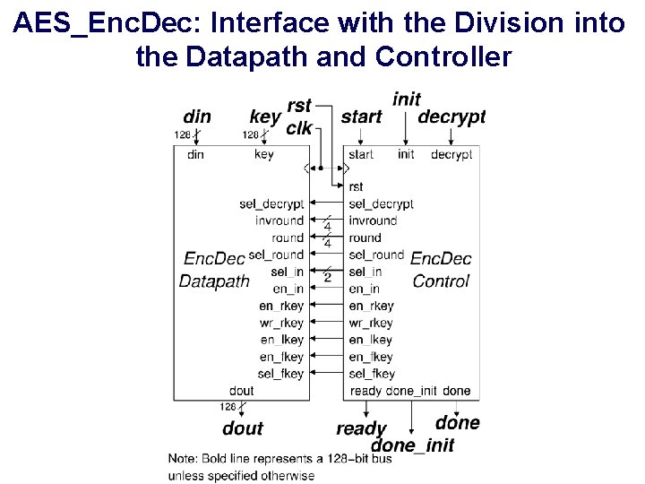
AES_Enc. Dec: Interface with the Division into the Datapath and Controller
Example of a Hierarchical Block Diagram JH hash function ECE 448 – FPGA and ASIC Design with VHDL
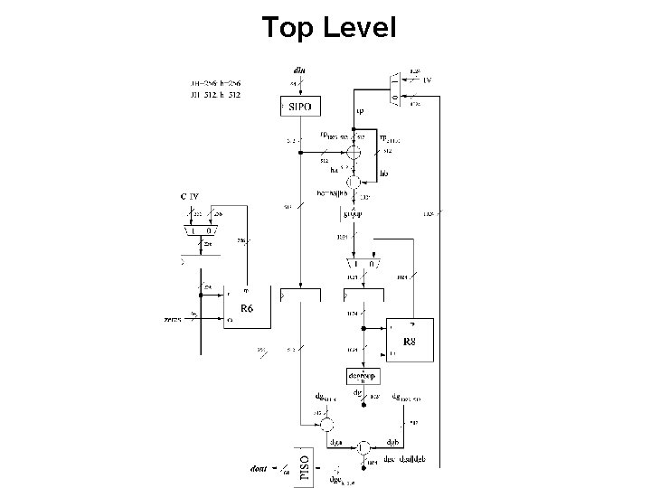
Top Level
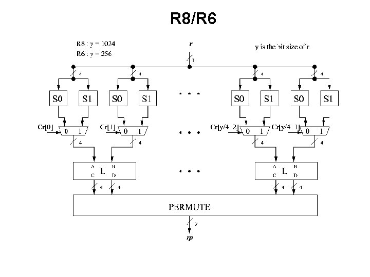
R 8/R 6
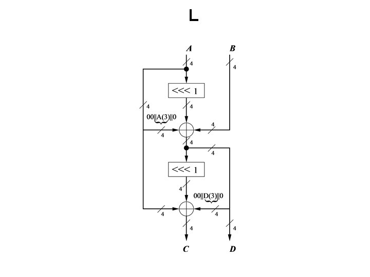
L
Example of a Hierarchical Block Diagram BLAKE hash function ECE 448 – FPGA and ASIC Design with VHDL
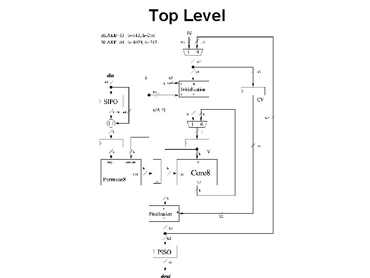
Top Level
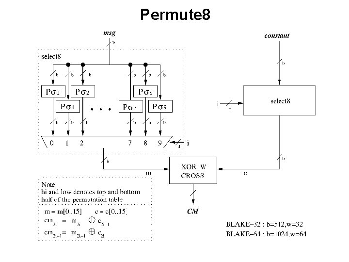
Permute 8
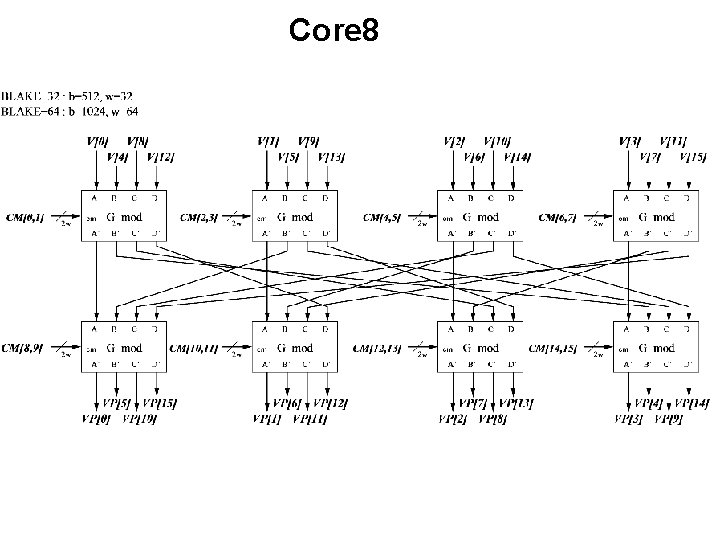
Core 8
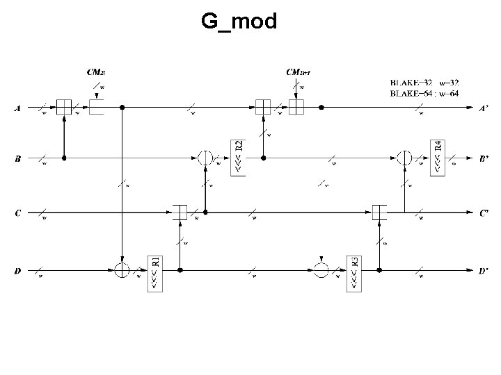
G_mod

Interface of Cipher. Core Datapath ECE 448 – FPGA and ASIC Design with VHDL
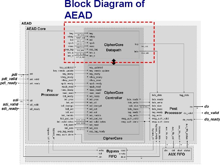
Block Diagram of AEAD 59
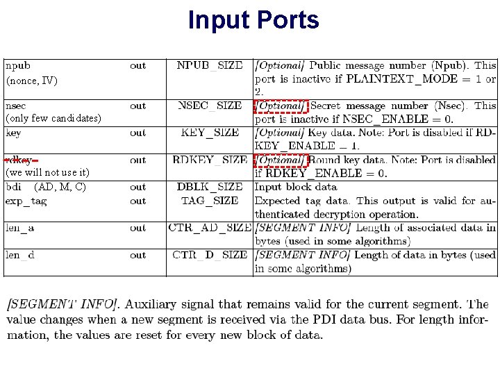
Input Ports (nonce, IV) (only few candidates) (we will not use it) (AD, M, C)

Timeline ECE 448 – FPGA and ASIC Design with VHDL
Project Timeline: Draft Block Diagrams Thursday 10/15, 12 noon: First draft of block diagrams (Blackboard) Thursday 10/15, 1: 00 -4: 30 pm Friday 10/16, 1: 00 -8: 00 pm Discussion of draft block diagrams (30 minutes person, 60 minutes per group, electronic sign-up using Doodle)
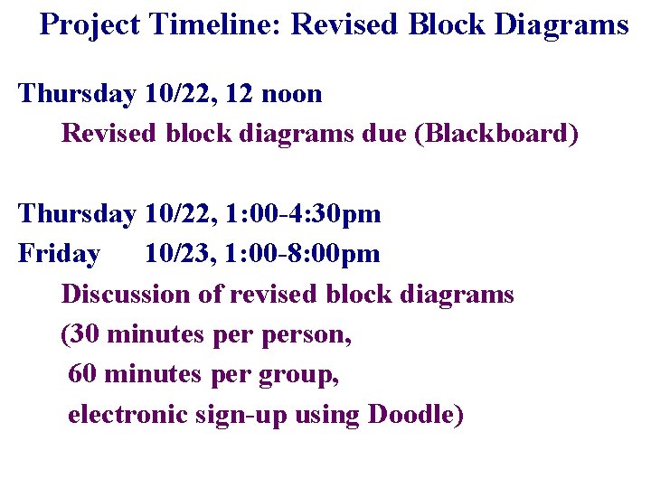
Project Timeline: Revised Block Diagrams Thursday 10/22, 12 noon Revised block diagrams due (Blackboard) Thursday 10/22, 1: 00 -4: 30 pm Friday 10/23, 1: 00 -8: 00 pm Discussion of revised block diagrams (30 minutes person, 60 minutes per group, electronic sign-up using Doodle)
- Slides: 63