Lecture 5 B Block Diagrams HASH Example Structure
Lecture 5 B Block Diagrams HASH Example
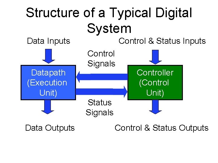
Structure of a Typical Digital System Data Inputs Datapath (Execution Unit) Control & Status Inputs Control Signals Controller (Control Unit) Status Signals Data Outputs Control & Status Outputs
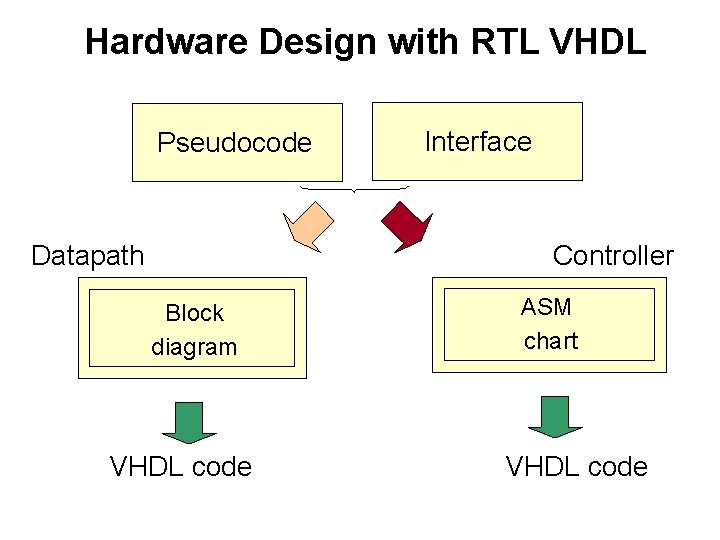
Hardware Design with RTL VHDL Pseudocode Datapath Interface Controller Block diagram VHDL code ASM chart VHDL code
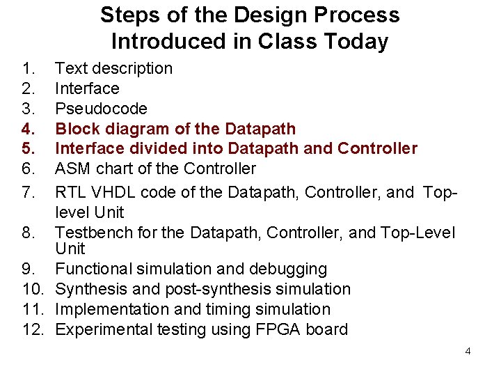
Steps of the Design Process Introduced in Class Today 1. 2. 3. 4. 5. 6. 7. Text description Interface Pseudocode Block diagram of the Datapath Interface divided into Datapath and Controller ASM chart of the Controller RTL VHDL code of the Datapath, Controller, and Toplevel Unit 8. Testbench for the Datapath, Controller, and Top-Level Unit 9. Functional simulation and debugging 10. Synthesis and post-synthesis simulation 11. Implementation and timing simulation 12. Experimental testing using FPGA board 4

Class Exercise 3 HASH FUNCTION
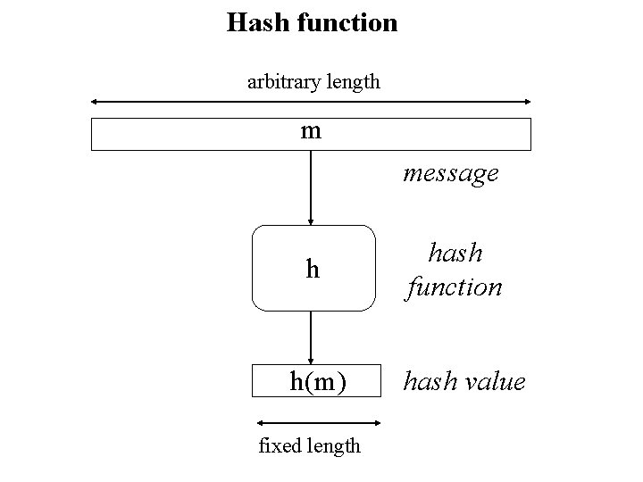
Hash function arbitrary length m message h h(m) fixed length hash function hash value
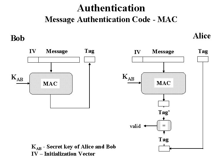
Authentication Message Authentication Code - MAC Alice Bob IV KAB Message Tag MAC IV KAB Message MAC Tag’ valid = Tag KAB - Secret key of Alice and Bob IV – Initialization Vector Tag
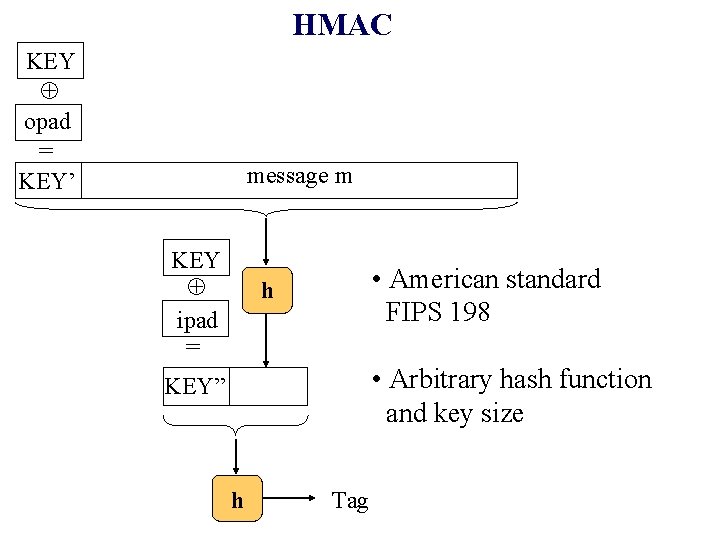
HMAC KEY opad = KEY’ message m KEY ipad = • American standard FIPS 198 h • Arbitrary hash function and key size KEY” h Tag
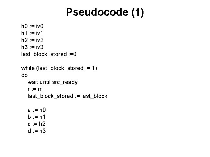
Pseudocode (1) h 0 : = iv 0 h 1 : = iv 1 h 2 : = iv 2 h 3 : = iv 3 last_block_stored : =0 while (last_block_stored != 1) do wait until src_ready r : = m last_block_stored : = last_block a : = h 0 b : = h 1 c : = h 2 d : = h 3
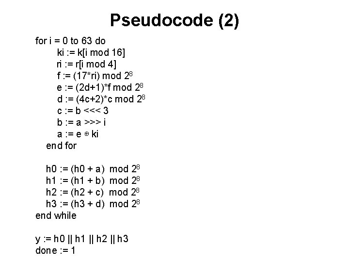
Pseudocode (2) for i = 0 to 63 do ki : = k[i mod 16] ri : = r[i mod 4] f : = (17*ri) mod 28 e : = (2 d+1)*f mod 28 d : = (4 c+2)*c mod 28 c : = b <<< 3 b : = a >>> i a : = e ⊕ ki end for h 0 : = (h 0 + a) h 1 : = (h 1 + b) h 2 : = (h 2 + c) h 3 : = (h 3 + d) end while mod 28 y : = h 0 || h 1 || h 2 || h 3 done : = 1
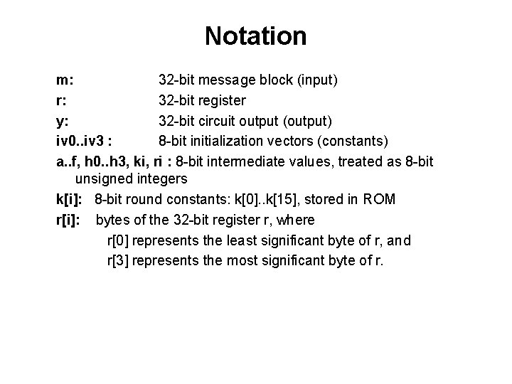
Notation m: 32 -bit message block (input) r: 32 -bit register y: 32 -bit circuit output (output) iv 0. . iv 3 : 8 -bit initialization vectors (constants) a. . f, h 0. . h 3, ki, ri : 8 -bit intermediate values, treated as 8 -bit unsigned integers k[i]: 8 -bit round constants: k[0]. . k[15], stored in ROM r[i]: bytes of the 32 -bit register r, where r[0] represents the least significant byte of r, and r[3] represents the most significant byte of r.
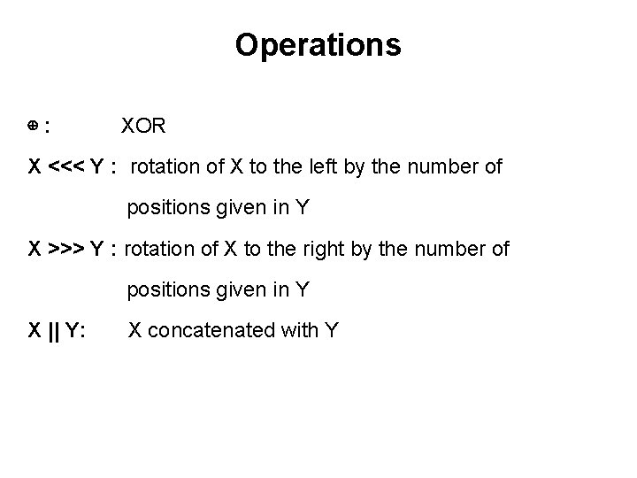
Operations ⊕: XOR X <<< Y : rotation of X to the left by the number of positions given in Y X >>> Y : rotation of X to the right by the number of positions given in Y X || Y: X concatenated with Y
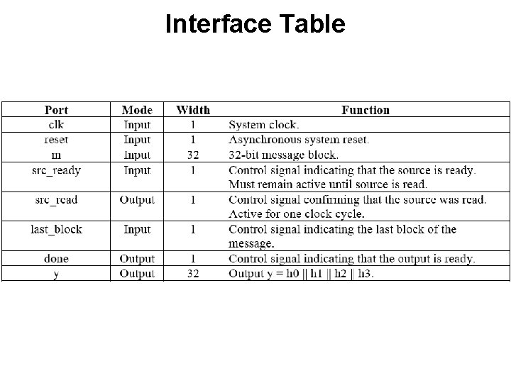
Interface Table
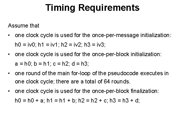
Timing Requirements Assume that • one clock cycle is used for the once-per-message initialization: h 0 = iv 0; h 1 = iv 1; h 2 = iv 2; h 3 = iv 3; • one clock cycle is used for the once-per-block initialization: a = h 0; b = h 1; c = h 2; d = h 3; • one round of the main for-loop of the pseudocode executes in one clock cycle; there a total of 64 rounds. • one clock cycle is used for the once-per-block finalization: h 0 = h 0 + a; h 1 = h 1 + b; h 2 = h 2 + c; h 3 = h 3 + d;
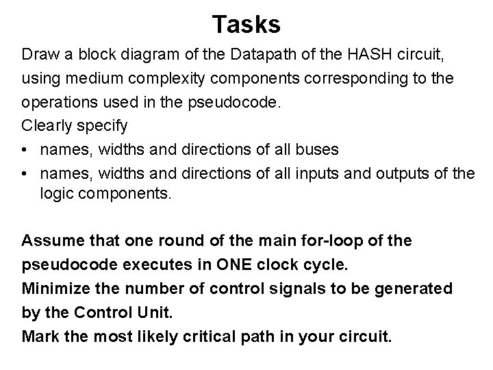
Tasks Draw a block diagram of the Datapath of the HASH circuit, using medium complexity components corresponding to the operations used in the pseudocode. Clearly specify • names, widths and directions of all buses • names, widths and directions of all inputs and outputs of the logic components. Assume that one round of the main for-loop of the pseudocode executes in ONE clock cycle. Minimize the number of control signals to be generated by the Control Unit. Mark the most likely critical path in your circuit.

HASH: Solutions
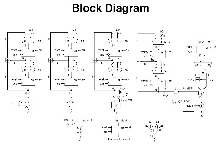
Block Diagram
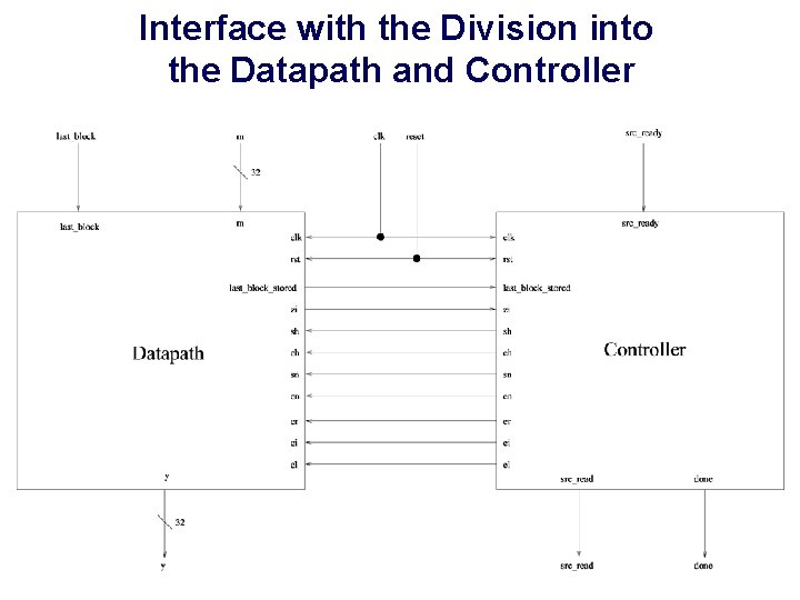
Interface with the Division into the Datapath and Controller
- Slides: 18