Lecture 4 OUTLINE Semiconductor Fundamentals contd Properties of
- Slides: 27

Lecture 4 OUTLINE • Semiconductor Fundamentals (cont’d) – Properties of carriers in semiconductors – Carrier drift • Scattering mechanisms • Drift current – Conductivity and resistivity Reading: Pierret 3. 1; Hu 1. 5, 2. 1 -2. 2

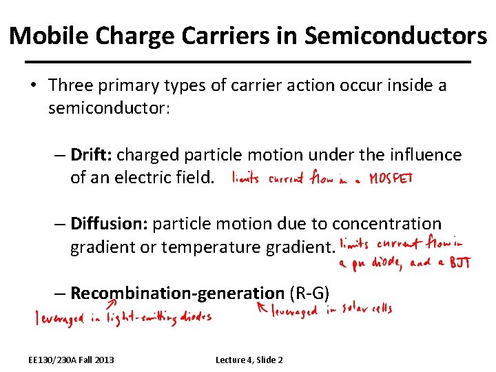
Mobile Charge Carriers in Semiconductors • Three primary types of carrier action occur inside a semiconductor: – Drift: charged particle motion under the influence of an electric field. – Diffusion: particle motion due to concentration gradient or temperature gradient. – Recombination-generation (R-G) EE 130/230 A Fall 2013 Lecture 4, Slide 2

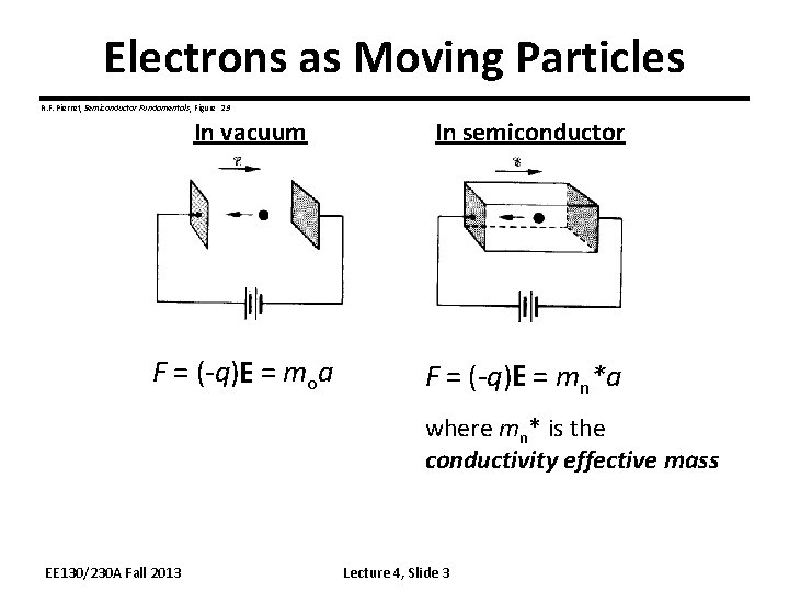
Electrons as Moving Particles R. F. Pierret, Semiconductor Fundamentals, Figure 2. 9 In vacuum In semiconductor F = (-q)E = moa F = (-q)E = mn*a where mn* is the conductivity effective mass EE 130/230 A Fall 2013 Lecture 4, Slide 3

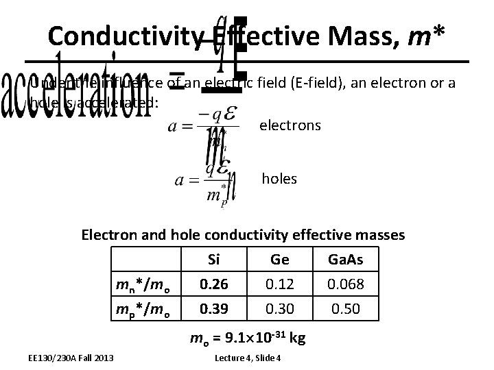
Conductivity Effective Mass, m* Under the influence of an electric field (E-field), an electron or a hole is accelerated: electrons holes Electron and hole conductivity effective masses Si Ge Ga. As mn*/mo 0. 26 0. 12 0. 068 mp*/mo 0. 39 0. 30 0. 50 mo = 9. 1 10 -31 kg EE 130/230 A Fall 2013 Lecture 4, Slide 4

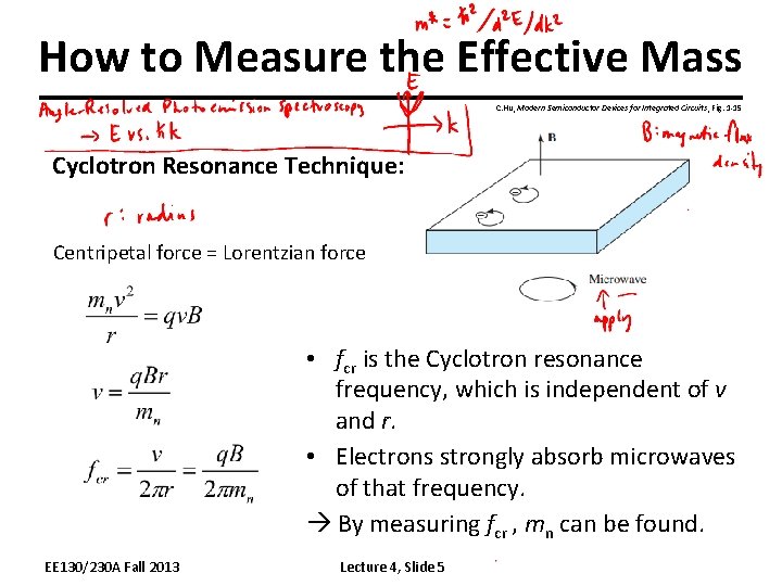
How to Measure the Effective Mass C. Hu, Modern Semiconductor Devices for Integrated Circuits, Fig. 1 -15 Cyclotron Resonance Technique: Centripetal force = Lorentzian force • fcr is the Cyclotron resonance frequency, which is independent of v and r. • Electrons strongly absorb microwaves of that frequency. By measuring fcr , mn can be found. EE 130/230 A Fall 2013 Lecture 4, Slide 5

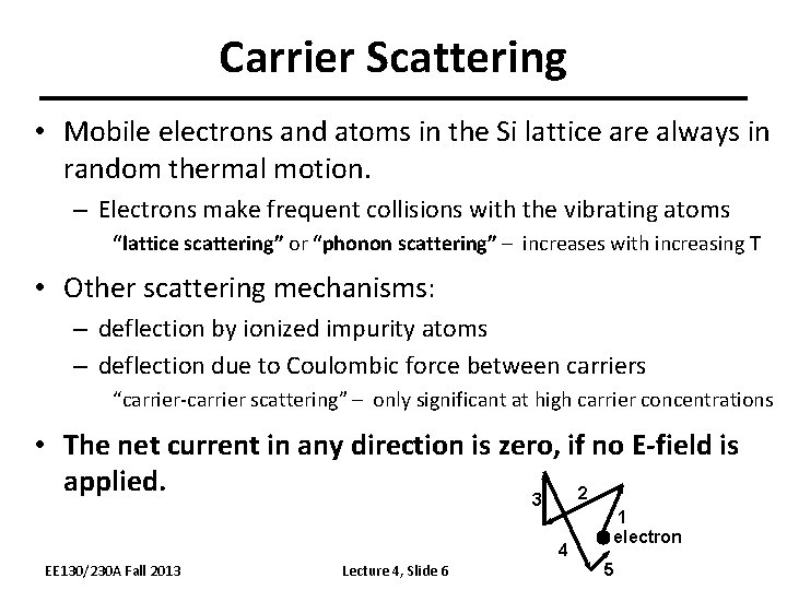
Carrier Scattering • Mobile electrons and atoms in the Si lattice are always in random thermal motion. – Electrons make frequent collisions with the vibrating atoms “lattice scattering” or “phonon scattering” – increases with increasing T • Other scattering mechanisms: – deflection by ionized impurity atoms – deflection due to Coulombic force between carriers “carrier-carrier scattering” – only significant at high carrier concentrations • The net current in any direction is zero, if no E-field is applied. 2 3 4 EE 130/230 A Fall 2013 Lecture 4, Slide 6 1 electron 5

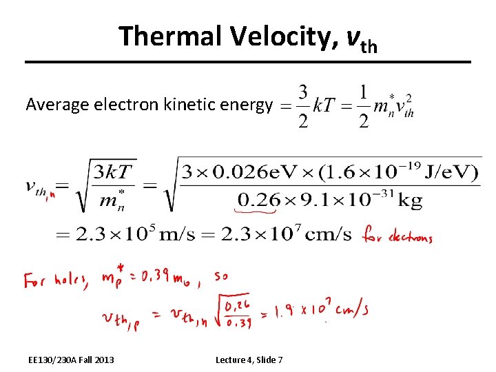
Thermal Velocity, vth Average electron kinetic energy EE 130/230 A Fall 2013 Lecture 4, Slide 7

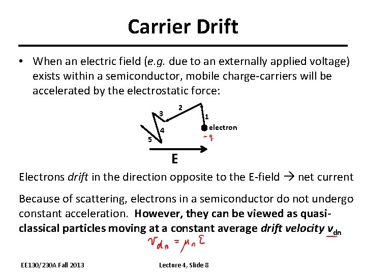
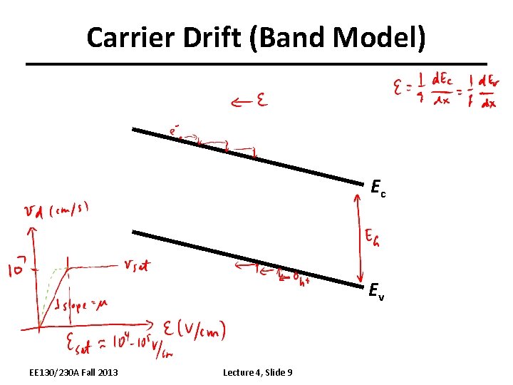
Carrier Drift • When an electric field (e. g. due to an externally applied voltage) exists within a semiconductor, mobile charge-carriers will be accelerated by the electrostatic force: 2 3 5 1 electron 4 E Electrons drift in the direction opposite to the E-field net current Because of scattering, electrons in a semiconductor do not undergo constant acceleration. However, they can be viewed as quasiclassical particles moving at a constant average drift velocity vdn EE 130/230 A Fall 2013 Lecture 4, Slide 8

Carrier Drift (Band Model) Ec Ev EE 130/230 A Fall 2013 Lecture 4, Slide 9

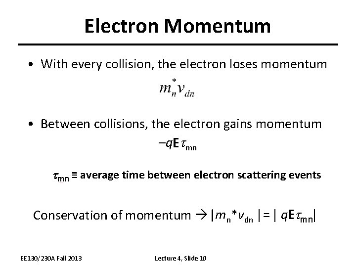
Electron Momentum • With every collision, the electron loses momentum • Between collisions, the electron gains momentum –q. E mn tmn ≡ average time between electron scattering events Conservation of momentum |mn*vdn | = | q. E mn| EE 130/230 A Fall 2013 Lecture 4, Slide 10

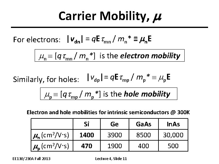
Carrier Mobility, m For electrons: |vdn| = q. E mn / mn* ≡ mn. E n [q mn / mn*] is the electron mobility Similarly, for holes: |vdp|= q. E mp / mp* p. E p [q mp / mp*] is the hole mobility Electron and hole mobilities for intrinsic semiconductors @ 300 K mn (cm 2/V s) mp (cm 2/V s) EE 130/230 A Fall 2013 Si 1400 470 Ge 3900 1900 Lecture 4, Slide 11 Ga. As 8500 400 In. As 30, 000 500

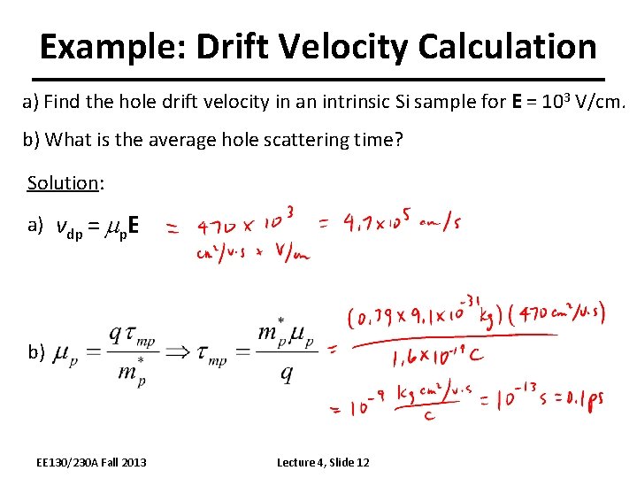
Example: Drift Velocity Calculation a) Find the hole drift velocity in an intrinsic Si sample for E = 103 V/cm. b) What is the average hole scattering time? Solution: a) vdp = p. E b) EE 130/230 A Fall 2013 Lecture 4, Slide 12

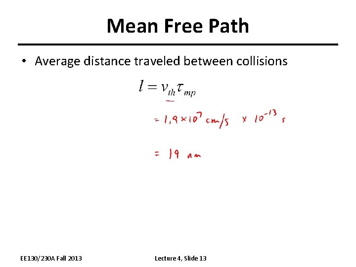
Mean Free Path • Average distance traveled between collisions EE 130/230 A Fall 2013 Lecture 4, Slide 13

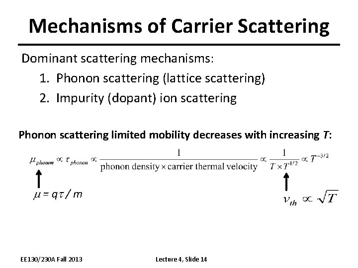
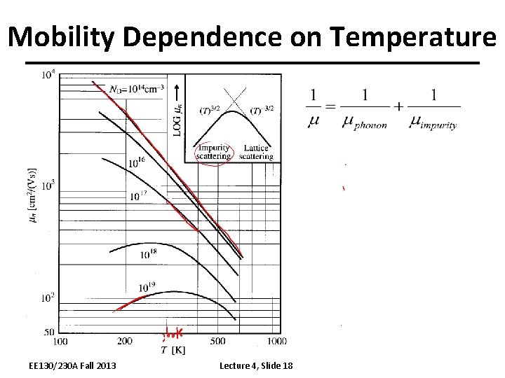
Mechanisms of Carrier Scattering Dominant scattering mechanisms: 1. Phonon scattering (lattice scattering) 2. Impurity (dopant) ion scattering Phonon scattering limited mobility decreases with increasing T: = q / m EE 130/230 A Fall 2013 Lecture 4, Slide 14

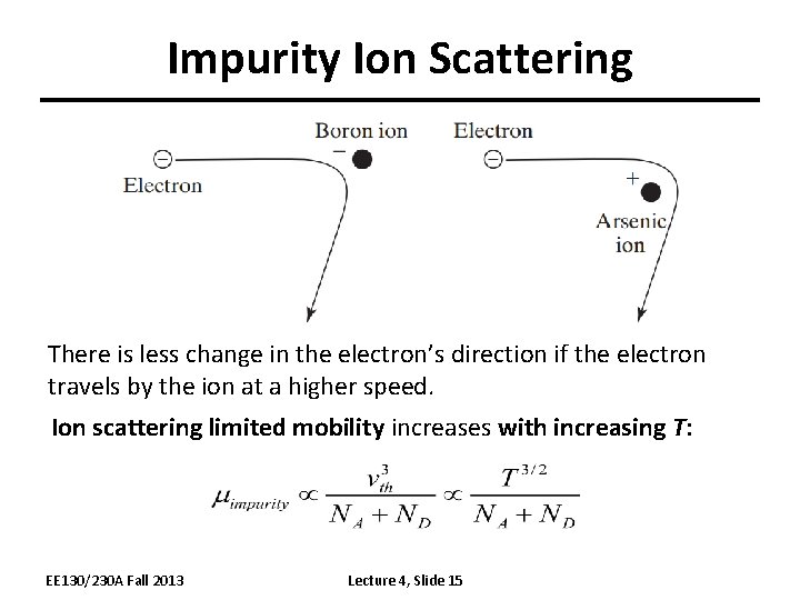
Impurity Ion Scattering There is less change in the electron’s direction if the electron travels by the ion at a higher speed. Ion scattering limited mobility increases with increasing T: EE 130/230 A Fall 2013 Lecture 4, Slide 15

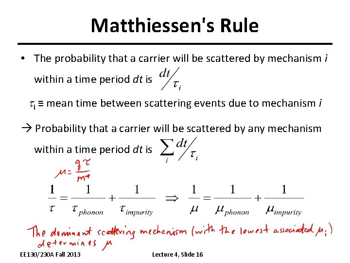
Matthiessen's Rule • The probability that a carrier will be scattered by mechanism i within a time period dt is i ≡ mean time between scattering events due to mechanism i Probability that a carrier will be scattered by any mechanism within a time period dt is EE 130/230 A Fall 2013 Lecture 4, Slide 16

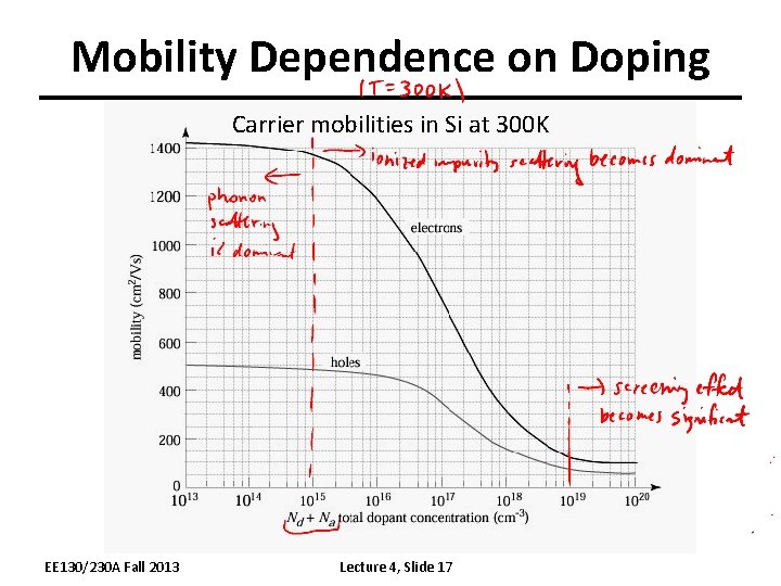
Mobility Dependence on Doping Carrier mobilities in Si at 300 K EE 130/230 A Fall 2013 Lecture 4, Slide 17

Mobility Dependence on Temperature EE 130/230 A Fall 2013 Lecture 4, Slide 18

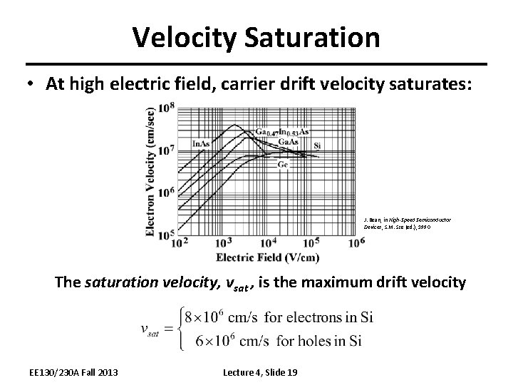
Velocity Saturation • At high electric field, carrier drift velocity saturates: J. Bean, in High-Speed Semiconductor Devices, S. M. Sze (ed. ), 1990 The saturation velocity, vsat , is the maximum drift velocity EE 130/230 A Fall 2013 Lecture 4, Slide 19

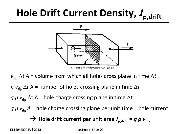
Hole Drift Current Density, Jp, drift R. F. Pierret, Semiconductor Fundamentals, Figure 3. 3 vdp Dt A = volume from which all holes cross plane in time Dt p vdp Dt A = number of holes crossing plane in time Dt q p vdp Dt A = hole charge crossing plane in time Dt q p vdp A = hole charge crossing plane per unit time = hole current Hole drift current per unit area Jp, drift = q p vdp EE 130/230 A Fall 2013 Lecture 4, Slide 20

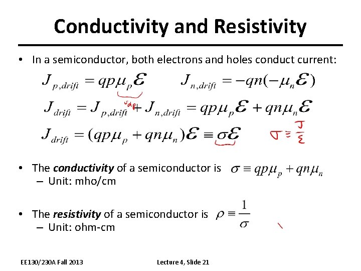
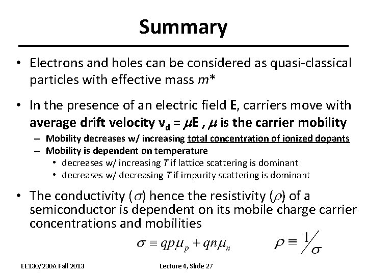
Conductivity and Resistivity • In a semiconductor, both electrons and holes conduct current: • The conductivity of a semiconductor is – Unit: mho/cm • The resistivity of a semiconductor is – Unit: ohm-cm EE 130/230 A Fall 2013 Lecture 4, Slide 21

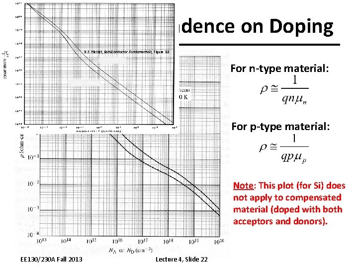
Resistivity Dependence on Doping R. F. Pierret, Semiconductor Fundamentals, Figure 3. 8 For n-type material: For p-type material: Note: This plot (for Si) does not apply to compensated material (doped with both acceptors and donors). EE 130/230 A Fall 2013 Lecture 4, Slide 22

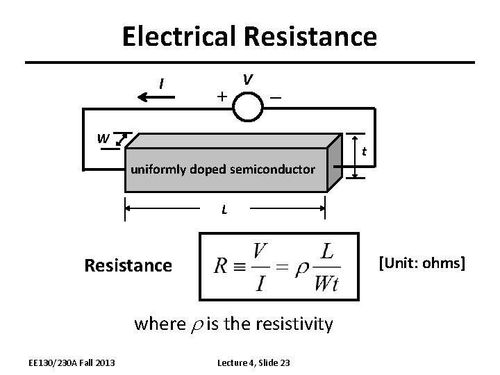
Electrical Resistance I + V _ W t uniformly doped semiconductor L Resistance [Unit: ohms] where is the resistivity EE 130/230 A Fall 2013 Lecture 4, Slide 23

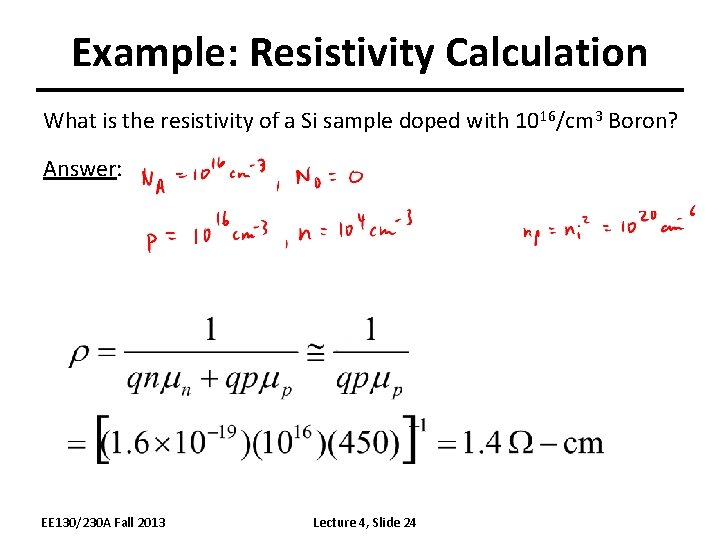
Example: Resistivity Calculation What is the resistivity of a Si sample doped with 1016/cm 3 Boron? Answer: EE 130/230 A Fall 2013 Lecture 4, Slide 24

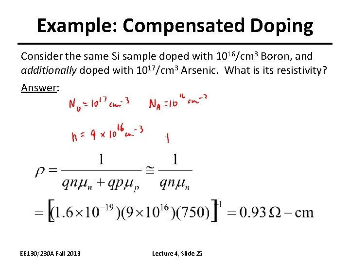
Example: Compensated Doping Consider the same Si sample doped with 1016/cm 3 Boron, and additionally doped with 1017/cm 3 Arsenic. What is its resistivity? Answer: EE 130/230 A Fall 2013 Lecture 4, Slide 25

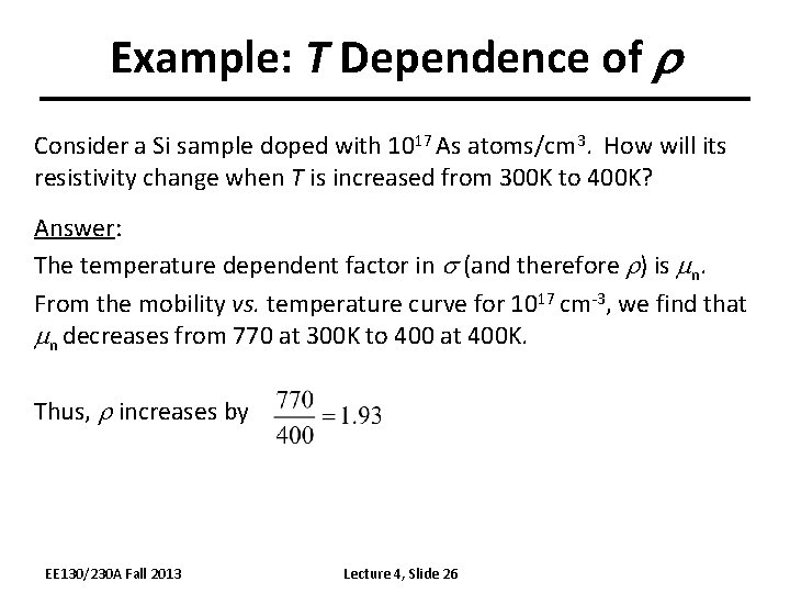
Example: T Dependence of r Consider a Si sample doped with 1017 As atoms/cm 3. How will its resistivity change when T is increased from 300 K to 400 K? Answer: The temperature dependent factor in (and therefore ) is n. From the mobility vs. temperature curve for 1017 cm-3, we find that n decreases from 770 at 300 K to 400 at 400 K. Thus, increases by EE 130/230 A Fall 2013 Lecture 4, Slide 26

Summary • Electrons and holes can be considered as quasi-classical particles with effective mass m* • In the presence of an electric field E, carriers move with average drift velocity vd = m. E , m is the carrier mobility – Mobility decreases w/ increasing total concentration of ionized dopants – Mobility is dependent on temperature • decreases w/ increasing T if lattice scattering is dominant • decreases w/ decreasing T if impurity scattering is dominant • The conductivity ( ) hence the resistivity ( ) of a semiconductor is dependent on its mobile charge carrier concentrations and mobilities EE 130/230 A Fall 2013 Lecture 4, Slide 27