LECTURE 4 HIGHEFFICIENCY POWER AMPLIFIER DESIGN 4 1
- Slides: 41

LECTURE 4. HIGH-EFFICIENCY POWER AMPLIFIER DESIGN 4. 1. Overdriven Class B 4. 2. Class F circuit design 4. 3. Inverse Class F 4. 4. Class E with shunt capacitance 4. 5. Class E with parallel circuit 4. 6. Class E with transmission lines 4. 7. Broadband Class E circuit design 4. 8. Practical high efficiency RF and microwave power amplifiers 1

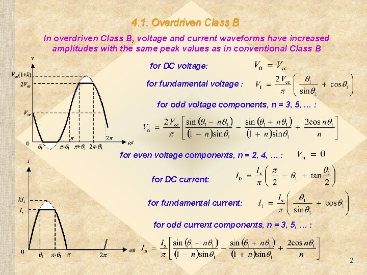
4. 1. Overdriven Class B In overdriven Class B, voltage and current waveforms have increased amplitudes with the same peak values as in conventional Class B for DC voltage: for fundamental voltage : for odd voltage components, n = 3, 5, … : for even voltage components, n = 2, 4, … : for DC current: for fundamental current: for odd current components, n = 3, 5, … : 2

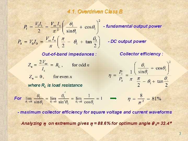
4. 1. Overdriven Class B - fundamental output power - DC output power Out-of-band impedances : Collector efficiency : where RL is load resistance For - maximum collector efficiency for square voltage and current waveforms Analyzing on extremum gives = 88. 6% for optimum angle 1= 32. 4 3

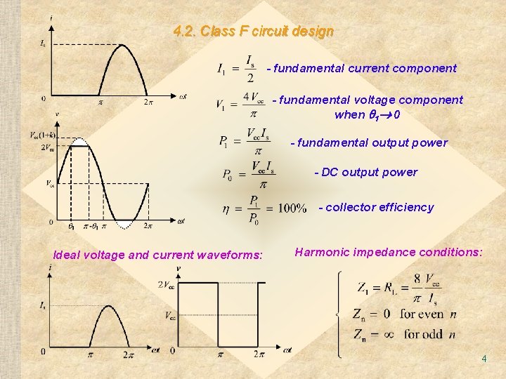
4. 2. Class F circuit design - fundamental current component - fundamental voltage component when 1 0 - fundamental output power - DC output power - collector efficiency Ideal voltage and current waveforms: Harmonic impedance conditions: 4

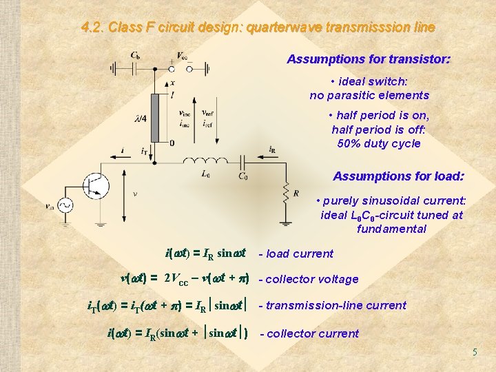
4. 2. Class F circuit design: quarterwave transmisssion line Assumptions for transistor: • ideal switch: no parasitic elements • half period is on, half period is off: 50% duty cycle Assumptions for load: • purely sinusoidal current: ideal L 0 C 0 -circuit tuned at fundamental i( t) = IR sin t - load current v( t) = 2 Vcc – v( t + ) - collector voltage i. T( t) = i. T( t + ) = IR sin t - transmission-line current i( t) = IR(sin t + sin t ) - collector current 5

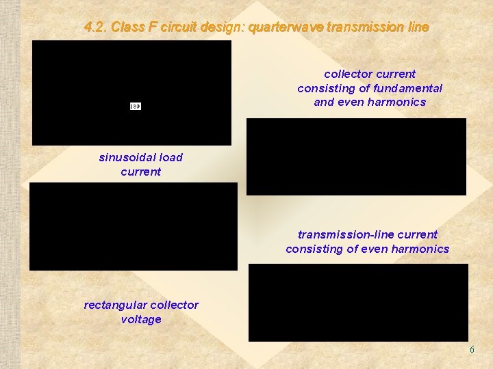
4. 2. Class F circuit design: quarterwave transmission line collector current consisting of fundamental and even harmonics sinusoidal load current transmission-line current consisting of even harmonics rectangular collector voltage 6

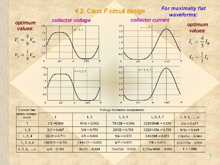
4. 2. Class F circuit design optimum values: collector voltage For maximally flat waveforms: collector current optimum values: 7

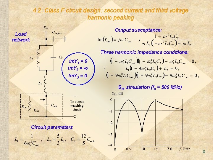
4. 2. Class F circuit design: second current and third voltage harmonic peaking Output susceptance: Load network Three harmonic impedance conditions: Im. Y 1 = 0 Im. Y 2 = Im. Y 3 = 0 S 21 simulation (f 0 = 500 MHz) Circuit parameters 8

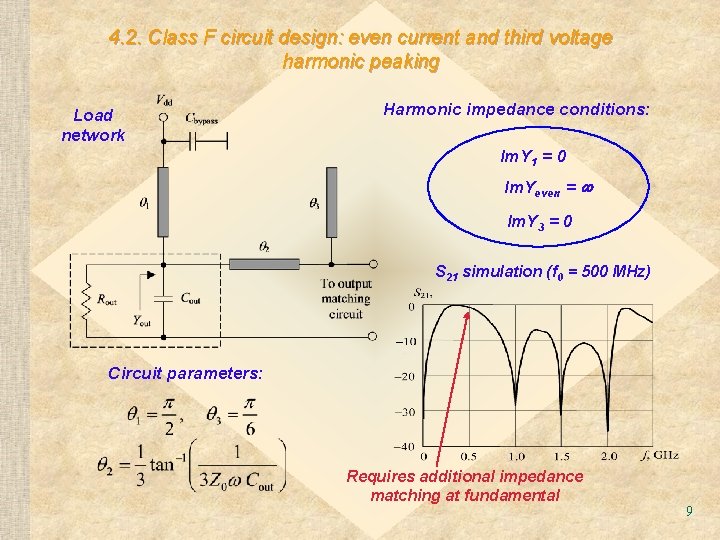
4. 2. Class F circuit design: even current and third voltage harmonic peaking Load network Harmonic impedance conditions: Im. Y 1 = 0 Im. Yeven = Im. Y 3 = 0 S 21 simulation (f 0 = 500 MHz) Circuit parameters: Requires additional impedance matching at fundamental 9

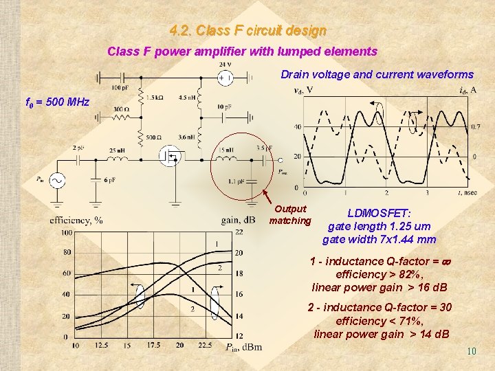
4. 2. Class F circuit design Class F power amplifier with lumped elements Drain voltage and current waveforms f 0 = 500 MHz Output matching LDMOSFET: gate length 1. 25 um gate width 7 x 1. 44 mm 1 - inductance Q-factor = efficiency > 82%, linear power gain > 16 d. B 2 - inductance Q-factor = 30 efficiency < 71%, linear power gain > 14 d. B 10

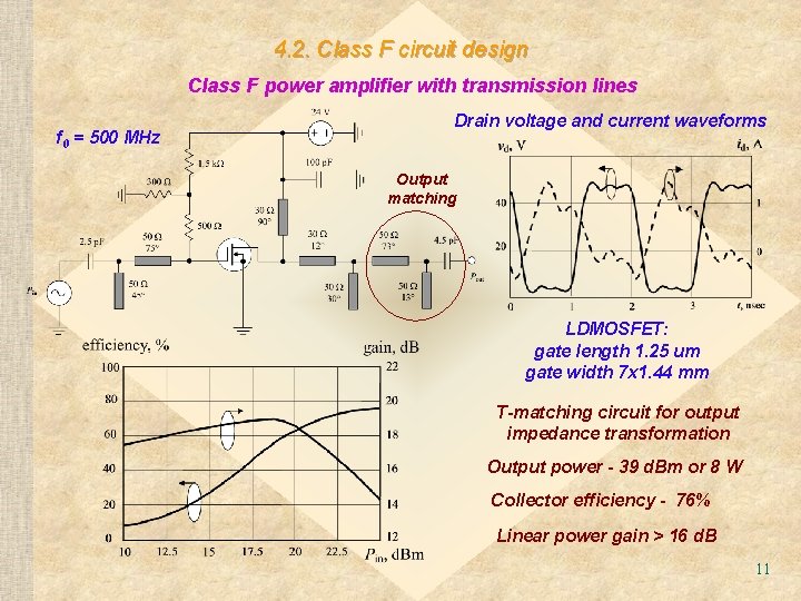
4. 2. Class F circuit design Class F power amplifier with transmission lines f 0 = 500 MHz Drain voltage and current waveforms Output matching LDMOSFET: gate length 1. 25 um gate width 7 x 1. 44 mm T-matching circuit for output impedance transformation Output power - 39 d. Bm or 8 W Collector efficiency - 76% Linear power gain > 16 d. B 11

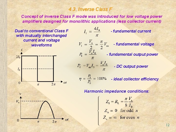
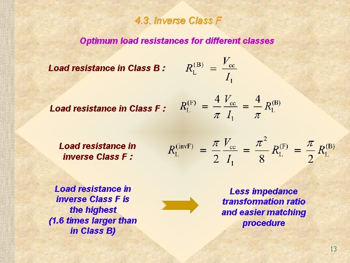
4. 3. Inverse Class F Concept of inverse Class F mode was introduced for low voltage power amplifiers designed for monolithic applications (less collector current) Dual to conventional Class F with mutually interchanged current and voltage waveforms - fundamental current - fundamental voltage - fundamental output power - DC output power - ideal collector efficiency Harmonic impedance conditions: 12

4. 3. Inverse Class F Optimum load resistances for different classes Load resistance in Class B : Load resistance in Class F : Load resistance in inverse Class F is the highest (1. 6 times larger than in Class B) Less impedance transformation ratio and easier matching procedure 13

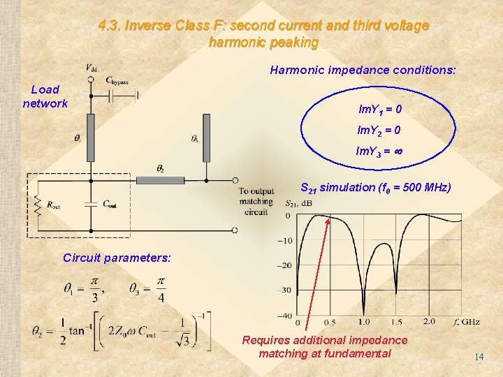
4. 3. Inverse Class F: second current and third voltage harmonic peaking Harmonic impedance conditions: Load network Im. Y 1 = 0 Im. Y 2 = 0 Im. Y 3 = S 21 simulation (f 0 = 500 MHz) Circuit parameters: Requires additional impedance matching at fundamental 14

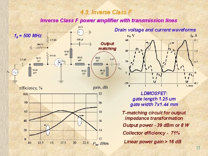
4. 3. Inverse Class F power amplifier with transmission lines Drain voltage and current waveforms f 0 = 500 MHz Output matching LDMOSFET: gate length 1. 25 um gate width 7 x 1. 44 mm T-matching circuit for output impedance transformation Output power - 39 d. Bm or 8 W Collector efficiency - 71% Linear power gain > 16 d. B 15

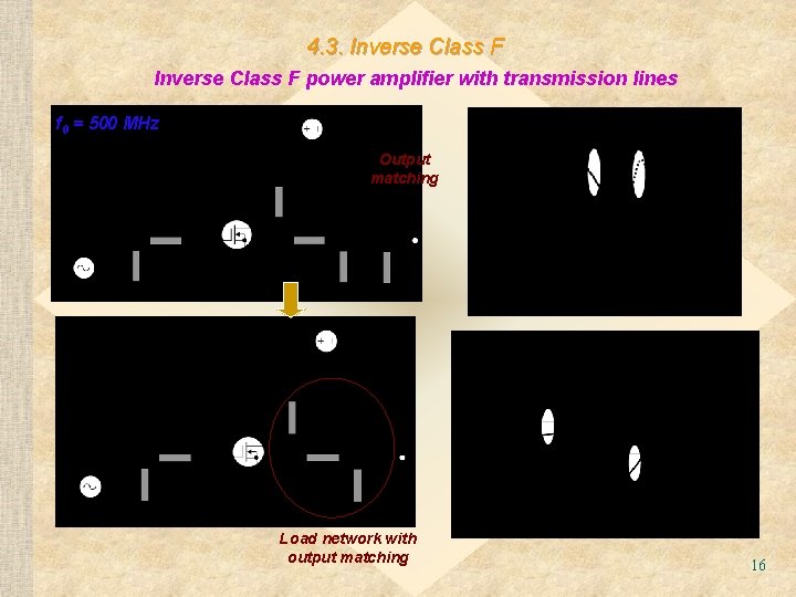
4. 3. Inverse Class F power amplifier with transmission lines f 0 = 500 MHz Output matching Load network with output matching 16

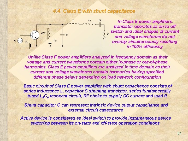
4. 4. Class E with shunt capacitance In Class E power amplifiers, transistor operates as on-to-off switch and ideal shapes of current and voltage waveforms do not overlap simultaneously resulting in 100% efficiency Unlike Class F power amplifiers analyzed in frequency domain as their voltage and current waveforms contain either in-phase or out-of-phase harmonics, Class E power amplifiers are analyzed in time domain as their current and voltage waveforms contain harmonics having specified different phase delays depending on load network configuration Basic circuit of Class E power amplifier with shunt capacitance consists of series inductance L, capacitor C shunting transistor, series fundamentally tuned L 0 C 0 resonant circuit, RF choke to supply DC current and load R Shunt capacitor C can represent intrinsic device output capacitance and external circuit capacitance Active device is considered as ideal switch to provide instantaneous device switching between its on-state and off-state operation conditions 17

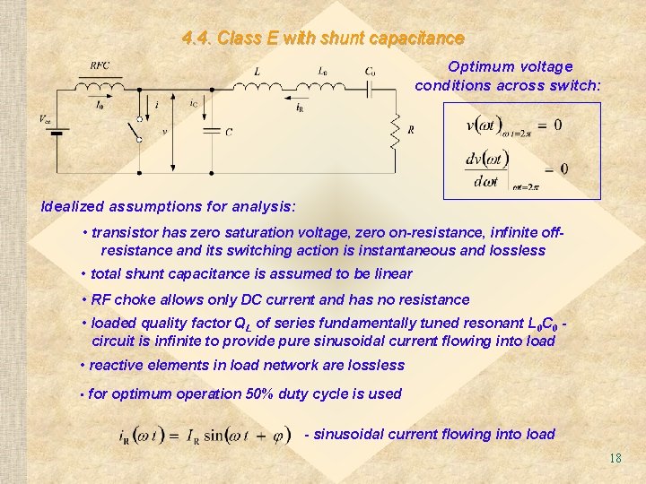
4. 4. Class E with shunt capacitance Optimum voltage conditions across switch: Idealized assumptions for analysis: • transistor has zero saturation voltage, zero on-resistance, infinite offresistance and its switching action is instantaneous and lossless • total shunt capacitance is assumed to be linear • RF choke allows only DC current and has no resistance • loaded quality factor QL of series fundamentally tuned resonant L 0 C 0 circuit is infinite to provide pure sinusoidal current flowing into load • reactive elements in load network are lossless • for optimum operation 50% duty cycle is used - sinusoidal current flowing into load 18

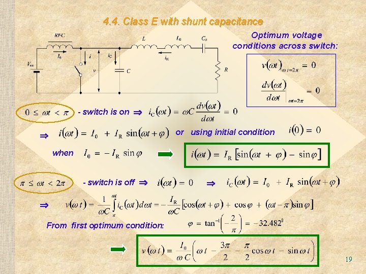
4. 4. Class E with shunt capacitance Optimum voltage conditions across switch: - switch is on or using initial condition when - switch is off From first optimum condition: 19

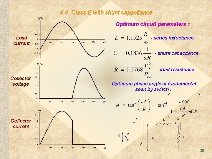
4. 4. Class E with shunt capacitance Optimum circuit parameters : Load current - series inductance - shunt capacitance - load resistance Collector voltage Optimum phase angle at fundamental seen by switch : Collector current 20

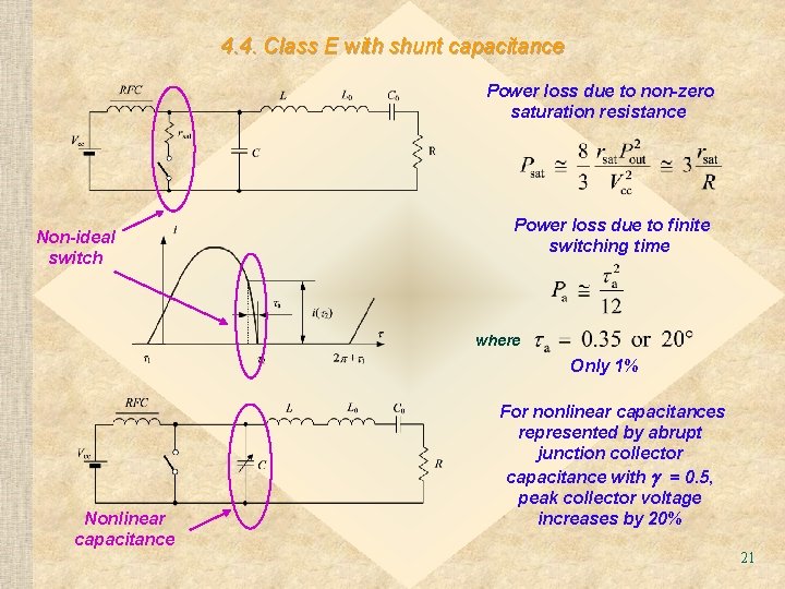
4. 4. Class E with shunt capacitance Power loss due to non-zero saturation resistance Non-ideal switch Power loss due to finite switching time where Only 1% Nonlinear capacitance For nonlinear capacitances represented by abrupt junction collector capacitance with = 0. 5, peak collector voltage increases by 20% 21

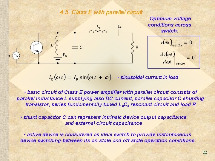
4. 5. Class E with parallel circuit Optimum voltage conditions across switch: - sinusoidal current in load • basic circuit of Class E power amplifier with parallel circuit consists of parallel inductance L supplying also DC current, parallel capacitor C shunting transistor, series fundamentally tuned L 0 C 0 resonant circuit and load R • shunt capacitor C can represent intrinsic device output capacitance and external circuit capacitance • active device is considered as ideal switch to provide instantaneous device switching between its on-state and off-state operation conditions 22

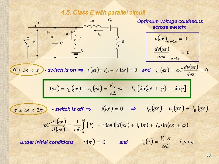
4. 5. Class E with parallel circuit Optimum voltage conditions across switch: - switch is on and - switch is off under initial conditions and 23

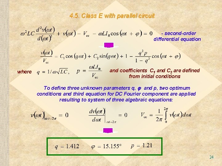
4. 5. Class E with parallel circuit - second-order differential equation where and coefficients C 1 and C 2 are defined from initial conditions To define three unknown parameters q, and p, two optimum conditions and third equation for DC Fourier component are applied resulting to system of three algebraic equations: 24

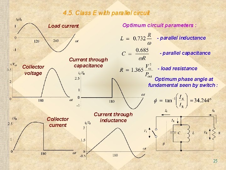
4. 5. Class E with parallel circuit Optimum circuit parameters : Load current - parallel inductance - parallel capacitance Current through capacitance Collector voltage - load resistance Optimum phase angle at fundamental seen by switch : Collector current Current through inductance 25

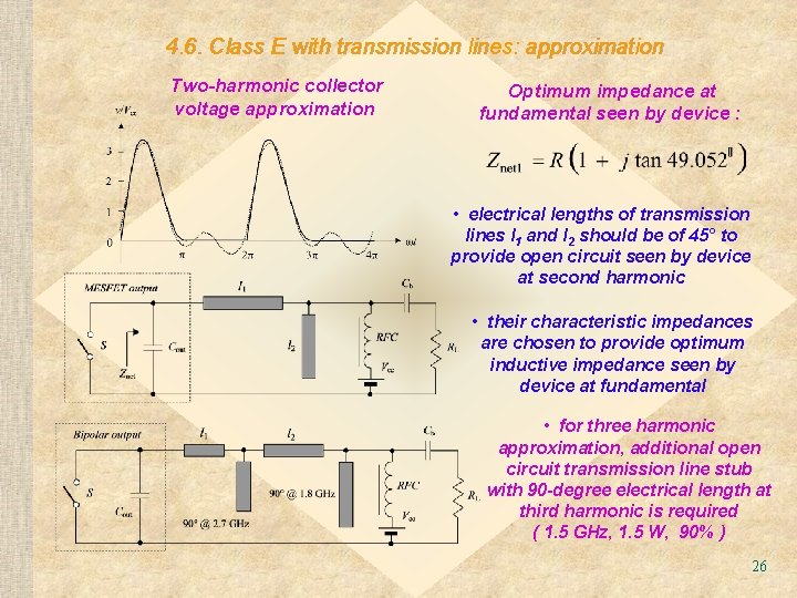
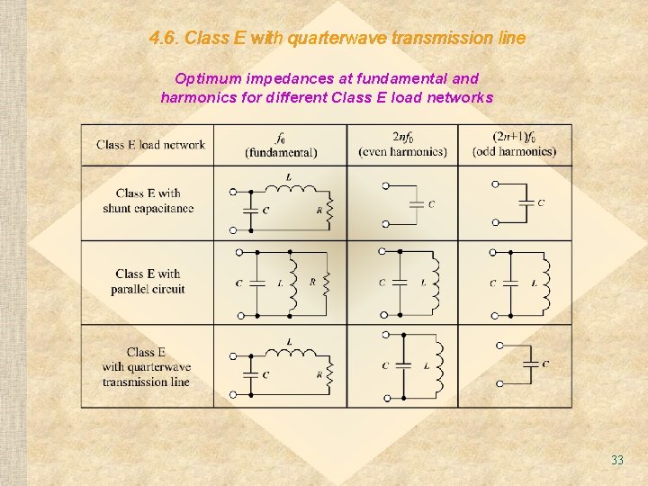
4. 6. Class E with transmission lines: approximation Two-harmonic collector voltage approximation Optimum impedance at fundamental seen by device : • electrical lengths of transmission lines l 1 and l 2 should be of 45° to provide open circuit seen by device at second harmonic • their characteristic impedances are chosen to provide optimum inductive impedance seen by device at fundamental • for three harmonic approximation, additional open circuit transmission line stub with 90 -degree electrical length at third harmonic is required ( 1. 5 GHz, 1. 5 W, 90% ) 26

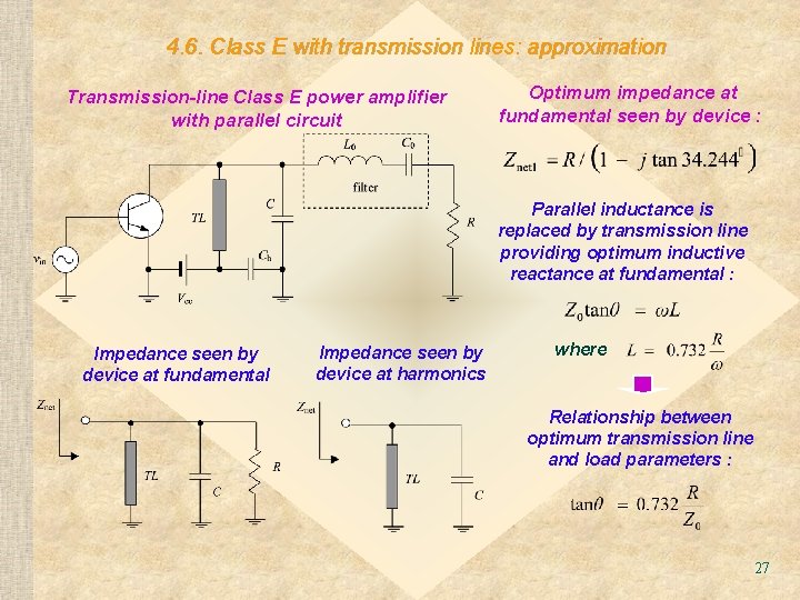
4. 6. Class E with transmission lines: approximation Transmission-line Class E power amplifier with parallel circuit Optimum impedance at fundamental seen by device : Parallel inductance is replaced by transmission line providing optimum inductive reactance at fundamental : Impedance seen by device at fundamental Impedance seen by device at harmonics where Relationship between optimum transmission line and load parameters : 27

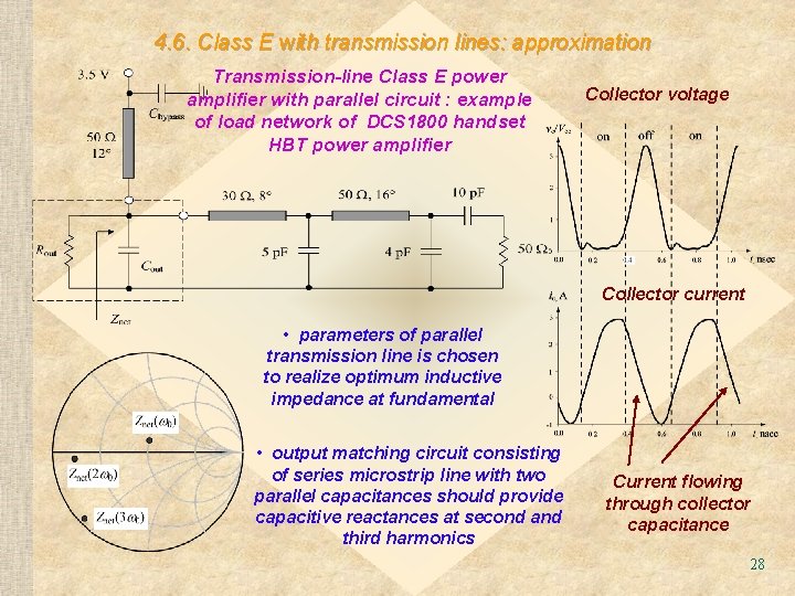
4. 6. Class E with transmission lines: approximation Transmission-line Class E power amplifier with parallel circuit : example of load network of DCS 1800 handset HBT power amplifier Collector voltage Collector current • parameters of parallel transmission line is chosen to realize optimum inductive impedance at fundamental • output matching circuit consisting of series microstrip line with two parallel capacitances should provide capacitive reactances at second and third harmonics Current flowing through collector capacitance 28

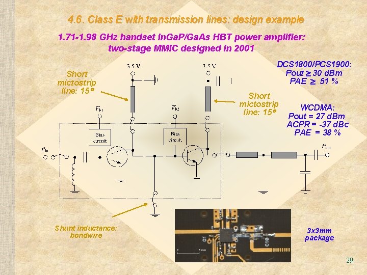
4. 6. Class E with transmission lines: design example 1. 71 -1. 98 GHz handset In. Ga. P/Ga. As HBT power amplifier: two-stage MMIC designed in 2001 Short mictostrip line: 15 Shunt inductance: bondwire DCS 1800/PCS 1900: Pout 30 d. Bm PAE 51 % Short mictostrip line: 15 WCDMA: Pout = 27 d. Bm ACPR = -37 d. Bc PAE = 38 % 3 x 3 mm package 29

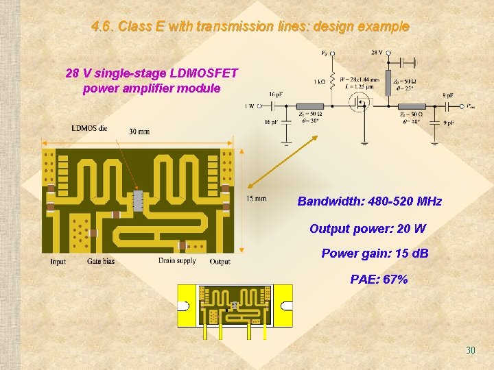
4. 6. Class E with transmission lines: design example 28 V single-stage LDMOSFET power amplifier module Bandwidth: 480 -520 MHz Output power: 20 W Power gain: 15 d. B PAE: 67% 30

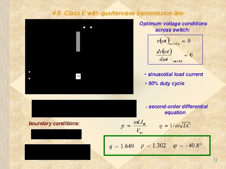
4. 6. Class E with quarterwave transmission line Optimum voltage conditions across switch: • sinusoidal load current • 50% duty cycle - second-order differential equation boundary conditions: 31

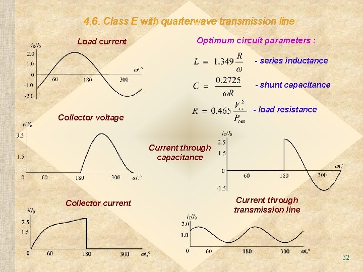
4. 6. Class E with quarterwave transmission line Load current Optimum circuit parameters : - series inductance - shunt capacitance - load resistance Collector voltage Current through capacitance Collector current Current through transmission line 32

4. 6. Class E with quarterwave transmission line Optimum impedances at fundamental and harmonics for different Class E load networks 33

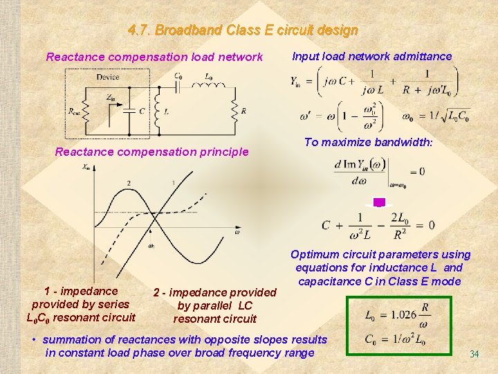
4. 7. Broadband Class E circuit design Reactance compensation load network Reactance compensation principle 1 - impedance provided by series L 0 C 0 resonant circuit 2 - impedance provided by parallel LC resonant circuit Input load network admittance To maximize bandwidth: Optimum circuit parameters using equations for inductance L and capacitance C in Class E mode • summation of reactances with opposite slopes results in constant load phase over broad frequency range 34

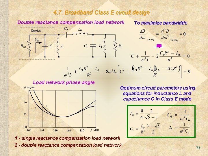
4. 7. Broadband Class E circuit design Double reactance compensation load network To maximize bandwidth: Load network phase angle Optimum circuit parameters using equations for inductance L and capacitance C in Class E mode 1 - single reactance compensation load network 2 - double reactance compensation load network 35

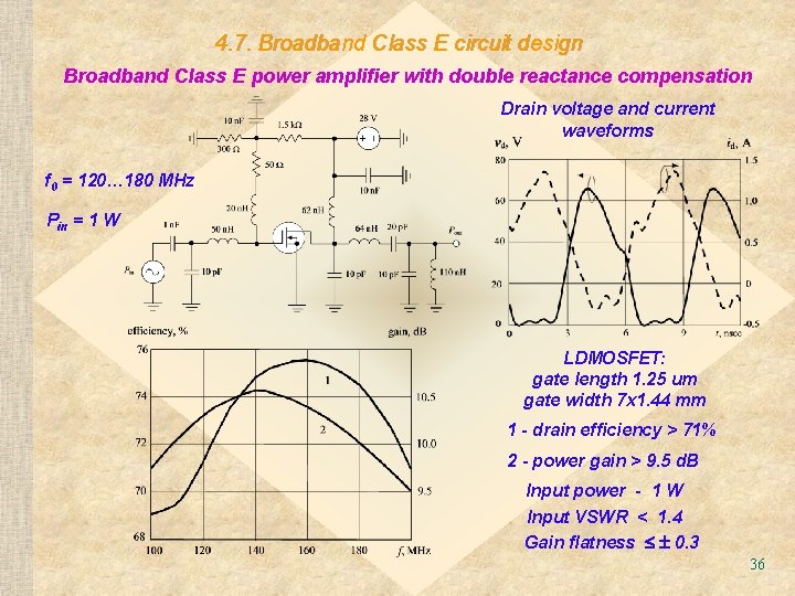
4. 7. Broadband Class E circuit design Broadband Class E power amplifier with double reactance compensation Drain voltage and current waveforms f 0 = 120… 180 MHz Pin = 1 W LDMOSFET: gate length 1. 25 um gate width 7 x 1. 44 mm 1 - drain efficiency > 71% 2 - power gain > 9. 5 d. B Input power - 1 W Input VSWR < 1. 4 Gain flatness 0. 3 36

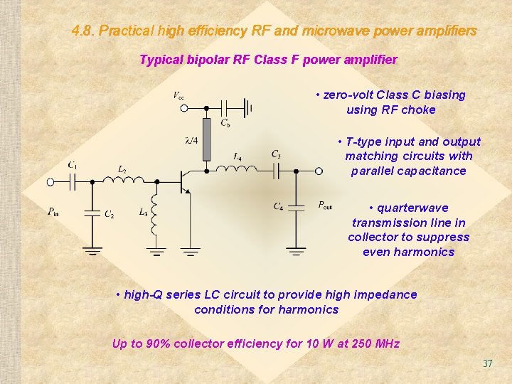
4. 8. Practical high efficiency RF and microwave power amplifiers Typical bipolar RF Class F power amplifier • zero-volt Class C biasing using RF choke • T-type input and output matching circuits with parallel capacitance • quarterwave transmission line in collector to suppress even harmonics • high-Q series LC circuit to provide high impedance conditions for harmonics Up to 90% collector efficiency for 10 W at 250 MHz 37

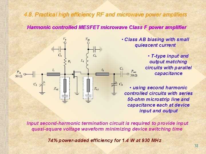
4. 8. Practical high efficiency RF and microwave power amplifiers Harmonic controlled MESFET microwave Class F power amplifier • Class AB biasing with small quiescent current • T-type input and output matching circuits with parallel capacitance • using second harmonic controlled circuits with series 50 -ohm microstrip line and capacitance each at device input and output Input second-harmonic termination circuit is required to provide input quasi-square voltage waveform minimizing device switching time 74% power-added efficiency for 1. 4 W at 930 MHz 38

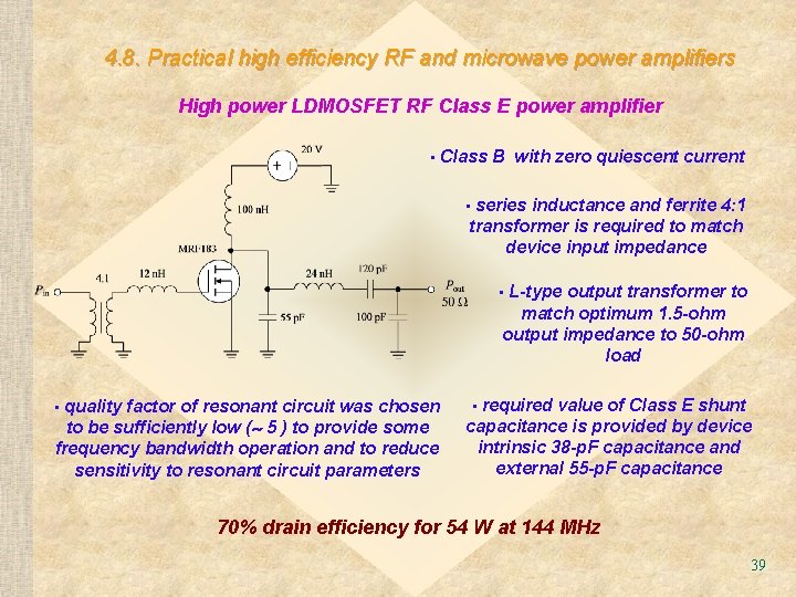
4. 8. Practical high efficiency RF and microwave power amplifiers High power LDMOSFET RF Class E power amplifier • Class B with zero quiescent current • series inductance and ferrite 4: 1 transformer is required to match device input impedance • L-type output transformer to match optimum 1. 5 -ohm output impedance to 50 -ohm load • quality factor of resonant circuit was chosen to be sufficiently low ( 5 ) to provide some frequency bandwidth operation and to reduce sensitivity to resonant circuit parameters • required value of Class E shunt capacitance is provided by device intrinsic 38 -p. F capacitance and external 55 -p. F capacitance 70% drain efficiency for 54 W at 144 MHz 39

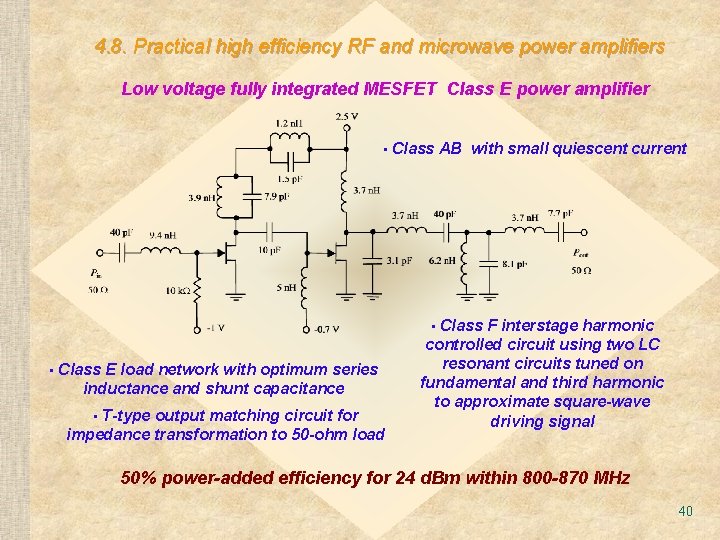
4. 8. Practical high efficiency RF and microwave power amplifiers Low voltage fully integrated MESFET Class E power amplifier • Class AB with small quiescent current • Class F interstage harmonic • Class E load network with optimum series inductance and shunt capacitance • T-type output matching circuit for impedance transformation to 50 -ohm load controlled circuit using two LC resonant circuits tuned on fundamental and third harmonic to approximate square-wave driving signal 50% power-added efficiency for 24 d. Bm within 800 -870 MHz 40

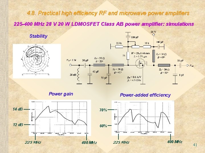
4. 8. Practical high efficiency RF and microwave power amplifiers 225 -400 MHz 28 V 20 W LDMOSFET Class AB power amplifier: simulations Stability Power gain Power-added efficiency 14 d. B 70% 12 d. B 60% 225 MHz 400 MHz 41