Lecture 34 OUTLINE The MOS Capacitor MOS nonidealities
- Slides: 10

Lecture #34 OUTLINE The MOS Capacitor: • MOS non-idealities (cont. ) • VT adjustment Reading: Chapter 18. 3 1 Spring 2007 EE 130 Lecture 34, Slide 1

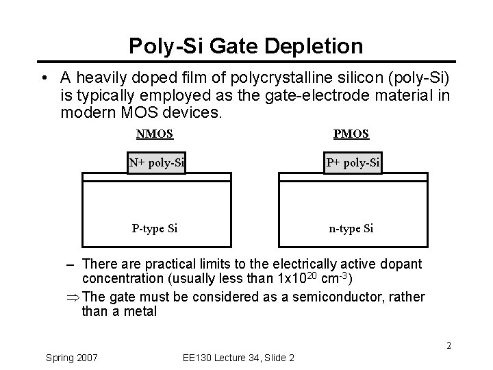
Poly-Si Gate Depletion • A heavily doped film of polycrystalline silicon (poly-Si) is typically employed as the gate-electrode material in modern MOS devices. NMOS PMOS N+ poly-Si P-type Si n-type Si – There are practical limits to the electrically active dopant concentration (usually less than 1 x 1020 cm-3) Þ The gate must be considered as a semiconductor, rather than a metal 2 Spring 2007 EE 130 Lecture 34, Slide 2

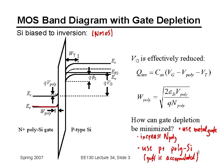
MOS Band Diagram with Gate Depletion Si biased to inversion: WT Ec q. Vpoly qf. S VG is effectively reduced: EFS Ev q. VG Ec Ev Wpoly N+ poly-Si gate P-type Si How can gate depletion be minimized? 3 Spring 2007 EE 130 Lecture 34, Slide 3

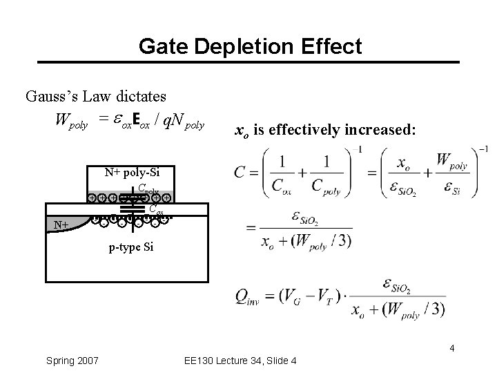
Gate Depletion Effect Gauss’s Law dictates Wpoly = e ox. Eox / q. N poly xo is effectively increased: N+ poly-Si Cpoly + + + + Cox N+ - - - - - p-type Si 4 Spring 2007 EE 130 Lecture 34, Slide 4

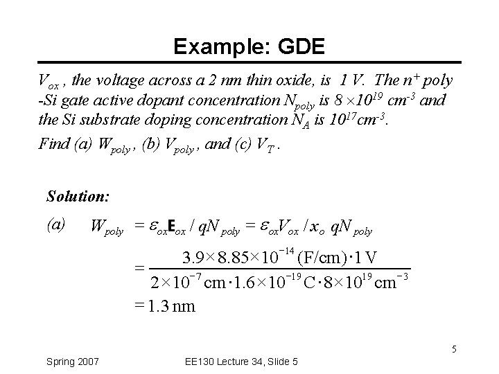
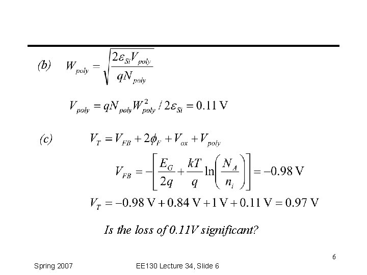
Example: GDE Vox , the voltage across a 2 nm thin oxide, is 1 V. The n+ poly -Si gate active dopant concentration Npoly is 8 1019 cm-3 and the Si substrate doping concentration NA is 1017 cm-3. Find (a) Wpoly , (b) Vpoly , and (c) VT. Solution: (a) Wpoly = e ox. Eox / q. N poly = e ox. Vox / x o q. N poly - 3. 9 8. 85 10 14 (F/cm) × 1 V = -7 -19 -3 19 × × 2 10 cm 1. 6 10 C 8 10 cm = 1. 3 nm 5 Spring 2007 EE 130 Lecture 34, Slide 5

(b) (c) Is the loss of 0. 11 V significant? 6 Spring 2007 EE 130 Lecture 34, Slide 6

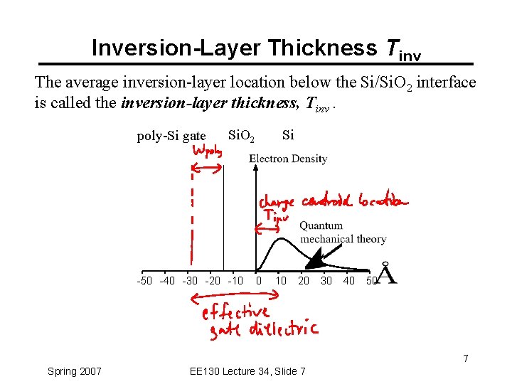
Inversion-Layer Thickness Tinv The average inversion-layer location below the Si/Si. O 2 interface is called the inversion-layer thickness, Tinv. poly-Si gate Si. O 2 -50 -40 -30 -20 -10 Si 0 10 20 30 40 50 7 Spring 2007 EE 130 Lecture 34, Slide 7

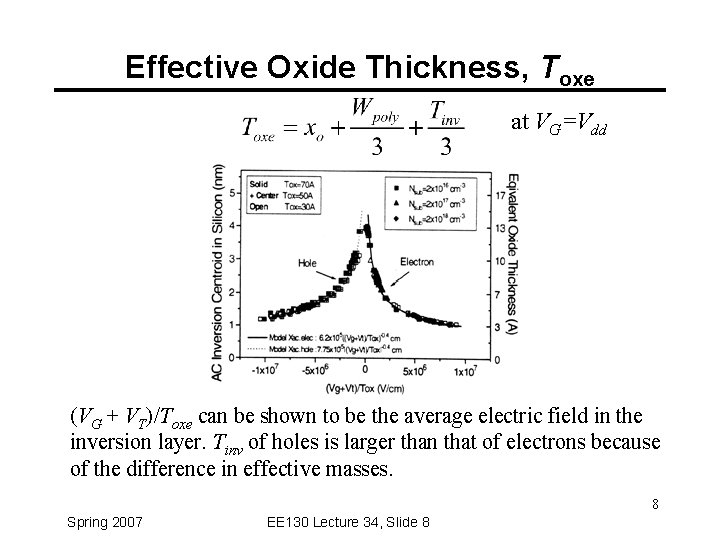
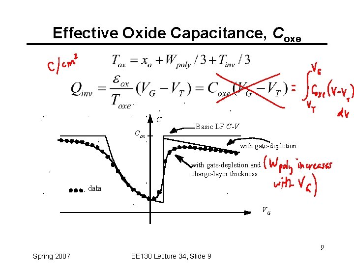
Effective Oxide Thickness, Toxe at VG=Vdd (VG + VT)/Toxe can be shown to be the average electric field in the inversion layer. Tinv of holes is larger than that of electrons because of the difference in effective masses. 8 Spring 2007 EE 130 Lecture 34, Slide 8

Effective Oxide Capacitance, Coxe C Cox Basic LF C-V with gate-depletion and charge-layer thickness data VG 9 Spring 2007 EE 130 Lecture 34, Slide 9

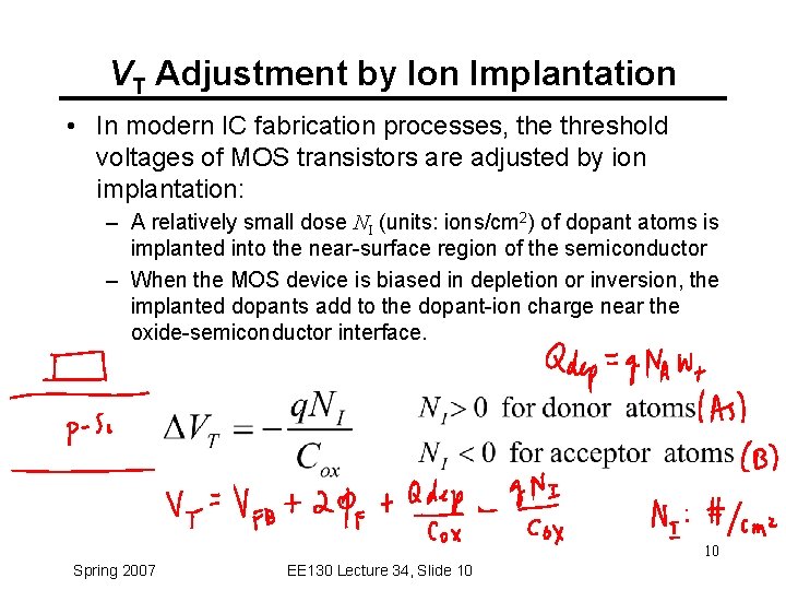
VT Adjustment by Ion Implantation • In modern IC fabrication processes, the threshold voltages of MOS transistors are adjusted by ion implantation: – A relatively small dose NI (units: ions/cm 2) of dopant atoms is implanted into the near-surface region of the semiconductor – When the MOS device is biased in depletion or inversion, the implanted dopants add to the dopant-ion charge near the oxide-semiconductor interface. 10 Spring 2007 EE 130 Lecture 34, Slide 10