Lecture 30 IEEE 1149 4 JTAG Analog Test
- Slides: 34

Lecture 30 IEEE 1149. 4 JTAG Analog Test Access Port and Standard n n n n Motivation Bus overview Hardware faults Test Bus Interface Circuit (TBIC) Analog Boundary Module (ABM) Instructions Specialized Bus Circuits Summary Copyright 2001, Agrawal & Bushnell VLSI Test: Lecture 30 1

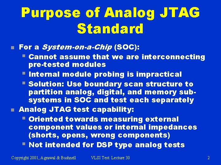
Purpose of Analog JTAG Standard n n For a System-on-a-Chip (SOC): § Cannot assume that we are interconnecting pre-tested modules § Internal module probing is impractical § Solution: Use boundary scan structure to partition analog, digital, and memory subsystems in SOC and test each separately Analog JTAG test capability: § Oriented towards measuring external component values or internal impedances (shorts, opens, wrong components) § Not intended for DSP type analog tests Copyright 2001, Agrawal & Bushnell VLSI Test: Lecture 30 2

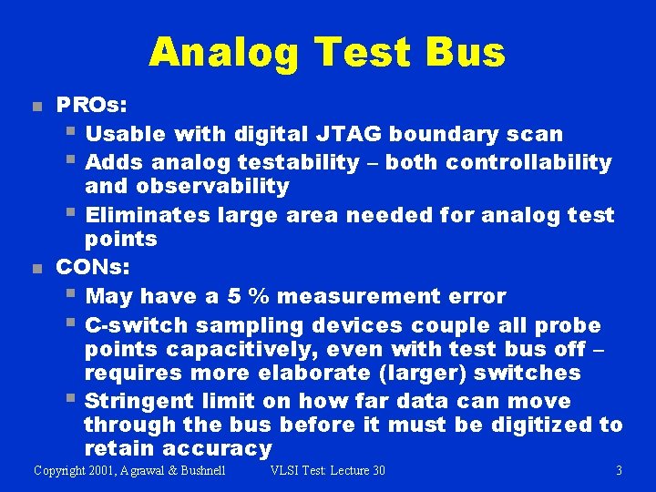
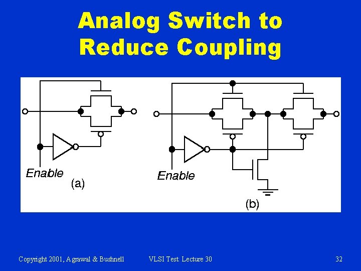
Analog Test Bus n n PROs: § Usable with digital JTAG boundary scan § Adds analog testability – both controllability and observability § Eliminates large area needed for analog test points CONs: § May have a 5 % measurement error § C-switch sampling devices couple all probe points capacitively, even with test bus off – requires more elaborate (larger) switches § Stringent limit on how far data can move through the bus before it must be digitized to retain accuracy Copyright 2001, Agrawal & Bushnell VLSI Test: Lecture 30 3

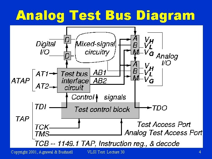
Analog Test Bus Diagram Copyright 2001, Agrawal & Bushnell VLSI Test: Lecture 30 4

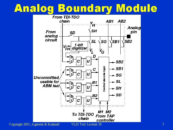
Analog Boundary Module Copyright 2001, Agrawal & Bushnell VLSI Test: Lecture 30 5

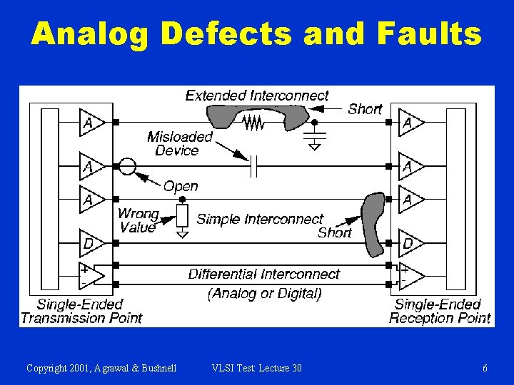
Analog Defects and Faults Copyright 2001, Agrawal & Bushnell VLSI Test: Lecture 30 6

Need for Discrete Components n n n Impedance matching of transmission lines necessary – merchant ICs will not have built-in impedance matching resistances Discrete resistors use much power – may prevent them from being on-chip Impossible to make high-valued, accurate inductors or transformers on chip Integrated R, C, L components are never as precise as external ones Some ICs can be extended to more functions if external R, C, or L value can be changed Copyright 2001, Agrawal & Bushnell VLSI Test: Lecture 30 7

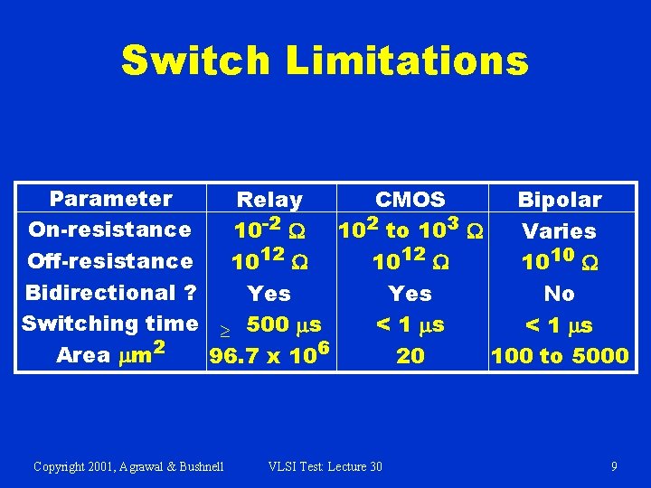
Measurement Limitations with 1149. 4 n n n Must test device with power on Multiplexing done with silicon devices, not relays Introduces unwanted impedances during testing Has additional current leakages to ground CMOS silicon switches non-linear over larger signal swings – may also be slow 1149. 4 bus has less than 1 MHz bandwidth Copyright 2001, Agrawal & Bushnell VLSI Test: Lecture 30 8

Switch Limitations Parameter Relay CMOS Bipolar On-resistance 10 -2 W 102 to 103 W Varies Off-resistance 1012 W 1010 W Bidirectional ? Yes No Switching time ³ 500 ms < 1 ms Area mm 2 96. 7 x 10⁶ 20 100 to 5000 Copyright 2001, Agrawal & Bushnell VLSI Test: Lecture 30 9

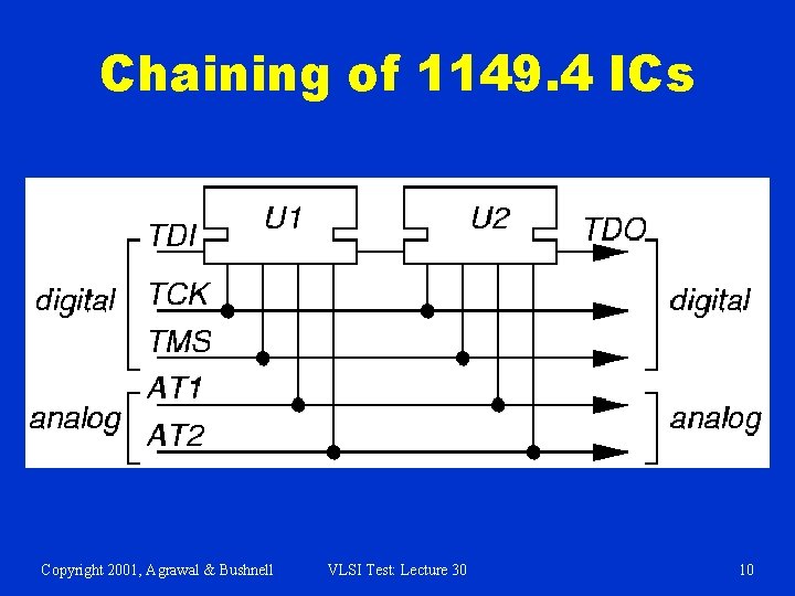
Chaining of 1149. 4 ICs Copyright 2001, Agrawal & Bushnell VLSI Test: Lecture 30 10

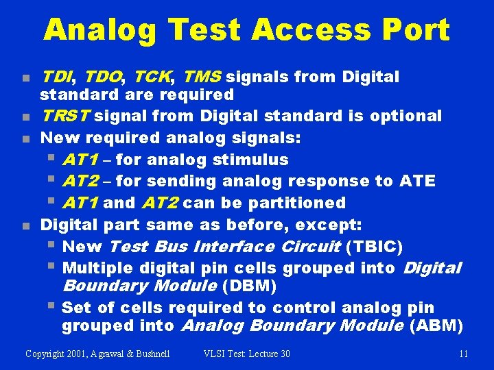
Analog Test Access Port n n TDI, TDO, TCK, TMS signals from Digital standard are required TRST signal from Digital standard is optional New required analog signals: § AT 1 – for analog stimulus § AT 2 – for sending analog response to ATE § AT 1 and AT 2 can be partitioned Digital part same as before, except: § New Test Bus Interface Circuit (TBIC) § Multiple digital pin cells grouped into Digital Boundary Module (DBM) § Set of cells required to control analog pin grouped into Analog Boundary Module (ABM) Copyright 2001, Agrawal & Bushnell VLSI Test: Lecture 30 11

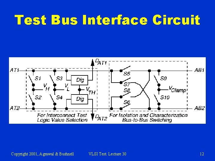
Test Bus Interface Circuit Copyright 2001, Agrawal & Bushnell VLSI Test: Lecture 30 12

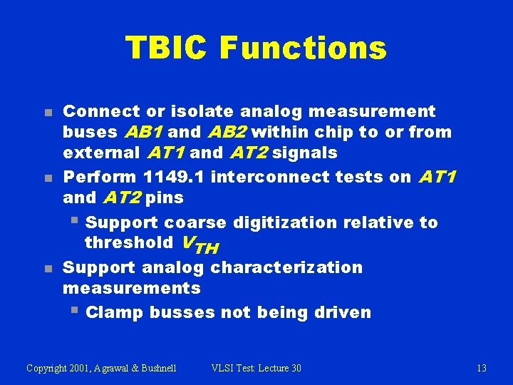
TBIC Functions n n n Connect or isolate analog measurement buses AB 1 and AB 2 within chip to or from external AT 1 and AT 2 signals Perform 1149. 1 interconnect tests on AT 1 and AT 2 pins § Support coarse digitization relative to threshold VTH Support analog characterization measurements § Clamp busses not being driven Copyright 2001, Agrawal & Bushnell VLSI Test: Lecture 30 13

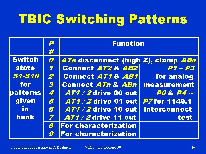
TBIC Switching Patterns P # Switch 0 state 1 S 1 -S 10 2 for 3 patterns 4 given 5 in 6 book 7 8 9 Function ATn disconnect (high Z), clamp ABn Connect AT 2 & AB 2 P 1 – P 3 Connect AT 1 & AB 1 for analog Connect ATn & ABn measurement AT 1 / 2 drive 00 out P 0 & P 4 -AT 1 / 2 drive 01 out P 7 for 1149. 1 AT 1 / 2 drive 10 out interconnect AT 1 / 2 drive 11 out test For characterization Copyright 2001, Agrawal & Bushnell VLSI Test: Lecture 30 14

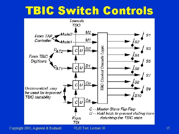
TBIC Switch Controls Copyright 2001, Agrawal & Bushnell VLSI Test: Lecture 30 15

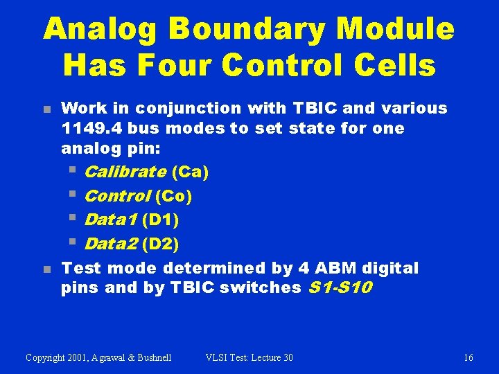
Analog Boundary Module Has Four Control Cells n n Work in conjunction with TBIC and various 1149. 4 bus modes to set state for one analog pin: § Calibrate (Ca) § Control (Co) § Data 1 (D 1) § Data 2 (D 2) Test mode determined by 4 ABM digital pins and by TBIC switches S 1 -S 10 Copyright 2001, Agrawal & Bushnell VLSI Test: Lecture 30 16

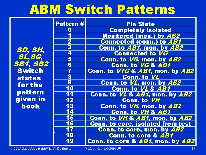
ABM Switch Patterns SD, SH, SL, SG, SB 1, SB 2 Switch states for the pattern given in book Pattern # Pin State 0 Completely isolated 1 Monitored (mon. ) by AB 2 2 Connected (conn. ) to AB 1 3 Conn. to AB 1, mon. by AB 2 4 Connected to VG 5 Conn. to VG, mon. by AB 2 6 Conn. to VG & AB 1 7 Conn. to VTG & AB 1, mon. by AB 2 8 Conn. to VL 9 Conn. to VL, mon. by AB 2 10 Conn. to VL & AB 1 11 Conn. to VL & AB 1, mon. by AB 2 12 Conn. to VH 13 Conn. to VH, mon. by AB 2 14 Conn. to VH & AB 1 15 Conn. to VH & AB 1, mon. by AB 2 16 Conn. to core, isolated from test 17 Conn. to core, mon. by AB 2 18 Conn. to core & AB 1 19 Conn. to core & AB 1, mon. by AB 2 Copyright 2001, Agrawal & Bushnell VLSI Test: Lecture 30 17

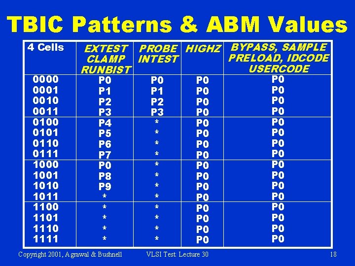
TBIC Patterns & ABM Values 4 Cells 0000 0001 0010 0011 0100 0101 0110 0111 1000 1001 1010 1011 1100 1101 1110 1111 EXTEST PROBE HIGHZ BYPASS, SAMPLE PRELOAD, IDCODE CLAMP INTEST USERCODE RUNBIST P 0 P 1 P 2 P 3 P 4 P 5 P 6 P 7 P 0 P 8 P 9 * * * Copyright 2001, Agrawal & Bushnell P 0 P 1 P 2 P 3 * * * P 0 P 0 P 0 P 0 VLSI Test: Lecture 30 P 0 P 0 P 0 P 0 18

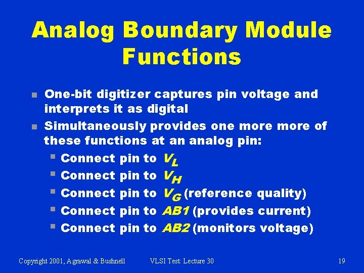
Analog Boundary Module Functions n n One-bit digitizer captures pin voltage and interprets it as digital Simultaneously provides one more of these functions at an analog pin: § Connect pin to VL § Connect pin to VH § Connect pin to VG (reference quality) § Connect pin to AB 1 (provides current) § Connect pin to AB 2 (monitors voltage) Copyright 2001, Agrawal & Bushnell VLSI Test: Lecture 30 19

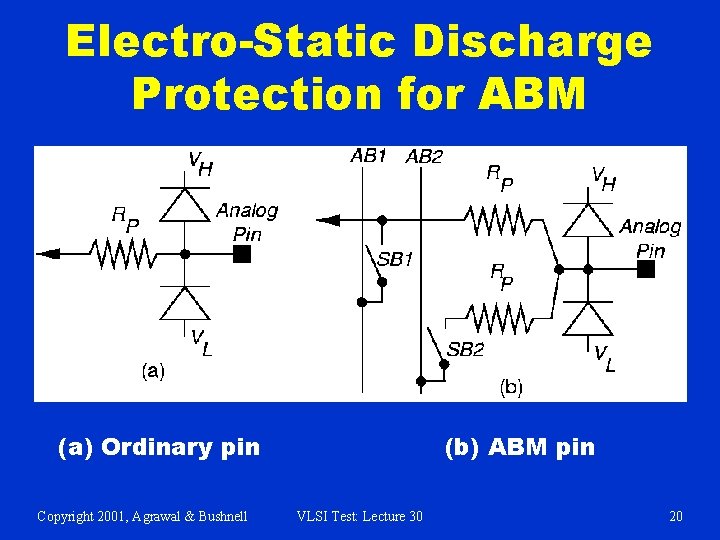
Electro-Static Discharge Protection for ABM (a) Ordinary pin Copyright 2001, Agrawal & Bushnell (b) ABM pin VLSI Test: Lecture 30 20

EXTEST Instruction n Can disable or enable each of these connections for each analog pin: § Core-disconnect state (disconnected from internal analog circuitry) § Connect to VL § Connect to VH Had to be individually pin programmable, because bias voltage pins can never be disconnected, and low impedance R’s or L’s often cannot be disconnected Core-disconnect state often not implemented with a transistor, since that can reduce driver performance Copyright 2001, Agrawal & Bushnell VLSI Test: Lecture 30 21

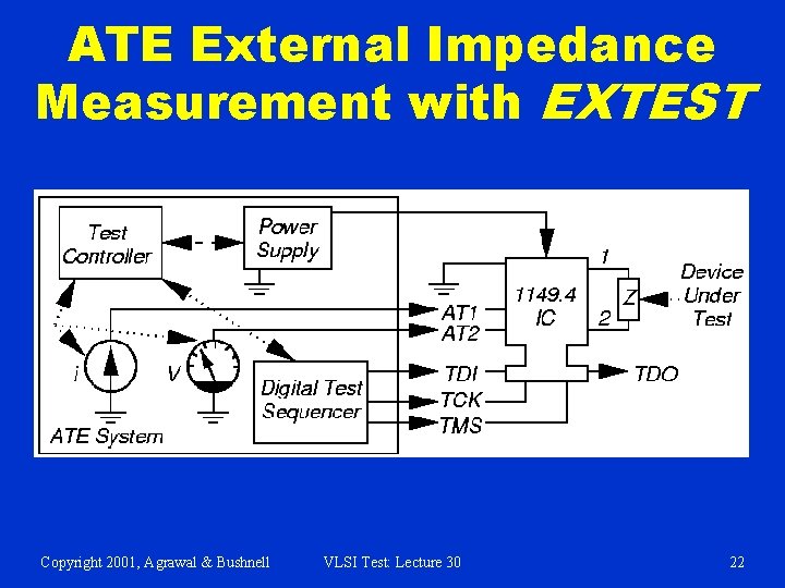
ATE External Impedance Measurement with EXTEST Copyright 2001, Agrawal & Bushnell VLSI Test: Lecture 30 22

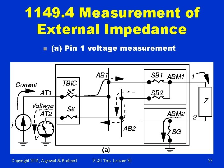
1149. 4 Measurement of External Impedance n (a) Pin 1 voltage measurement Copyright 2001, Agrawal & Bushnell VLSI Test: Lecture 30 23

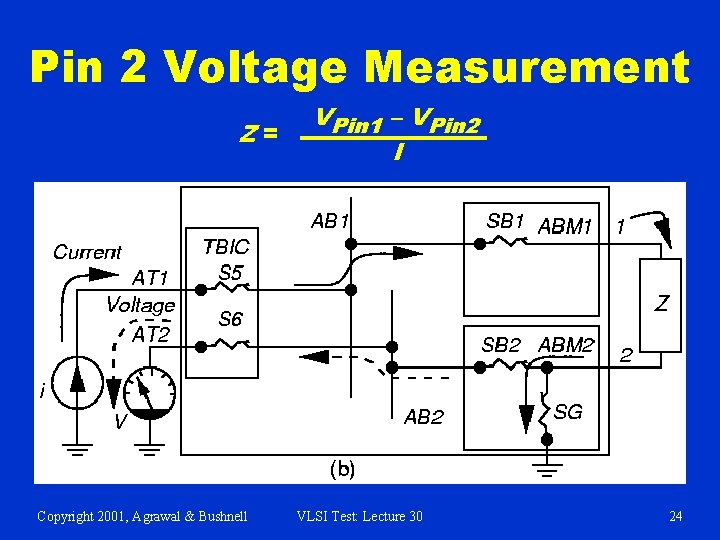
Pin 2 Voltage Measurement Z= Copyright 2001, Agrawal & Bushnell VPin 1 – VPin 2 I VLSI Test: Lecture 30 24

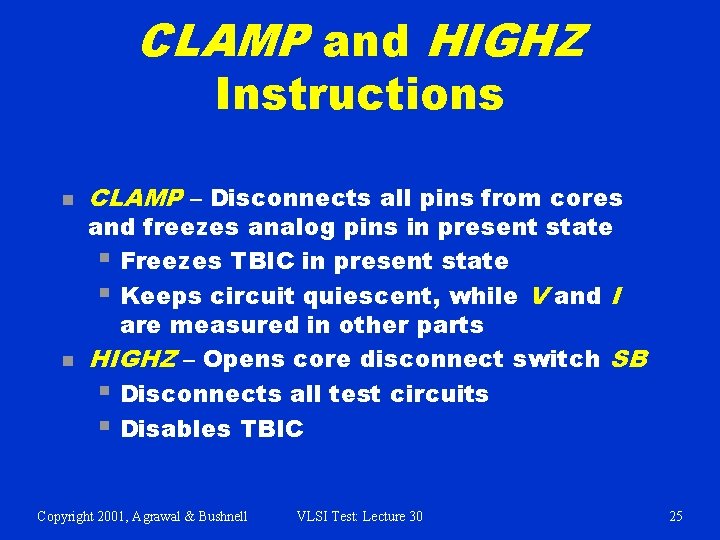
CLAMP and HIGHZ Instructions n n CLAMP – Disconnects all pins from cores and freezes analog pins in present state § Freezes TBIC in present state § Keeps circuit quiescent, while V and I are measured in other parts HIGHZ – Opens core disconnect switch SB § Disconnects all test circuits § Disables TBIC Copyright 2001, Agrawal & Bushnell VLSI Test: Lecture 30 25

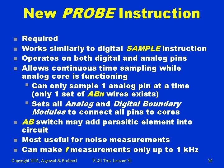
New PROBE Instruction n n n Required Works similarly to digital SAMPLE instruction Operates on both digital and analog pins Allows continuous time sampling while analog core is functioning § Can only sample 1 analog pin at a time (only 1 set of ABn wires exists) § Sets all Analog and Digital Boundary Modules to connect all pins to cores AB switch may add parasitic element into circuit Most useful for noise measurements Can make f measurements only up to 1 k. Hz Copyright 2001, Agrawal & Bushnell VLSI Test: Lecture 30 26

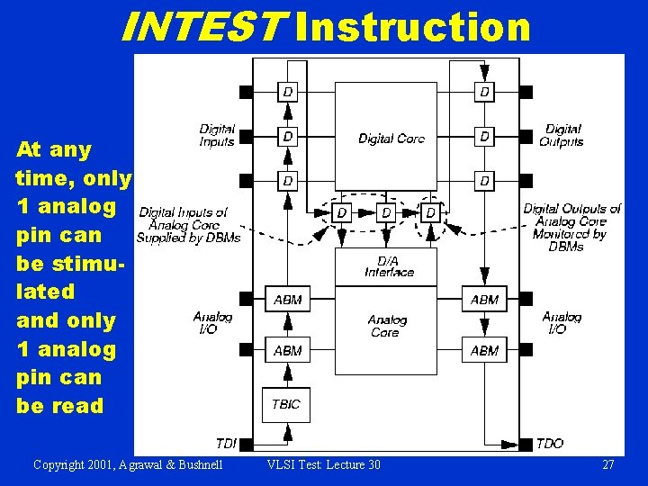
INTEST Instruction At any time, only 1 analog pin can be stimulated and only 1 analog pin can be read Copyright 2001, Agrawal & Bushnell VLSI Test: Lecture 30 27

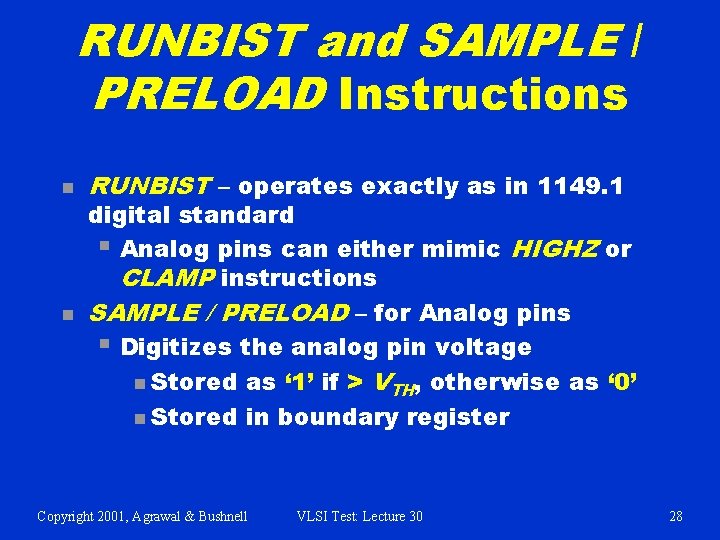
RUNBIST and SAMPLE / PRELOAD Instructions n n RUNBIST – operates exactly as in 1149. 1 digital standard § Analog pins can either mimic HIGHZ or CLAMP instructions SAMPLE / PRELOAD – for Analog pins § Digitizes the analog pin voltage n Stored as ‘ 1’ if > VTH, otherwise as ‘ 0’ n Stored in boundary register Copyright 2001, Agrawal & Bushnell VLSI Test: Lecture 30 28

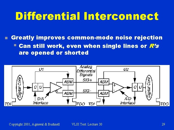
Differential Interconnect n Greatly improves common-mode noise rejection § Can still work, even when single lines or R’s are opened or shorted Copyright 2001, Agrawal & Bushnell VLSI Test: Lecture 30 29

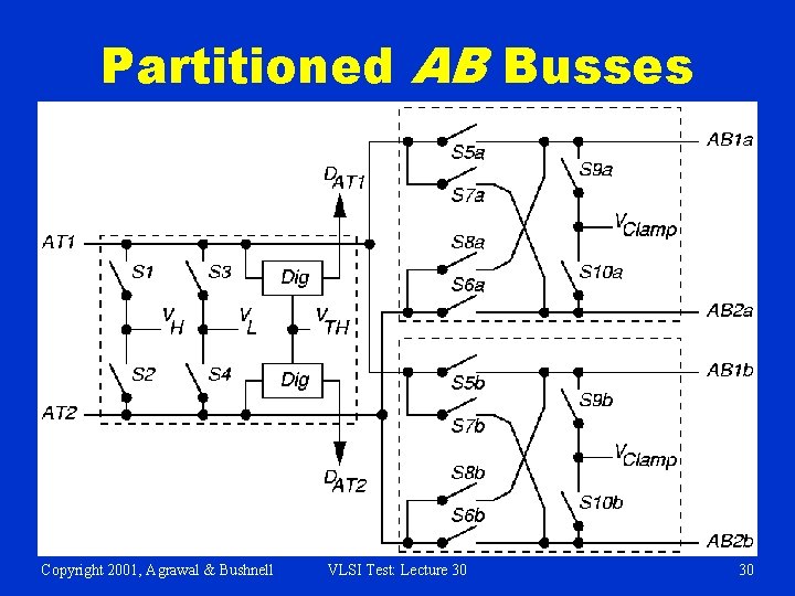
Partitioned AB Busses Copyright 2001, Agrawal & Bushnell VLSI Test: Lecture 30 30

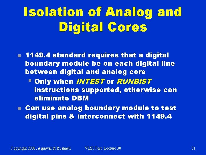
Isolation of Analog and Digital Cores n n 1149. 4 standard requires that a digital boundary module be on each digital line between digital and analog core § Only when INTEST or RUNBIST instructions supported, otherwise can eliminate DBM Can use analog boundary module to test digital pins & interconnect with 1149. 4 Copyright 2001, Agrawal & Bushnell VLSI Test: Lecture 30 31

Analog Switch to Reduce Coupling Copyright 2001, Agrawal & Bushnell VLSI Test: Lecture 30 32

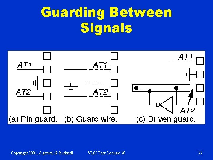
Guarding Between Signals Copyright 2001, Agrawal & Bushnell VLSI Test: Lecture 30 33

Summary n n n Analog test bus allows static analog tests Non-static or feedback circuits are hard to test Good for locating shorts, opens, and wrong external component values § VH and VL switches in ABM must be able to survive large voltage differences Needs customizing digitizing receiver for digitizing analog bus – inverter not suitable Can eliminate separate process monitor transistors and resistors on wafers – saves area Needs large, low-resistance transistor switches to avoid common mode measurement errors Copyright 2001, Agrawal & Bushnell VLSI Test: Lecture 30 34