Lecture 3 Thermal Process OBJECTIVES Identify types of
Lecture 3 Thermal Process
OBJECTIVES Identify types of thermal process Ability to describe, explain and discuss on oxidation (wet and dry oxidation and include cleaning process) Ability to describe Diffusion and Drive-in, Annealing, Rapid thermal process (RTP).
Definition • Thermal processes are the processes operate at high temperature, which is usually higher than melting point of aluminum (660. 3°C). • The process grows a layer of silicon dioxide to protect the silicon surface. • The silicon dioxide layer is a very stable and strong dielectric.
• One of the advantages of silicon wafer is the high temperature process capability. The examples of the high temperature process are oxidation, diffusion, deposition and annealing which involves temperature between 700°C to 1200°C.
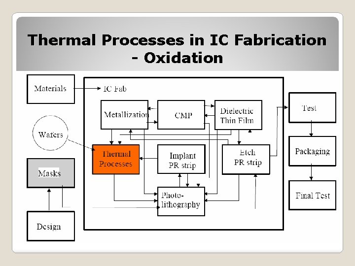
Thermal Processes in IC Fabrication - Oxidation
Furnace • There are 2 types of furnace; horizontal and vertical. Both of the furnaces require stable, uniform and accurate temperature control, low particulate contamination, high productivity and reliability. Normally consists of 5 basic components; control system, process tube, gas delivery system, exhaust system and loading system.
Horizontal Furnace • Commonly used tool for thermal processes • Often be called as diffusion furnace • Quartz tube inside a ceramic liner called muffle • Multi-tube system
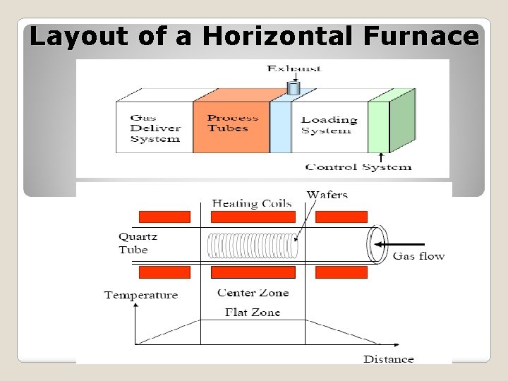
Layout of a Horizontal Furnace
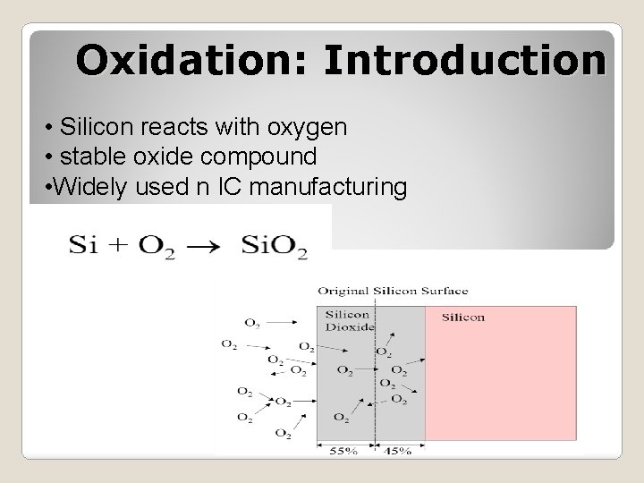
Oxidation: Introduction • Silicon reacts with oxygen • stable oxide compound • Widely used n IC manufacturing
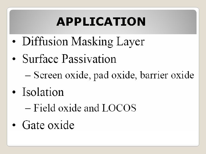
APPLICATION
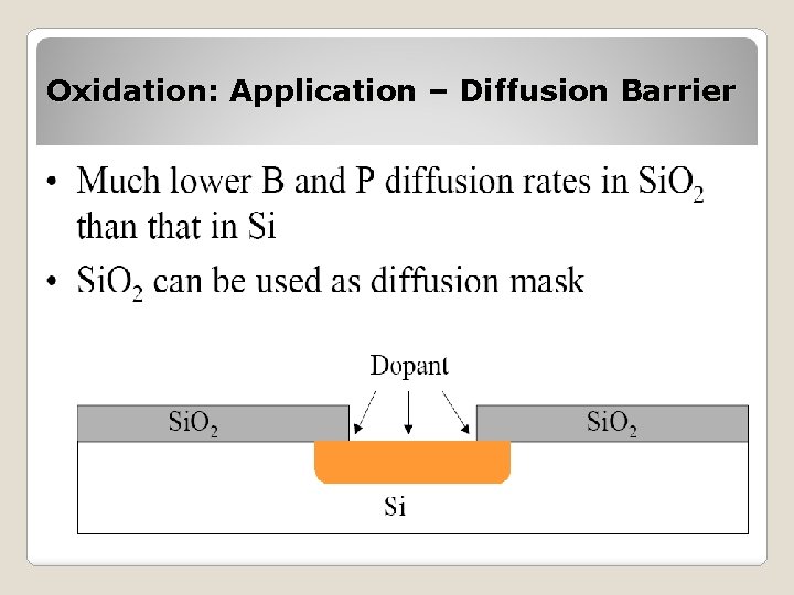
Oxidation: Application – Diffusion Barrier
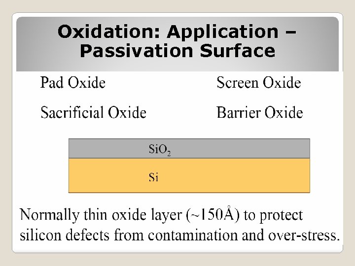
Oxidation: Application – Passivation Surface
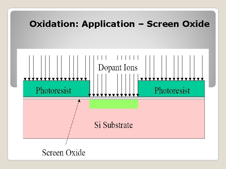
Oxidation: Application – Screen Oxide
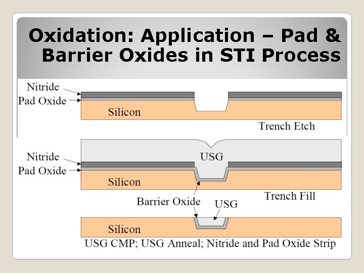
Oxidation: Application – Pad & Barrier Oxides in STI Process
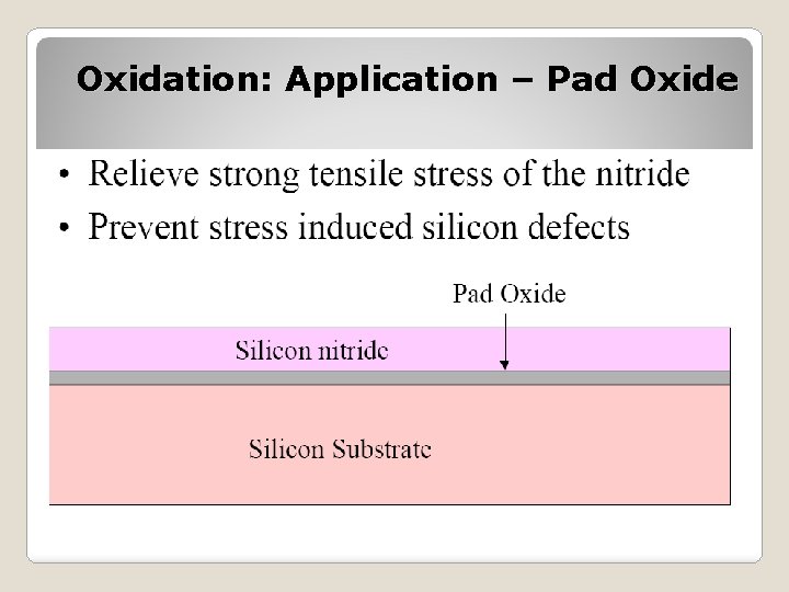
Oxidation: Application – Pad Oxide
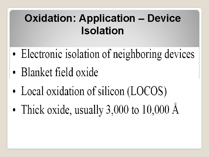
Oxidation: Application – Device Isolation
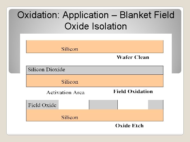
Oxidation: Application – Blanket Field Oxide Isolation
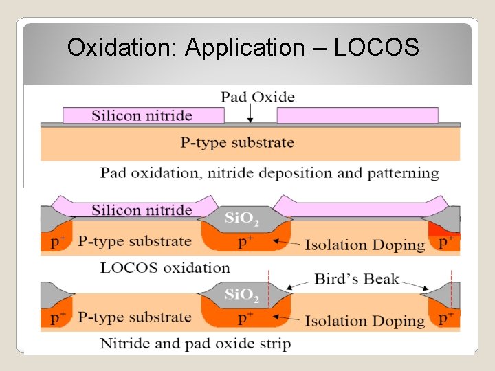
Oxidation: Application – LOCOS
LOCOS, short for LOCal Oxidation of Silicon, is a microfabrication process where silicon dioxide is formed in selected areas on a silicon wafer having the Si. O 2 interface at a lower point than the rest of the silicon surface. This technology was developed to insulate MOS transistors from each other. The main goal is to create a silicon oxide insulating structure that penetrates under the surface of the wafer
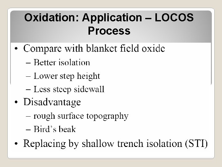
Oxidation: Application – LOCOS Process
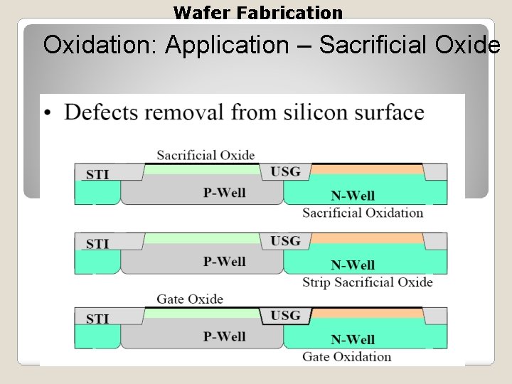
Wafer Fabrication Oxidation: Application – Sacrificial Oxide
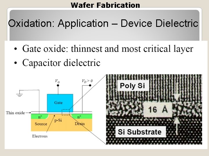
Wafer Fabrication Oxidation: Application – Device Dielectric
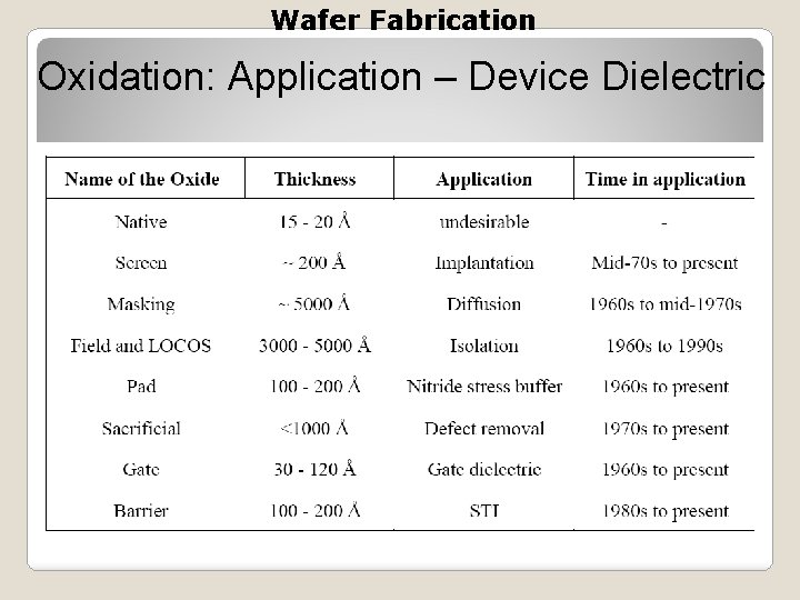
Wafer Fabrication Oxidation: Application – Device Dielectric
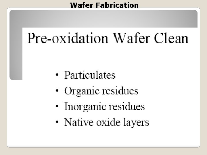
Wafer Fabrication
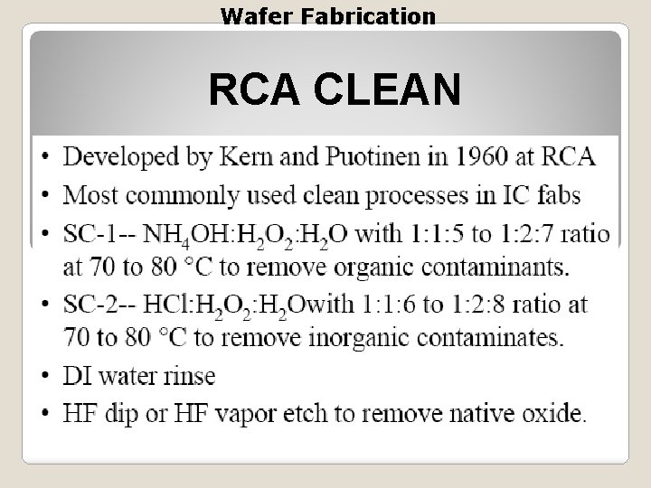
Wafer Fabrication RCA CLEAN
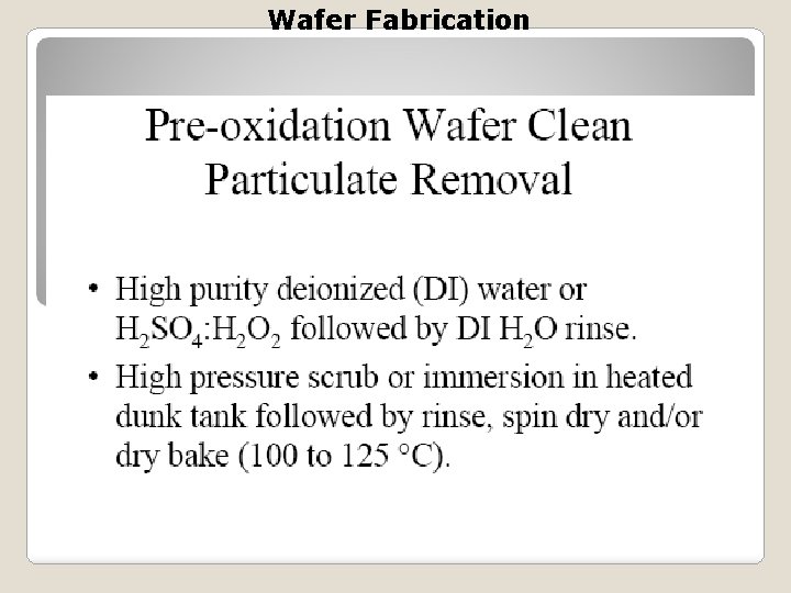
Wafer Fabrication
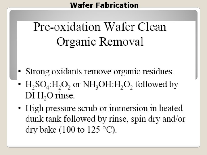
Wafer Fabrication
Wafer Fabrication
Wafer Fabrication
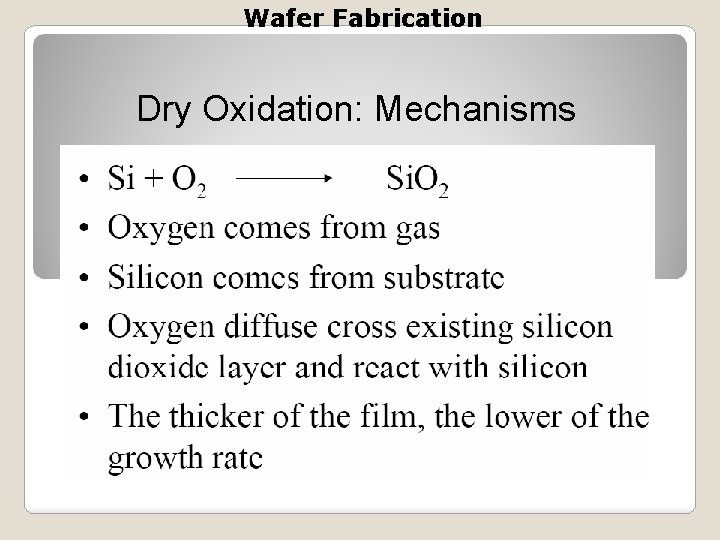
Wafer Fabrication Dry Oxidation: Mechanisms
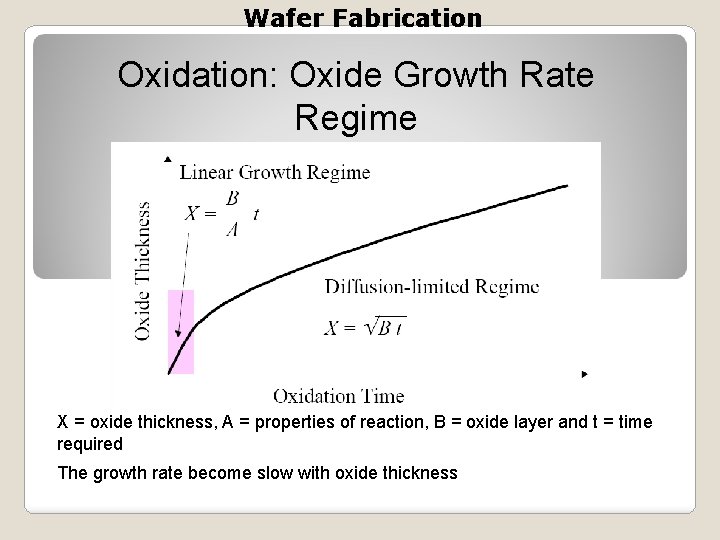
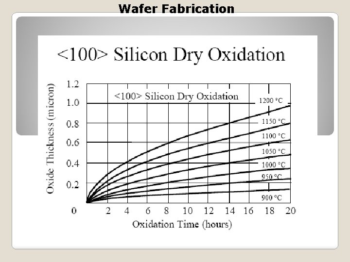
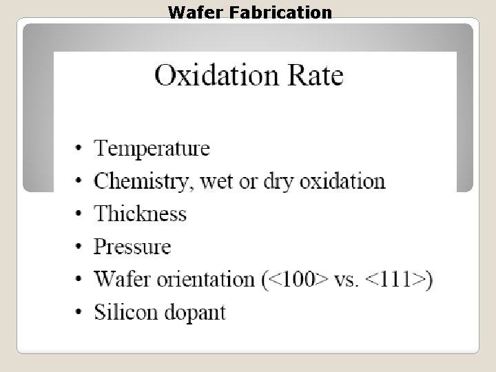
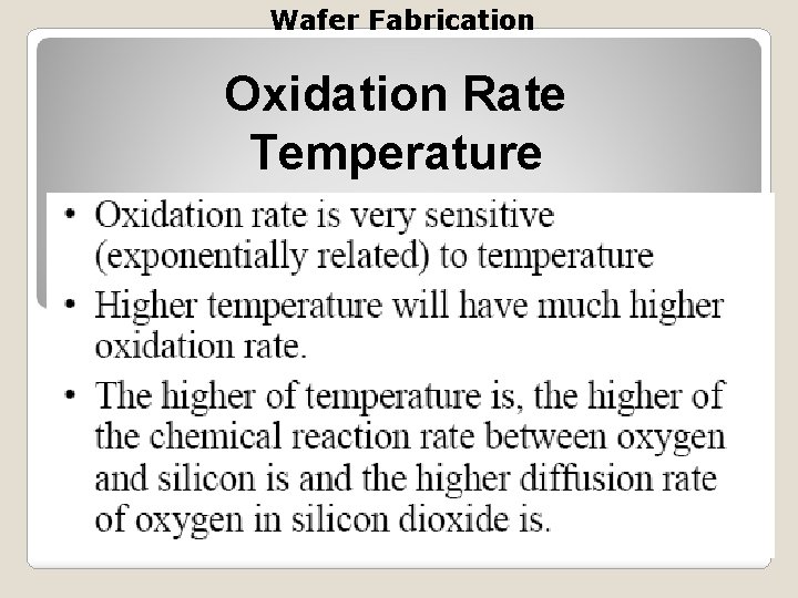
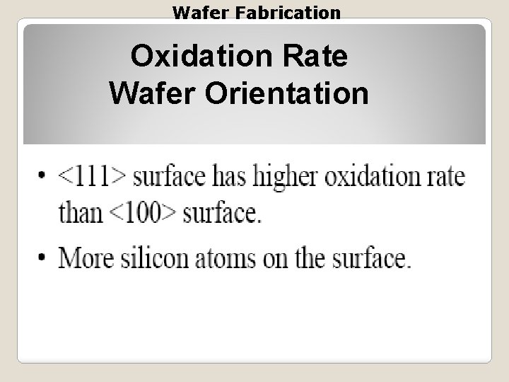
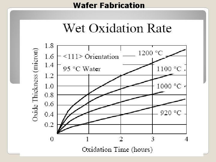
Wafer Fabrication Oxidation: Oxide Growth Rate Regime X = oxide thickness, A = properties of reaction, B = oxide layer and t = time required The growth rate become slow with oxide thickness
Wafer Fabrication Oxidation: Oxide Growth Rate Regime • When oxide has just started to grow and the oxide layer is very this (< 500 A native oxide) , oxygen molecules can penetrate the oxide with a few collision in the oxide layer and reach the silicon, to react and continue to grow the silicon dioxide film. This is called the linear growth regime ( linearly increasing with growth time). • When the oxide film becomes thicker, oxygen molecules can no longer pass through the oxide layer without many collisions with the atoms inside the oxide film. They have to diffuse across the growing oxide to reach silicon and react with it to form silicon dioxide. This is called the diffusision-limited regime (growth rate is slower than linear).
Wafer Fabrication
Wafer Fabrication
Wafer Fabrication
Wafer Fabrication
Wafer Fabrication Oxidation Rate Temperature
Wafer Fabrication Oxidation Rate Wafer Orientation
Wafer Fabrication
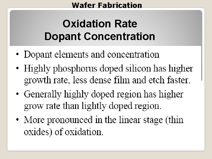
Wafer Fabrication Oxidation Rate Dopant Concentration
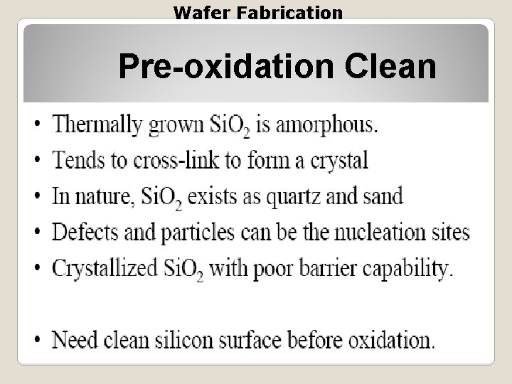
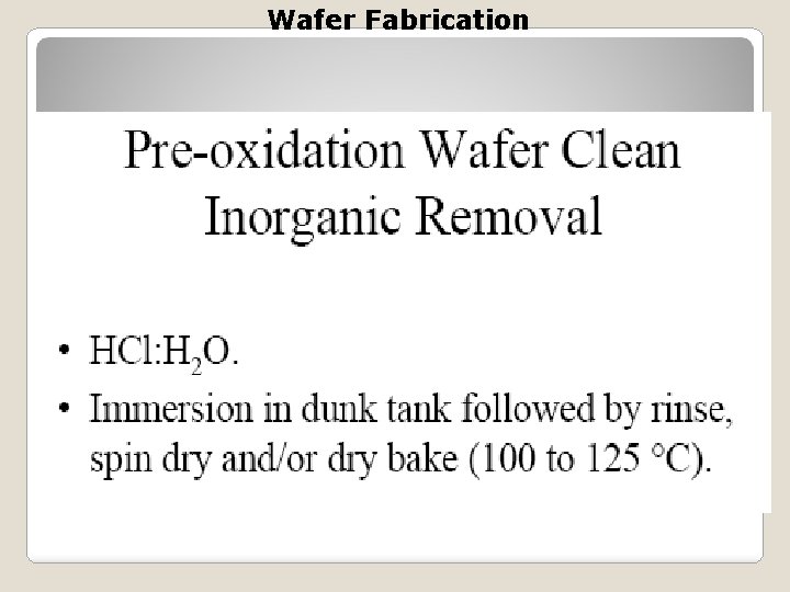
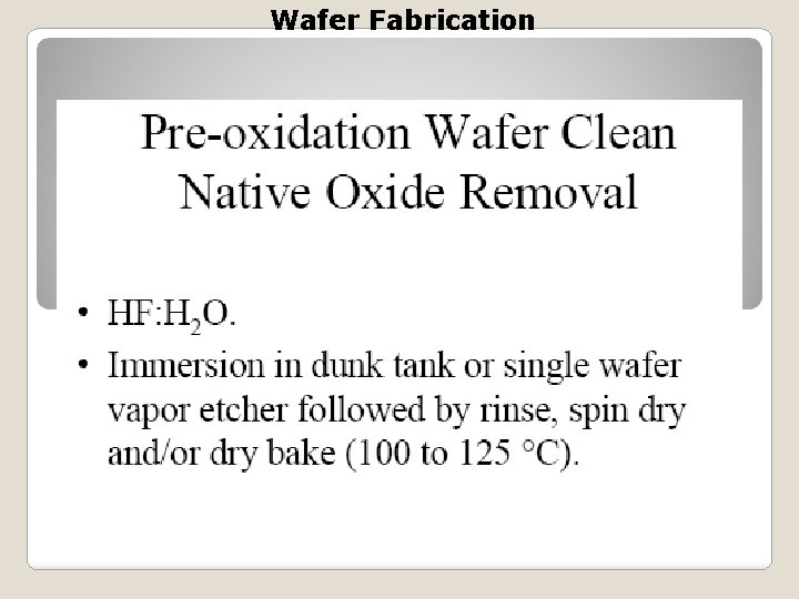
Wafer Fabrication Pre-oxidation Clean
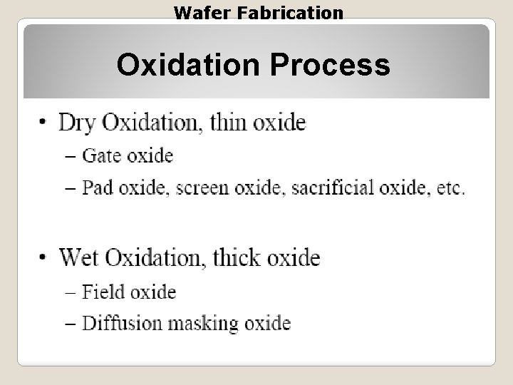
Wafer Fabrication Oxidation Process
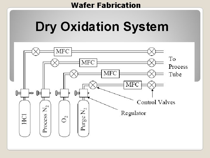
Wafer Fabrication Dry Oxidation System
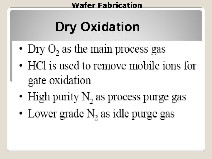
Wafer Fabrication Dry Oxidation
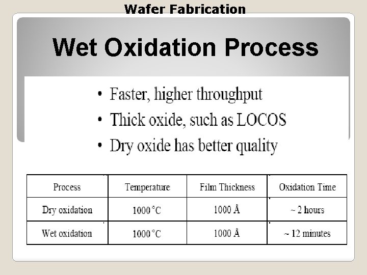
Wafer Fabrication Wet Oxidation Process
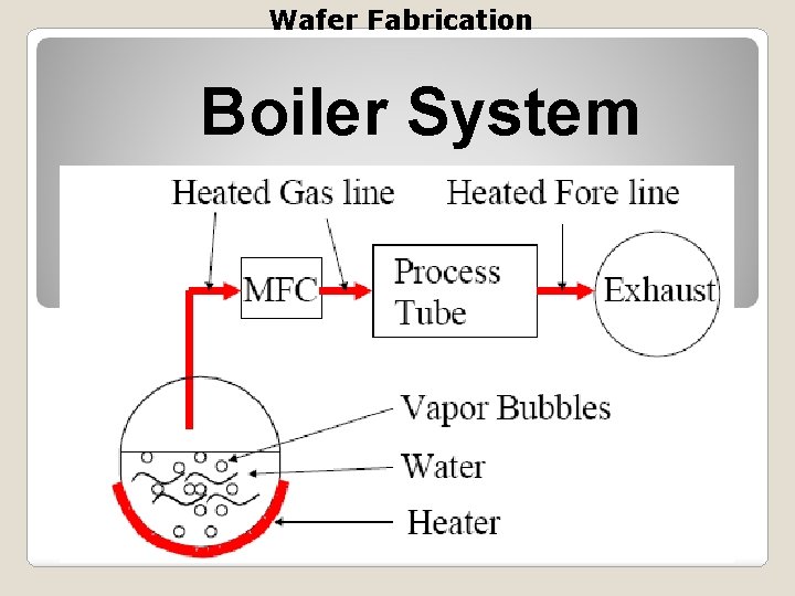
Wafer Fabrication Boiler System
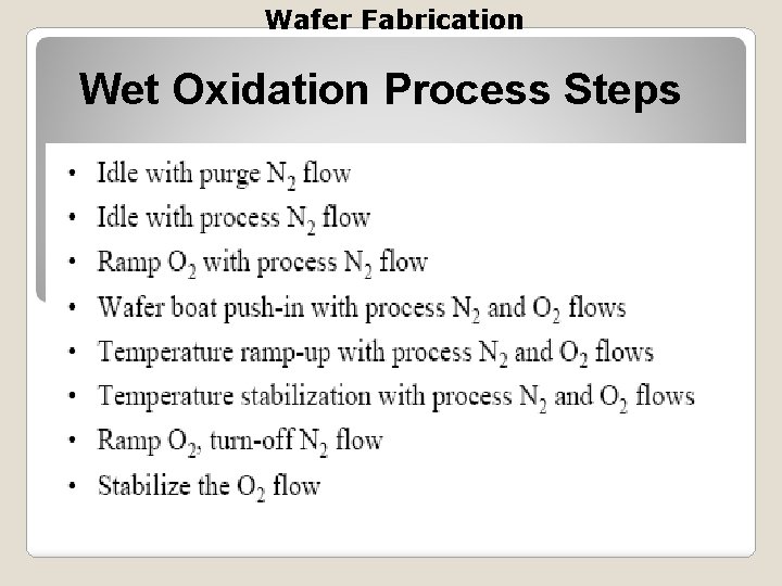
Wafer Fabrication Wet Oxidation Process Steps
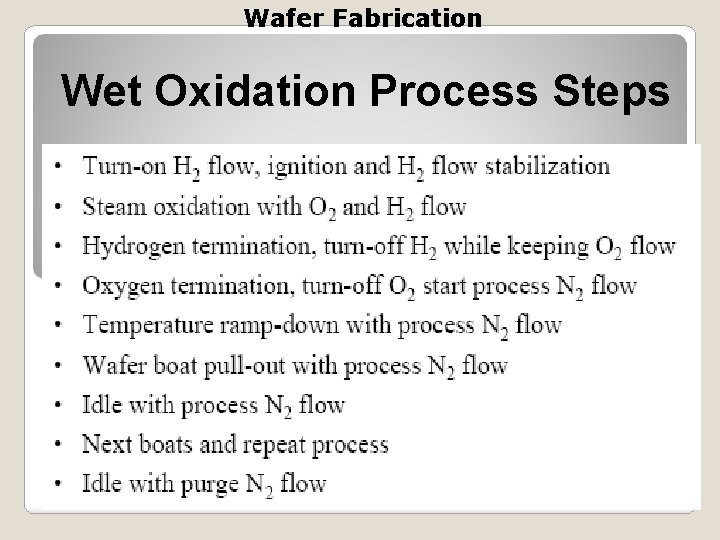
Wafer Fabrication Wet Oxidation Process Steps
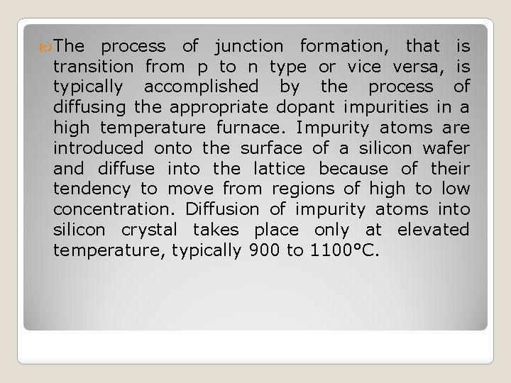
The process of junction formation, that is transition from p to n type or vice versa, is typically accomplished by the process of diffusing the appropriate dopant impurities in a high temperature furnace. Impurity atoms are introduced onto the surface of a silicon wafer and diffuse into the lattice because of their tendency to move from regions of high to low concentration. Diffusion of impurity atoms into silicon crystal takes place only at elevated temperature, typically 900 to 1100°C.
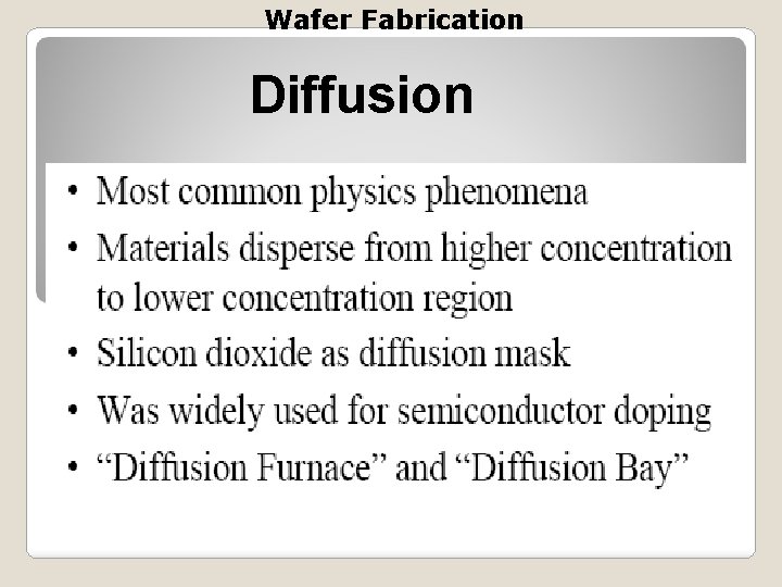
Wafer Fabrication Diffusion
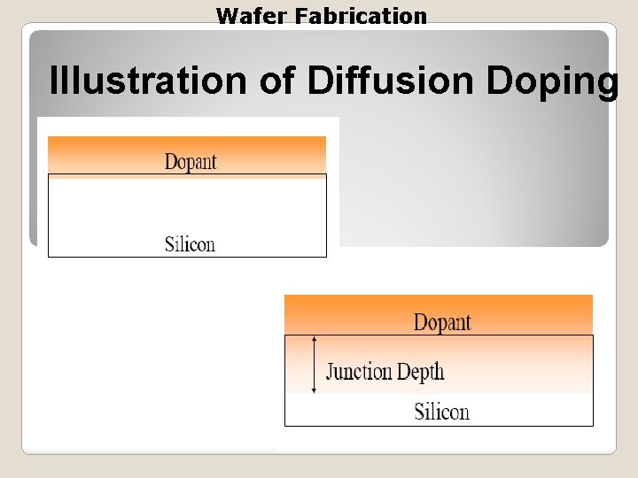
Wafer Fabrication Illustration of Diffusion Doping
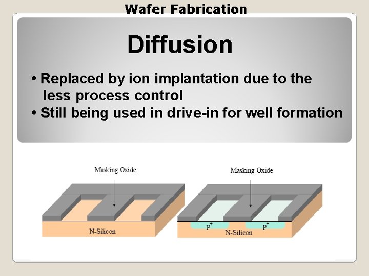
Wafer Fabrication Diffusion • Replaced by ion implantation due to the less process control • Still being used in drive-in for well formation
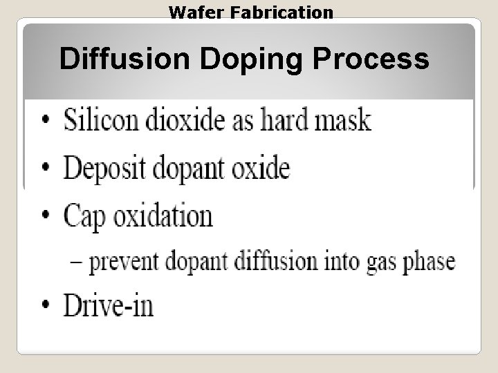
Wafer Fabrication Diffusion Doping Process
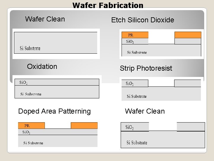
Wafer Fabrication Wafer Clean Oxidation Doped Area Patterning Etch Silicon Dioxide Strip Photoresist Wafer Clean
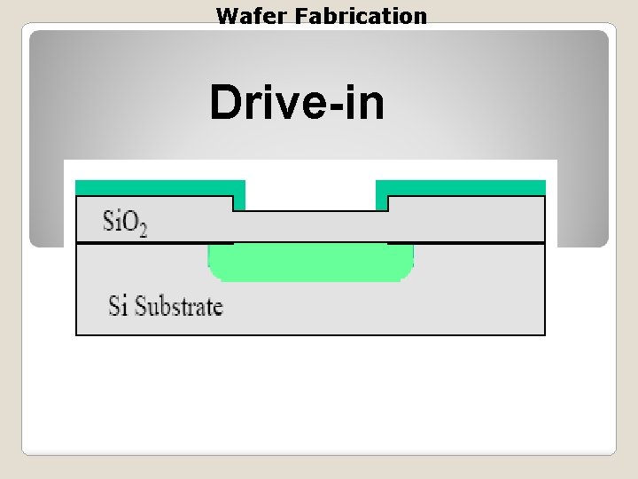
Wafer Fabrication Drive-in
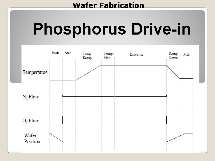
Wafer Fabrication Phosphorus Drive-in
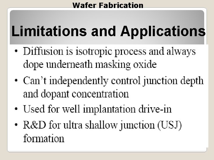
Wafer Fabrication Limitations and Applications
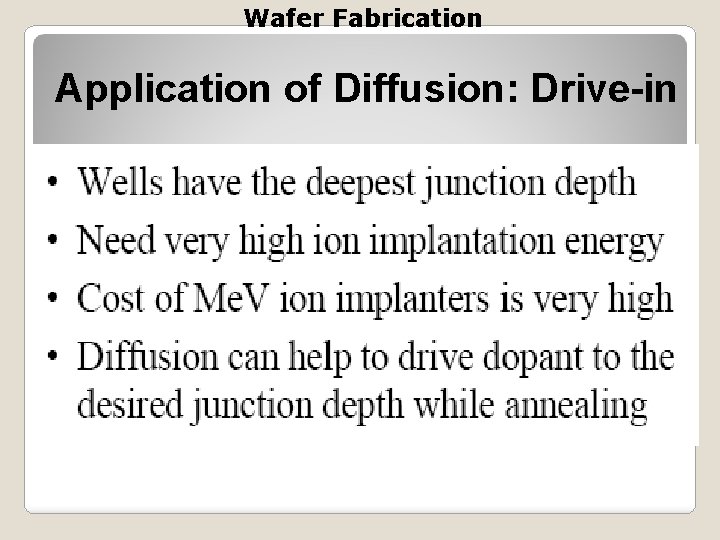
Wafer Fabrication Application of Diffusion: Drive-in
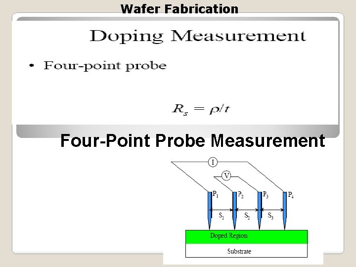
Wafer Fabrication Four-Point Probe Measurement
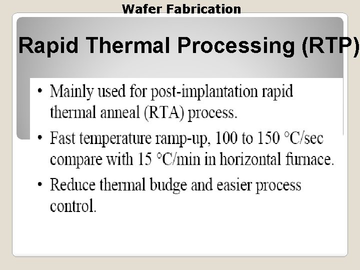
Wafer Fabrication Rapid Thermal Processing (RTP)
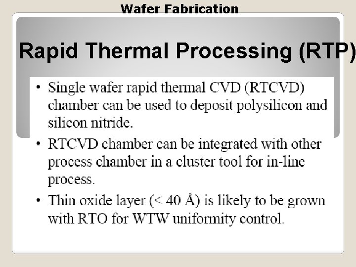
Wafer Fabrication Rapid Thermal Processing (RTP)
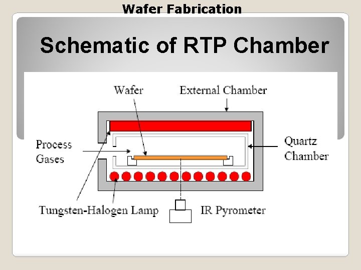
Wafer Fabrication Schematic of RTP Chamber
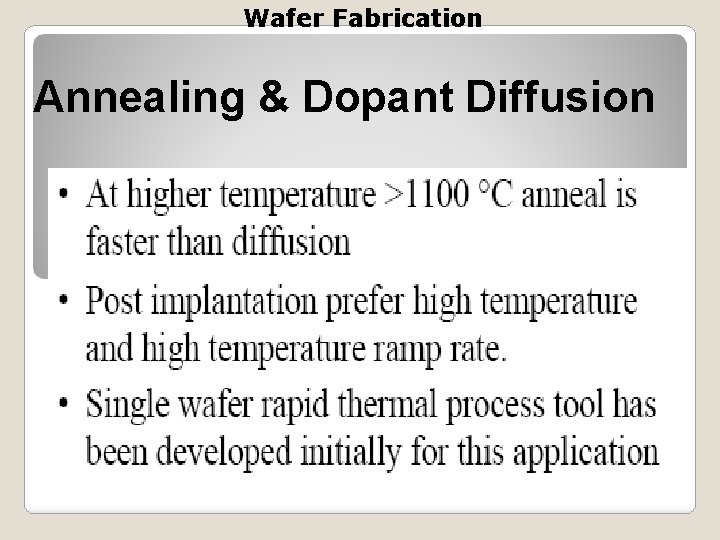
Wafer Fabrication Annealing & Dopant Diffusion
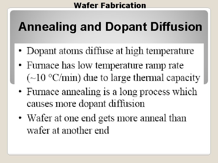
Wafer Fabrication Annealing and Dopant Diffusion
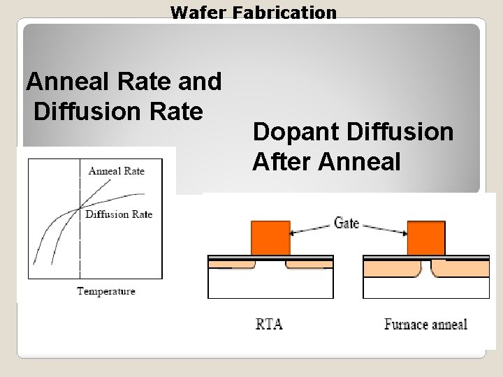
Wafer Fabrication Anneal Rate and Diffusion Rate Dopant Diffusion After Anneal
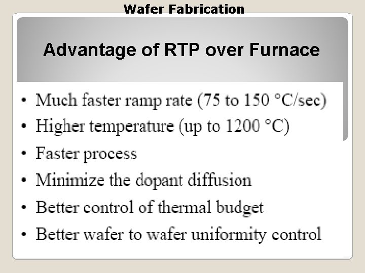
Wafer Fabrication Advantage of RTP over Furnace
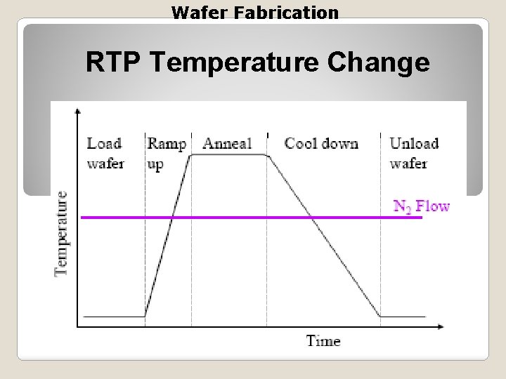
Wafer Fabrication RTP Temperature Change
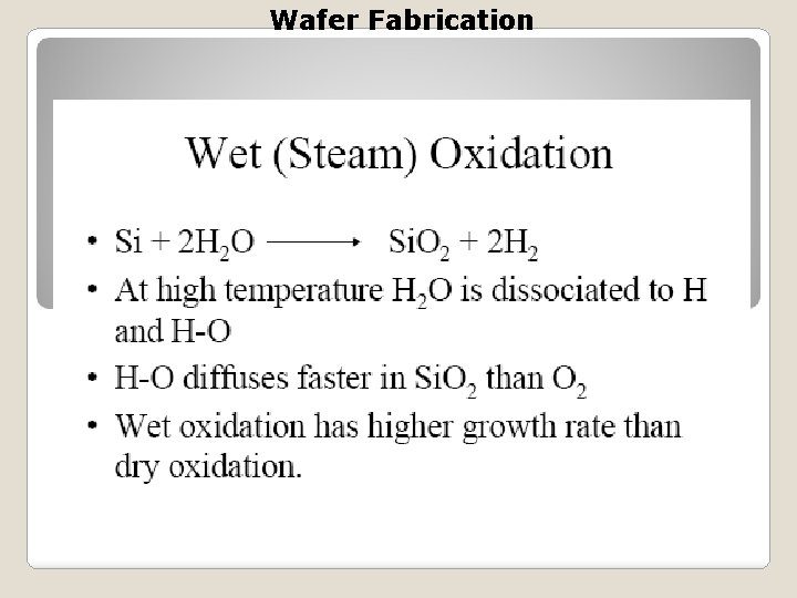
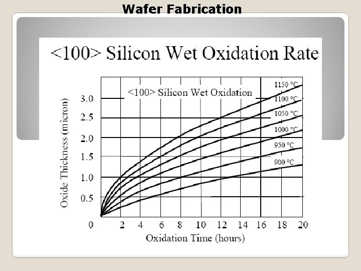
Wafer Fabrication Summary of Thermal Process 1. Oxidation, diffusion, annealing, and deposition 2. Wet oxidation is faster, dry oxidation has better film quality. Advanced fab: mainly dry oxidation. 3. Diffusion doping with oxide mask, used in lab 4. Annealing recovers crystal and activates dopants 5. RTP: better control, faster and less diffusion 6. Furnaces: high throughput and low cost, will continue to be used in the future fabs
- Slides: 69