LECTURE 3 LOGIC GATES SWITCHING CIRCUITS BOOLEAN ALGEBRA
LECTURE 3: LOGIC GATES & SWITCHING CIRCUITS & BOOLEAN ALGEBRA Engr. Muhammad Saad. Ullah
OUT LINE • Lecture 2 remaining Topic (Binary Codes, Binary Logic) • Switching Circuits • Logic Gates ( AND, OR, NOT, NAND, NOR, XNOR) • Logic Circuits / Combinational logic circuits • Introduction to Boolean algebra • Question & Answers 2
BINARY CODES Digital systems use signals that have two distinct values and circuit elements that have two stable states A binary number of n digits, for example, may be represented by n binary circuit elements, each having an output signal equivalent to 0 or 1. the codes must be in binary because, in today’s technology, only circuits that represent and manipulate patterns of 0’s and 1’s can be manufactured economically for use in computers. 3
BINARY CODES • An n‐bit binary code is a groupn bits of that assumes up to 2 n distinct combinations of 1’s and 0’s, with each combination representing one element of the set that is being coded. • A set of four elements can be coded with two bits, with each element assigned one of the following bit combinations: 00, 01, 10, 11. • The bit combination of an n‐bit code is determined from the count in binary fromn -01 to 2 4
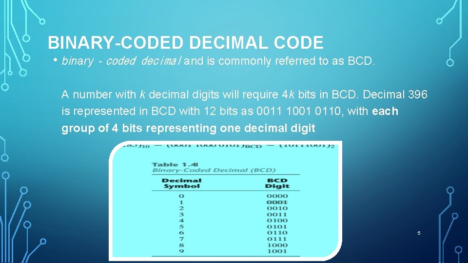
BINARY-CODED DECIMAL CODE • binary‐coded decimal and is commonly referred to as BCD. A number with k decimal digits will require 4 k bits in BCD. Decimal 396 is represented in BCD with 12 bits as 0011 1001 0110, with each group of 4 bits representing one decimal digit 5
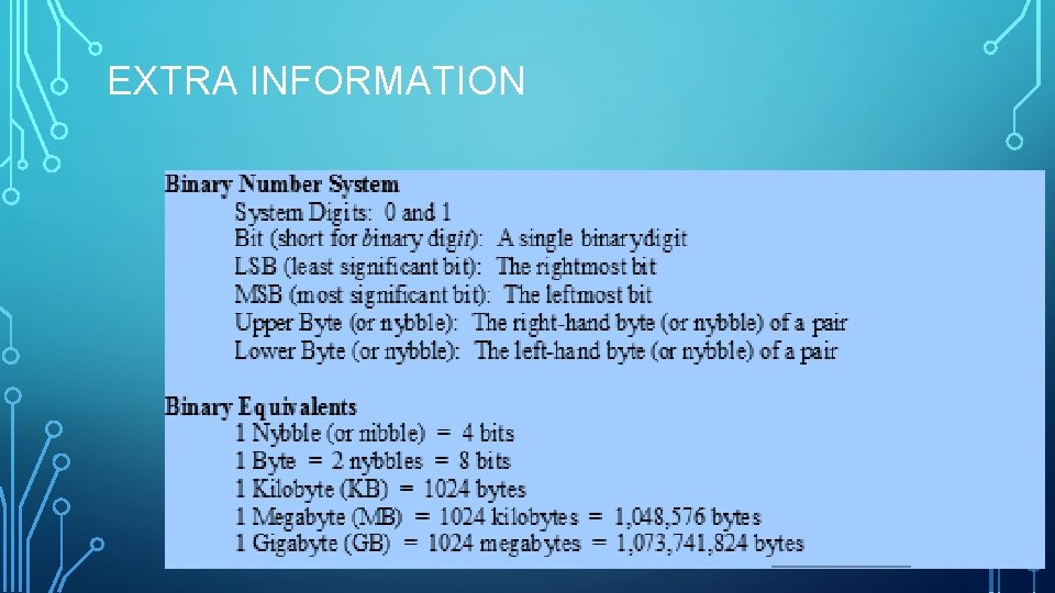
EXTRA INFORMATION
BINARY STORAGE AND REGISTERS • A binary cell is a device that possesses two stable states and is capable of storing one bit (0 or 1) of information • • Registers • • • Tuple A register is a group of binary cells. A register In mathematics, an n-tuple is a sequence (or with n cells can store any discrete quantity of ordered list) of n elements, where n is a nonnegative integer. There is only one 0 -tuple, an information that contains n bits. The state of a register is an n‐tuple of 1’s and 0’s, with eachempty sequence. An n-tuple is defined inductively using the construction of an ordered bit designating the state of one cell in the pair. register. Consider, for example, a 16‐bit register with the following binary content: 1100001111001001 The device most commonly used for holding data is a register 7
B I NARY LOGIC • Binary logic deals with variables that take on two discrete values (logical meaning). • The two values the variables assume may be called by different names (true and false, yes and no but it is convenient to think in terms of bits and assign the values 1 and 0). • Definition of Binary Logic • Binary logic consists of binary variables and a set of logical operations. • The variables are designated by letters of the alphabet, such as A, B, C, x, y, z, etc. with each variable having two and only two distinct possible values: 1 and 0. • There are three basic logical operations: AND, OR, and NOT. Each operation produces a binary result, denoted by z. • AND and OR are the same as those used for multiplication and addition. 8
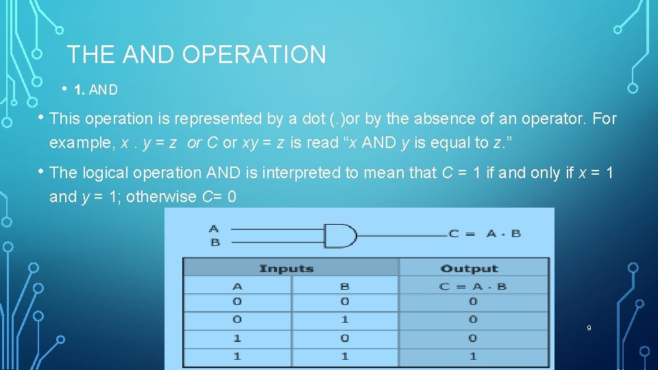
THE AND OPERATION • 1. AND • This operation is represented by a dot (. )or by the absence of an operator. For example, x. y = z or C or xy = z is read “x AND y is equal to z. ” • The logical operation AND is interpreted to mean that C = 1 if and only if x = 1 and y = 1; otherwise C= 0 9
THE OR & NOT OPERATION • 2. The OR Operation • This operation is represented by a plus sign. For example, x + y = z is read “x OR y is equal to z, ” meaning that z = 1 if x = 1 or if y = 1 or if both x = 1 and y = 1. If both x = 0 and y = 0, then z = 0. • 3. NOT: • This operation is represented by a prime (sometimes by an overbar). For example, x/ = z (or x– = z) is read “not x is equal to z, ” meaning that z is what x is not. In other words, if x = 1, then z = 0, but if x = 0, then z = 1. The NOT operation is also referred to as the complement operation, since it changes 10 a 1 to 0 and a 0 to 1.
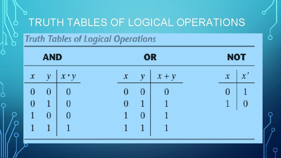
TRUTH TABLES OF LOGICAL OPERATIONS 11
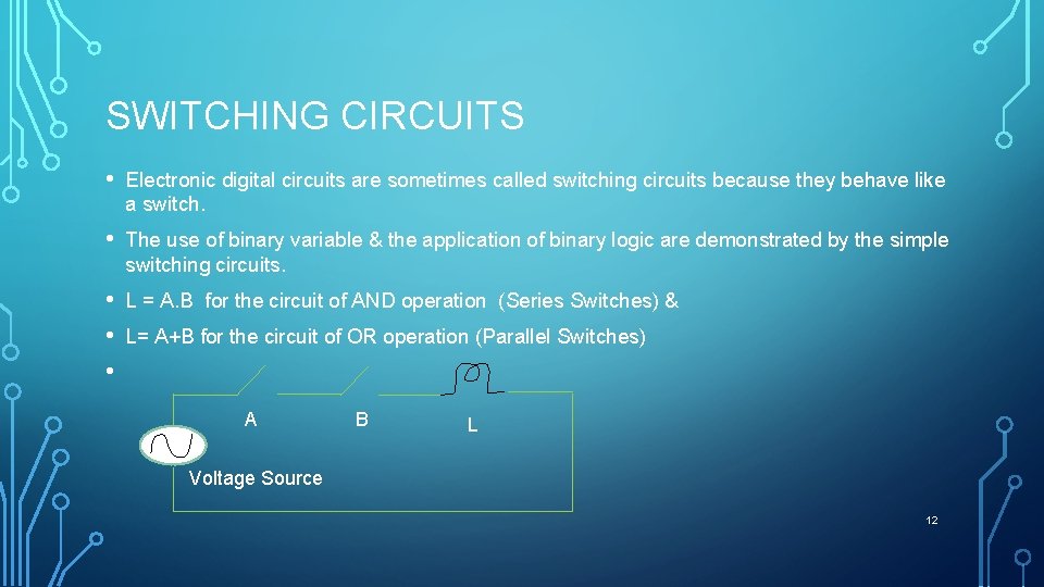
SWITCHING CIRCUITS • Electronic digital circuits are sometimes called switching circuits because they behave like a switch. • The use of binary variable & the application of binary logic are demonstrated by the simple switching circuits. • • • L = A. B for the circuit of AND operation (Series Switches) & L= A+B for the circuit of OR operation (Parallel Switches) A B L Voltage Source 12
LOGIC GATES DEFINITI ON: • A logic gate is a an electronics circuit which makes logic decision. • In other words • “ A logic gate is an electronic circuit having one or more inputs and only one output which will be either high or low (based on the input status) • Logic gates are electronic circuits that operate on one or more input signals to produce an output signal • Logic gates are widely used in digital computers and in different types of system and circuits. 13
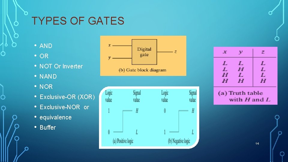
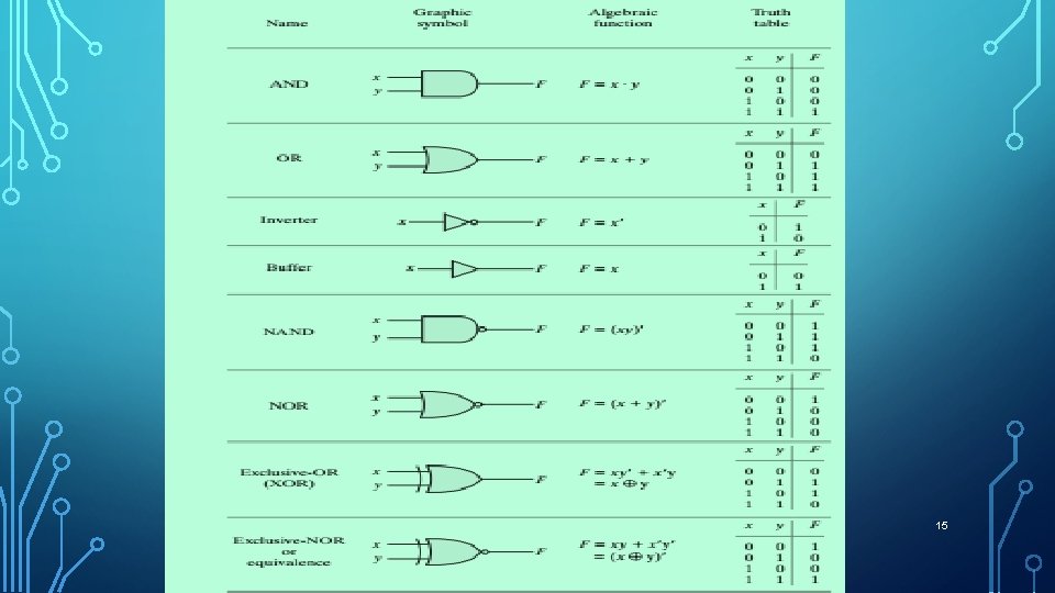
TYPES OF GATES • • • AND OR NOT Or Inverter NAND NOR Exclusive-OR (XOR) Exclusive-NOR or equivalence Buffer 14
15
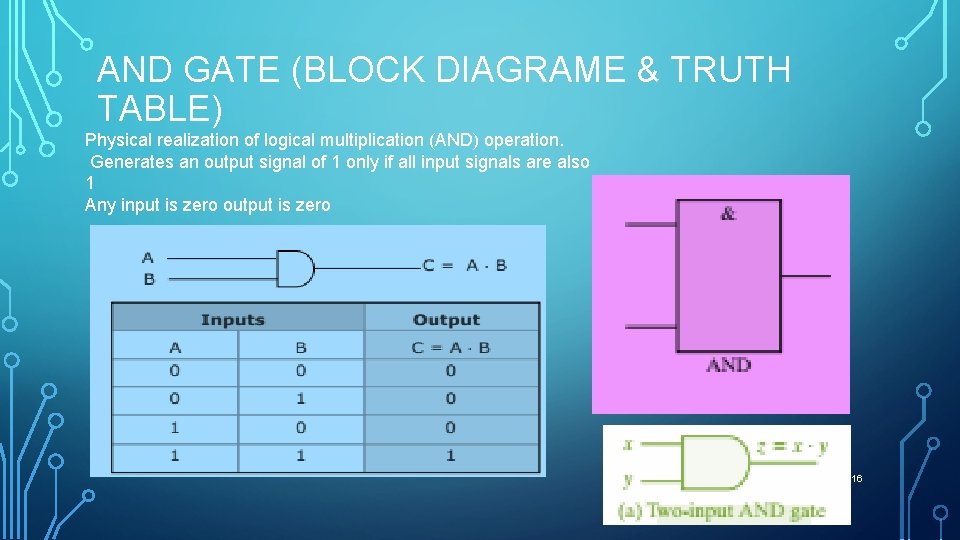
AND GATE (BLOCK DIAGRAME & TRUTH TABLE) Physical realization of logical multiplication (AND) operation. Generates an output signal of 1 only if all input signals are also 1 Any input is zero output is zero 16
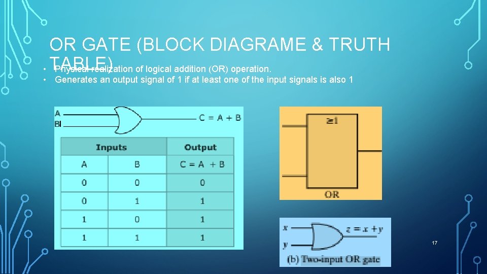
OR GATE (BLOCK DIAGRAME & TRUTH • TABLE) Physical realization of logical addition (OR) operation. • Generates an output signal of 1 if at least one of the input signals is also 1 17
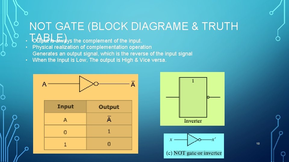
NOT GATE (BLOCK DIAGRAME & TRUTH • TABLE) Output is always the complement of the input. • Physical realization of complementation operation Generates an output signal, which is the reverse of the input signal • When the Input is Low, The output is High & Vice versa. 18
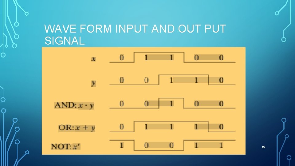
WAVE FORM INPUT AND OUT PUT SIGNAL 19
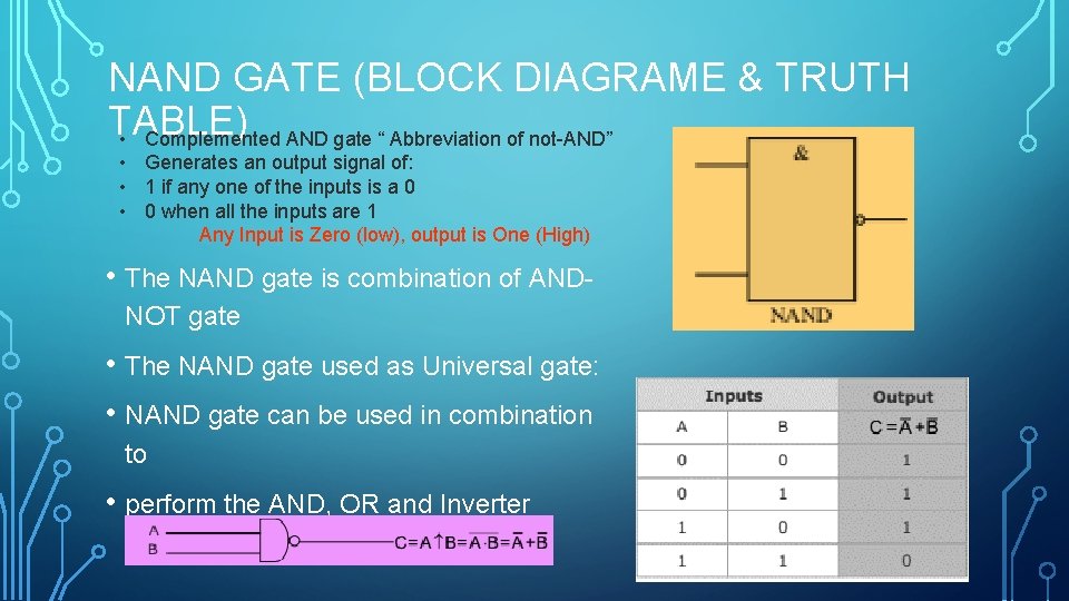
NAND GATE (BLOCK DIAGRAME & TRUTH TABLE) • Complemented AND gate “ Abbreviation of not-AND” • Generates an output signal of: • 1 if any one of the inputs is a 0 • 0 when all the inputs are 1 Any Input is Zero (low), output is One (High) • The NAND gate is combination of ANDNOT gate • The NAND gate used as Universal gate: • NAND gate can be used in combination to • perform the AND, OR and Inverter Operation. 20
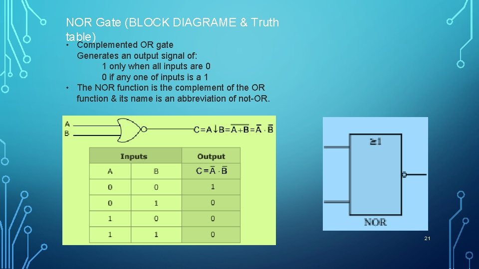
NOR Gate (BLOCK DIAGRAME & Truth table) • Complemented OR gate Generates an output signal of: 1 only when all inputs are 0 0 if any one of inputs is a 1 • The NOR function is the complement of the OR function & its name is an abbreviation of not-OR. 21
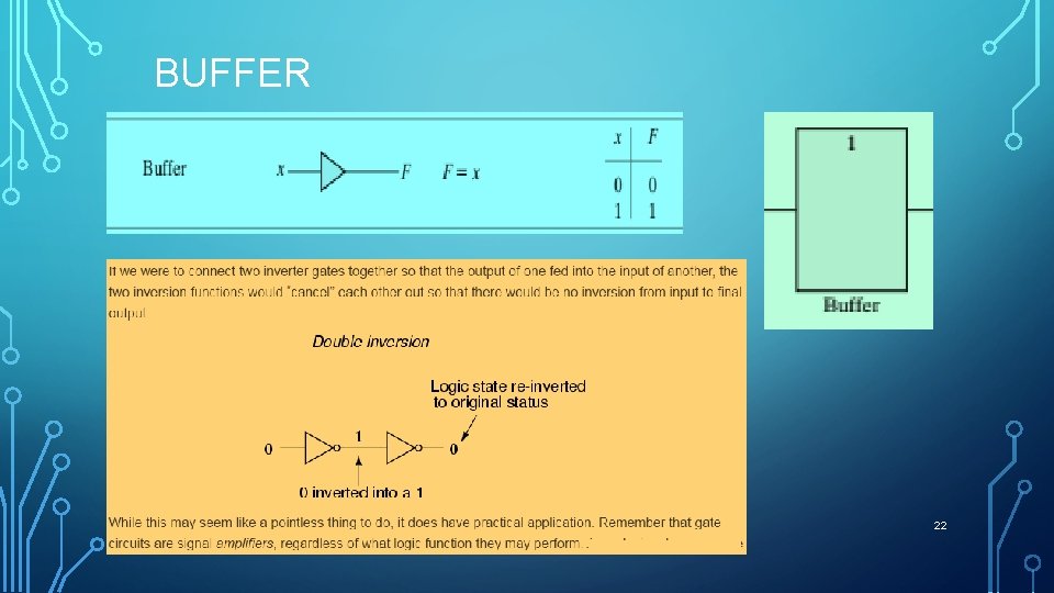
BUFFER 22
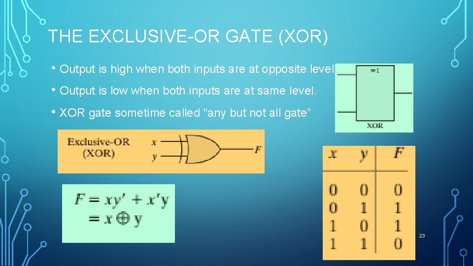
THE EXCLUSIVE-OR GATE (XOR) • Output is high when both inputs are at opposite level • Output is low when both inputs are at same level. • XOR gate sometime called “any but not all gate” or 23
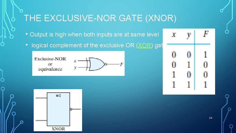
THE EXCLUSIVE-NOR GATE (XNOR) • Output is high when both inputs are at same level • logical complement of the exclusive OR (XOR) gate 24
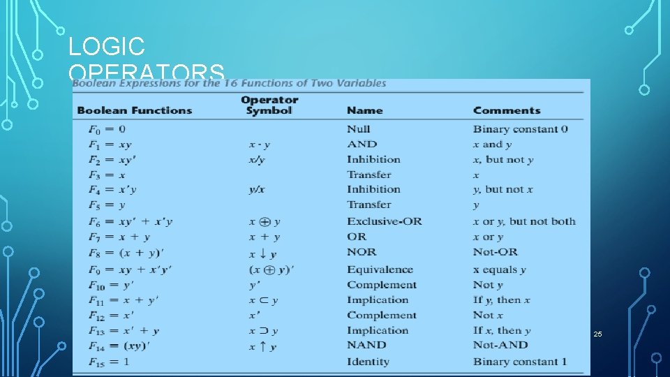
LOGIC OPERATORS 25
LOGIC CIRCUITS/ COMBINATIONAL LOGIC CIRCUITS • When logic gates are interconnected to form a gating / logic network, it is known as a combinational logic circuit. The Boolean algebra expression for a given logic circuit can be derived by systematically progressing from input to output on the gates. • The three logic gates (AND, OR, and NOT) are logically complete because any Boolean expression can be realized as a logic circuit using only these three gate 26
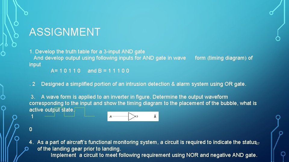
ASSIGNMENT 1. Develop the truth table for a 3 -input AND gate And develop output using following inputs for AND gate in wave input A= 1 0 1 1 0 and B = 1 1 1 0 0. 2 form (timing diagram) of Designed a simplified portion of an intrusion detection & alarm system using OR gate. 3. A wave form is applied to an inverter in figure. Determine the output waveform corresponding to the input and show the timing diagram to the placement of the bubble, what is active output state. 1 0 4. As a part of aircraft’s functional monitoring system, a circuit is required to indicate the status 27 of the landing gear prior to landing. Implement a circuit to meet following requirement using NOR and negative AND gate.
BOOLEAN ALGEBRA • An algebra that deals with binary number system • George Boole (1815 -1864), an English mathematician, developed it for: • Simplifying representation • Manipulation of propositional logic • In 1938, Claude E. Shannon proposed using Boolean algebra in design of relay switching circuits • • Provides economical and straightforward approach Used extensively in designing electronic circuits used in computers 28
FUNDAMENTAL CONCEPT OF BOOLEAN ALGEBRA • • • Use of Binary Digit • Logical Multiplication Symbol ‘. ’, also known as ‘AND’ operator, used for logical multiplication. Follows law of binary multiplication • Complementation Symbol ‘-’, also known as ‘NOT’ operator, used for complementation. Follows law of binary complimen Boolean equations can have either of two possible values, 0 and 1 Logical Addition Symbol ‘+’, also known as ‘OR’ operator, used for logical addition. Follows law of binary addition 29

REFERENCES • Digital Design by M Morris Mnao • Computer Fundamentals- Pradeep K. Sinha & Proti Shina 30

THANK YOU! QUESTIONS 31
- Slides: 31