Lecture 3 Control Unit Operation ASST PROF DR
- Slides: 63

Lecture 3 Control Unit Operation ASST. PROF. DR. ÖZGÜR TAMER

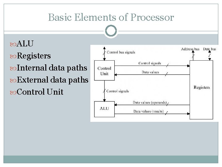
Basic Elements of Processor ALU Registers Internal data paths External data paths Control Unit

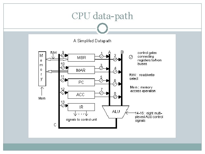
CPU data-path Hardware units like ALU's, registers, memory, etc. , are linked together into a data-path. The flow of bits around the data-path is controlled by the "gates" which allow the bits to flow (on) or not flow (off) through the data-path. The binary instructions (1 = on; 0 = off) that control the flow are called micro-instructions.

CPU data-path

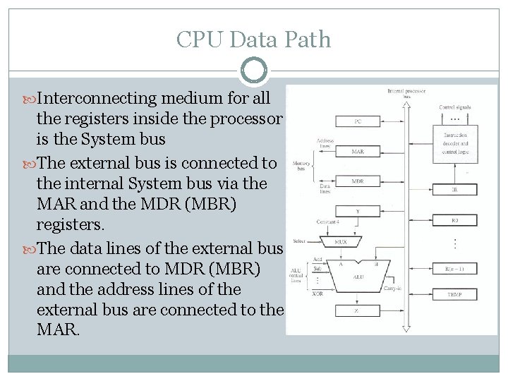
CPU Data Path Interconnecting medium for all the registers inside the processor is the System bus The external bus is connected to the internal System bus via the MAR and the MDR (MBR) registers. The data lines of the external bus are connected to MDR (MBR) and the address lines of the external bus are connected to the MAR.

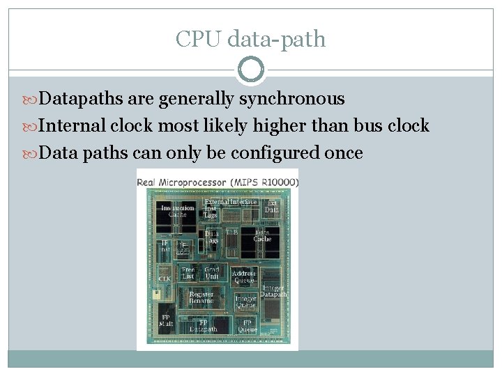
CPU data-path Datapaths are generally synchronous Internal clock most likely higher than bus clock Data paths can only be configured once

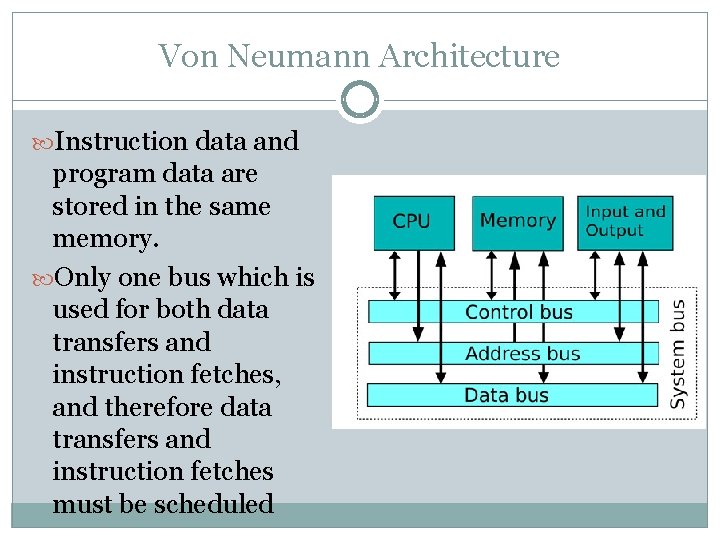
Von Neumann Architecture Instruction data and program data are stored in the same memory. Only one bus which is used for both data transfers and instruction fetches, and therefore data transfers and instruction fetches must be scheduled

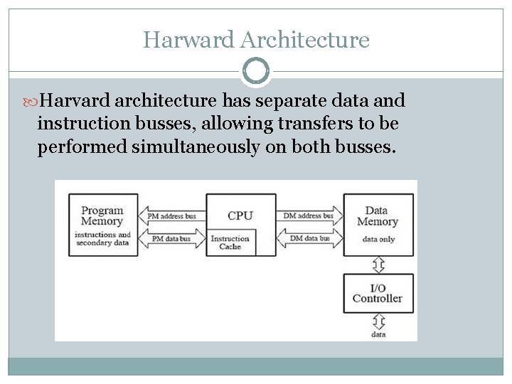
Harward Architecture Harvard architecture has separate data and instruction busses, allowing transfers to be performed simultaneously on both busses.

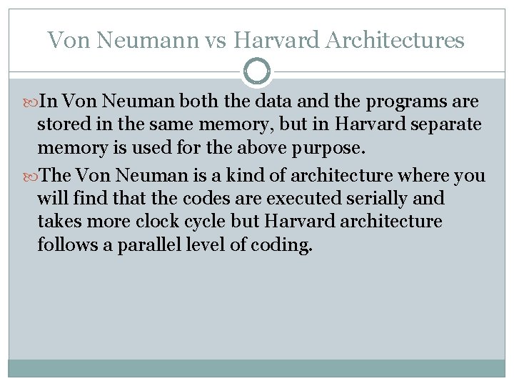
Von Neumann vs Harvard Architectures In Von Neuman both the data and the programs are stored in the same memory, but in Harvard separate memory is used for the above purpose. The Von Neuman is a kind of architecture where you will find that the codes are executed serially and takes more clock cycle but Harvard architecture follows a parallel level of coding.

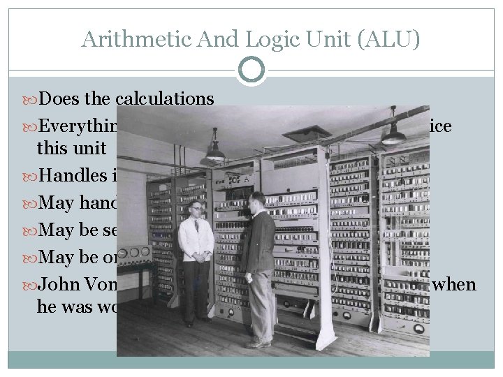
Arithmetic And Logic Unit (ALU) Does the calculations Everything else in the computer is there to service this unit Handles integers May handle floating point (real) numbers May be separate FPU (maths co-processor) May be on chip separate FPU (486 DX +) John Von Neumann proposed the ALU in 1945 when he was working on EDVAC.

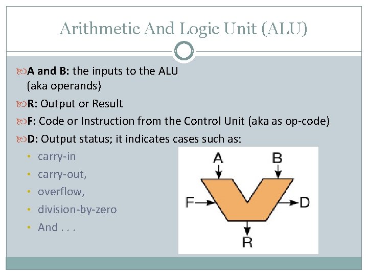
Arithmetic And Logic Unit (ALU) A and B: the inputs to the ALU (aka operands) R: Output or Result F: Code or Instruction from the Control Unit (aka as op-code) D: Output status; it indicates cases such as: • carry-in • carry-out, • overflow, • division-by-zero • And. . .

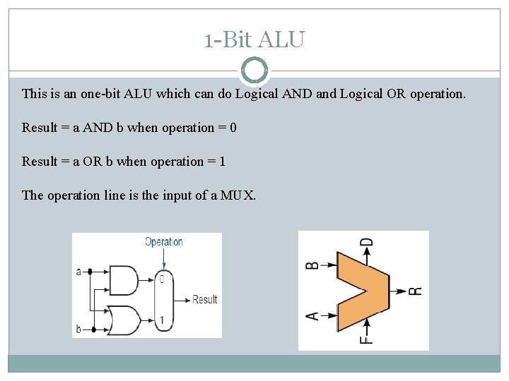
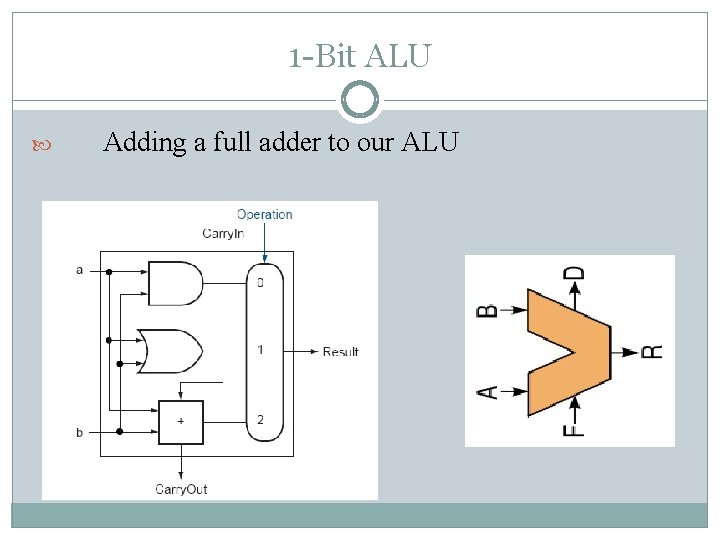
1 -Bit ALU This is an one-bit ALU which can do Logical AND and Logical OR operation. Result = a AND b when operation = 0 Result = a OR b when operation = 1 The operation line is the input of a MUX.

1 -Bit ALU Adding a full adder to our ALU

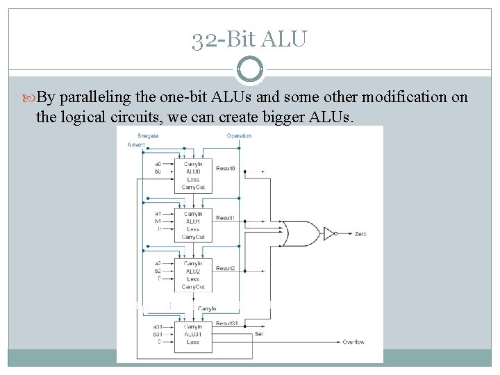
32 -Bit ALU By paralleling the one-bit ALUs and some other modification on the logical circuits, we can create bigger ALUs.

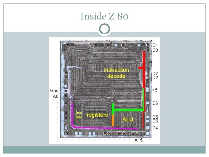
Inside Z 80

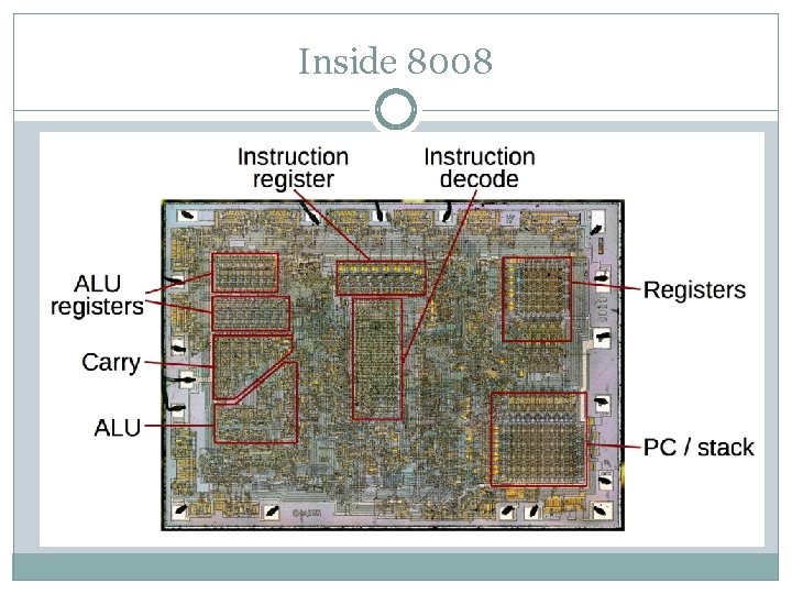
Inside 8008

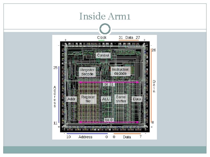
Inside Arm 1

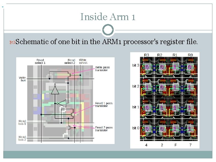
Inside Arm 1 Schematic of one bit in the ARM 1 processor's register file.

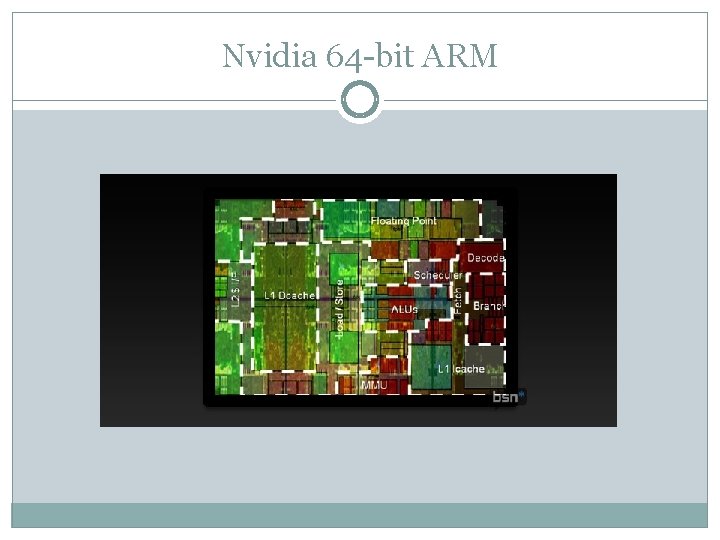
Nvidia 64 -bit ARM

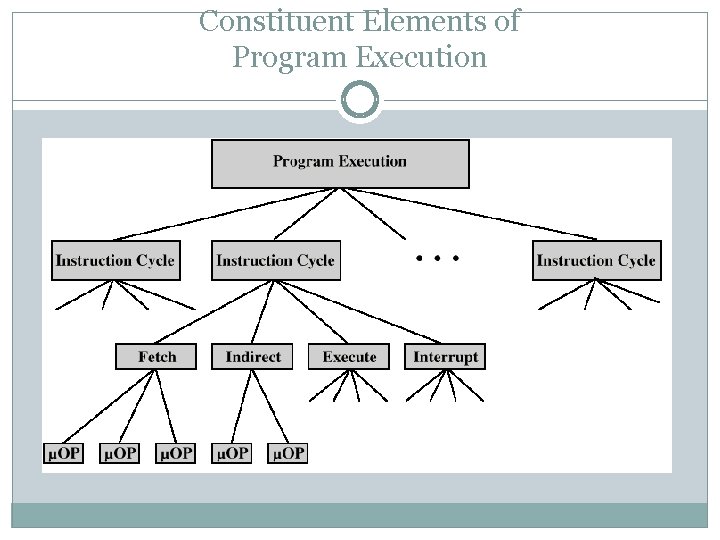
Micro-Operations A computer executes a program Fetch/execute cycle Each cycle has a number of steps called micro- operations Each step does very little atomic operation of CPU

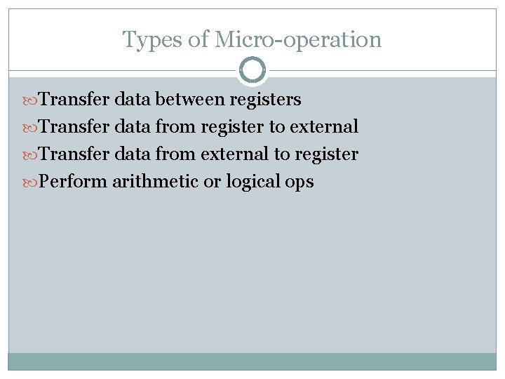
Types of Micro-operation Transfer data between registers Transfer data from register to external Transfer data from external to register Perform arithmetic or logical ops

Constituent Elements of Program Execution

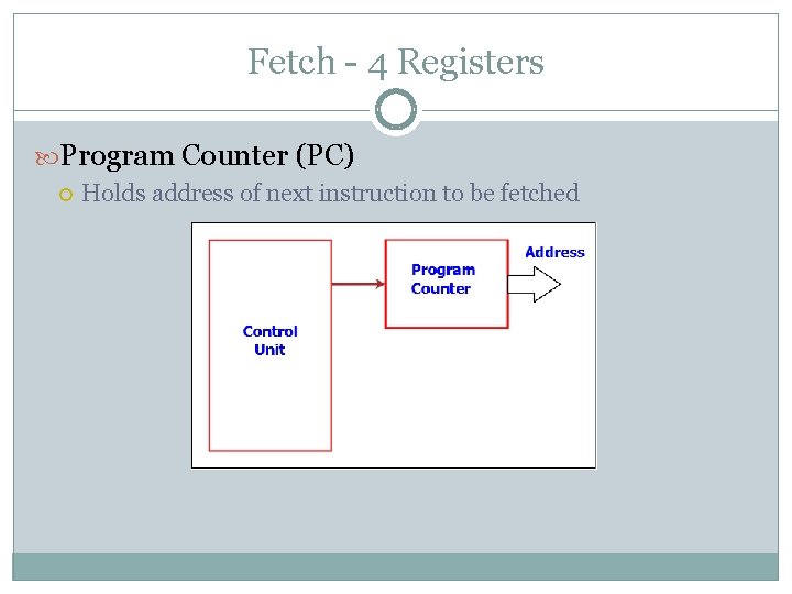
Fetch - 4 Registers Program Counter (PC) Holds address of next instruction to be fetched

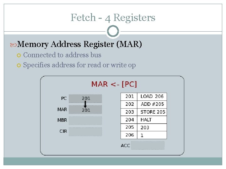
Fetch - 4 Registers Memory Address Register (MAR) Connected to address bus Specifies address for read or write op

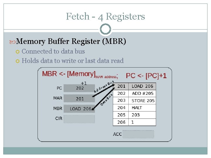
Fetch - 4 Registers Memory Buffer Register (MBR) Connected to data bus Holds data to write or last data read

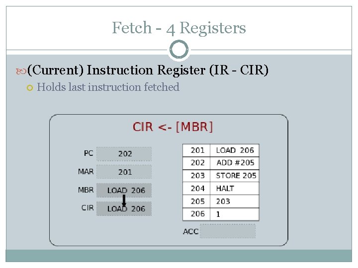
Fetch - 4 Registers (Current) Instruction Register (IR - CIR) Holds last instruction fetched

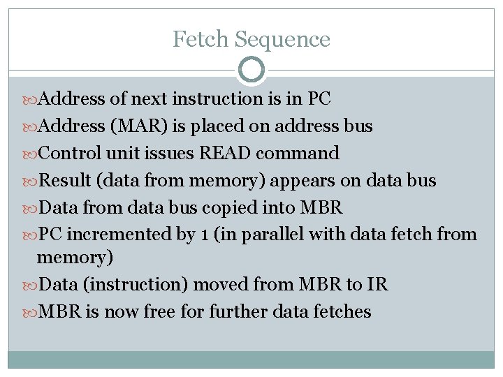
Fetch Sequence Address of next instruction is in PC Address (MAR) is placed on address bus Control unit issues READ command Result (data from memory) appears on data bus Data from data bus copied into MBR PC incremented by 1 (in parallel with data fetch from memory) Data (instruction) moved from MBR to IR MBR is now free for further data fetches

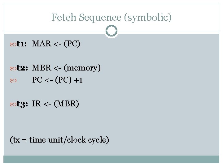
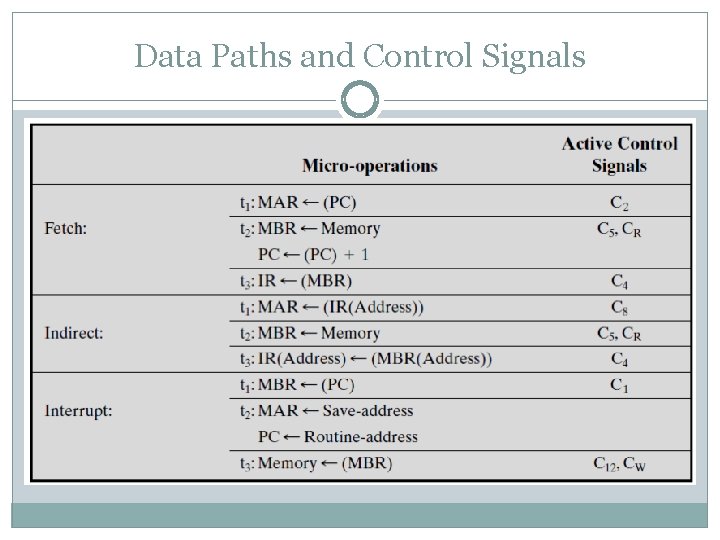
Fetch Sequence (symbolic) t 1: MAR <- (PC) t 2: MBR <- (memory) PC <- (PC) +1 t 3: IR <- (MBR) (tx = time unit/clock cycle)

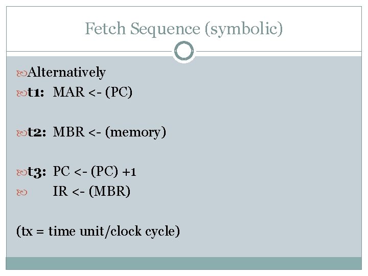
Fetch Sequence (symbolic) Alternatively t 1: MAR <- (PC) t 2: MBR <- (memory) t 3: PC <- (PC) +1 IR <- (MBR) (tx = time unit/clock cycle)

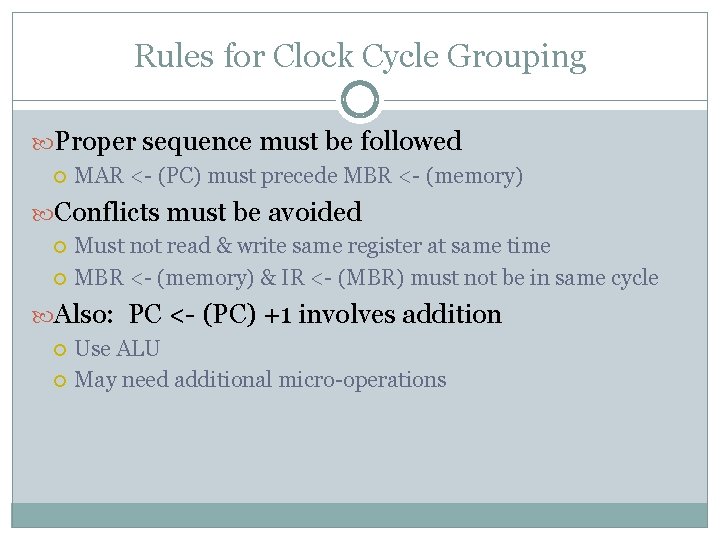
Rules for Clock Cycle Grouping Proper sequence must be followed MAR <- (PC) must precede MBR <- (memory) Conflicts must be avoided Must not read & write same register at same time MBR <- (memory) & IR <- (MBR) must not be in same cycle Also: PC <- (PC) +1 involves addition Use ALU May need additional micro-operations

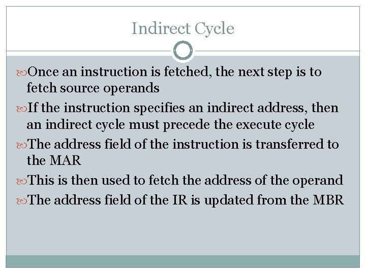
Indirect Cycle Once an instruction is fetched, the next step is to fetch source operands If the instruction specifies an indirect address, then an indirect cycle must precede the execute cycle The address field of the instruction is transferred to the MAR This is then used to fetch the address of the operand The address field of the IR is updated from the MBR

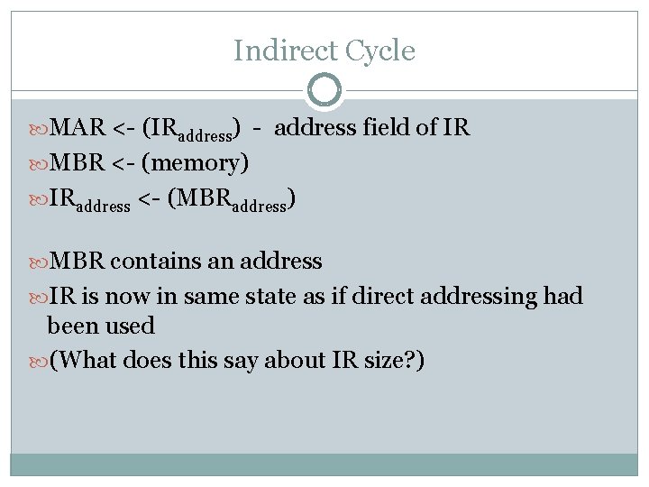
Indirect Cycle MAR <- (IRaddress) - address field of IR MBR <- (memory) IRaddress <- (MBRaddress) MBR contains an address IR is now in same state as if direct addressing had been used (What does this say about IR size? )

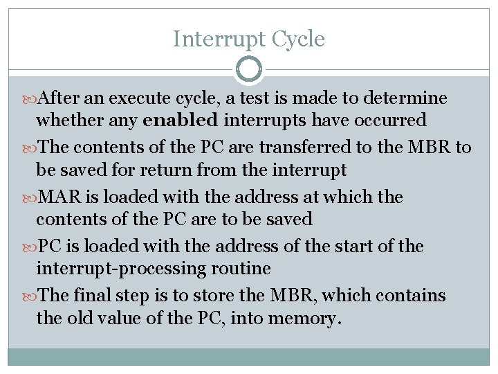
Interrupt Cycle After an execute cycle, a test is made to determine whether any enabled interrupts have occurred The contents of the PC are transferred to the MBR to be saved for return from the interrupt MAR is loaded with the address at which the contents of the PC are to be saved PC is loaded with the address of the start of the interrupt-processing routine The final step is to store the MBR, which contains the old value of the PC, into memory.

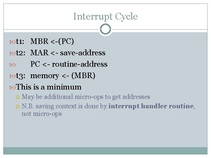
Interrupt Cycle t 1: MBR <-(PC) t 2: MAR <- save-address PC <- routine-address t 3: memory <- (MBR) This is a minimum May be additional micro-ops to get addresses N. B. saving context is done by interrupt handler routine, not micro-ops

Execute Cycle The fetch, indirect, and interrupt cycles are simple and predictable This is not true for the execute cycle There a variety of opcodes, There a number of different sequences of microoperations that can occur

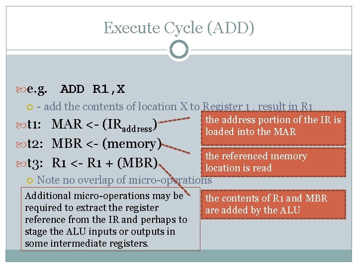
Execute Cycle (ADD) e. g. ADD R 1, X - add the contents of location X to Register 1 , result in R 1 t 1: MAR <- (IRaddress) t 2: MBR <- (memory) t 3: R 1 <- R 1 + (MBR) the address portion of the IR is loaded into the MAR the referenced memory location is read Note no overlap of micro-operations Additional micro-operations may be required to extract the register reference from the IR and perhaps to stage the ALU inputs or outputs in some intermediate registers. the contents of R 1 and MBR are added by the ALU

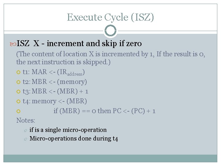
Execute Cycle (ISZ) ISZ X - increment and skip if zero (The content of location X is incremented by 1, If the result is 0, the next instruction is skipped. ) t 1: MAR <- (IRaddress) t 2: MBR <- (memory) t 3: MBR <- (MBR) + 1 t 4: memory <- (MBR) if (MBR) == 0 then PC <- (PC) + 1 Notes: if is a single micro-operation Micro-operations done during t 4

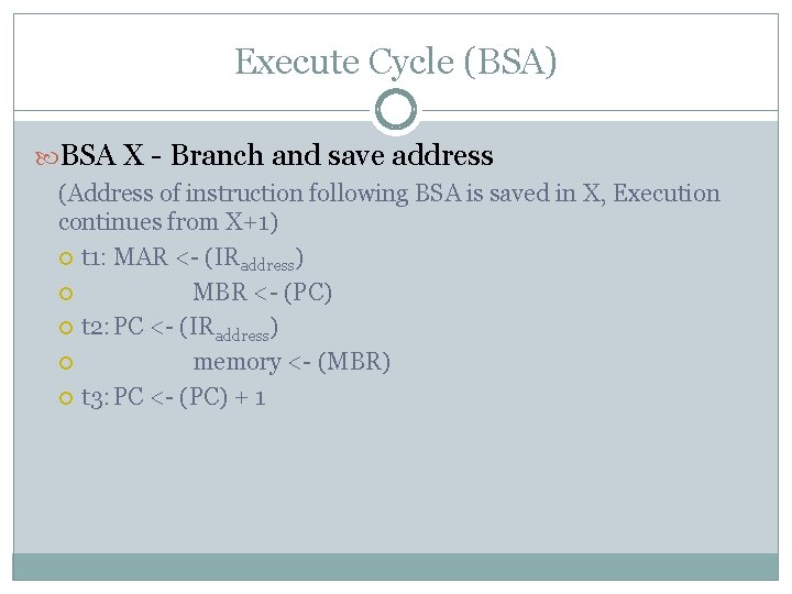
Execute Cycle (BSA) BSA X - Branch and save address (Address of instruction following BSA is saved in X, Execution continues from X+1) t 1: MAR <- (IRaddress) MBR <- (PC) t 2: PC <- (IRaddress) memory <- (MBR) t 3: PC <- (PC) + 1

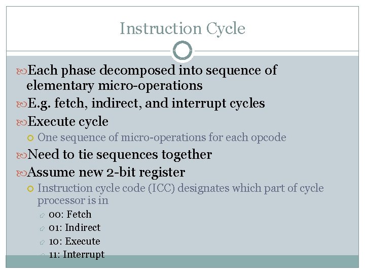
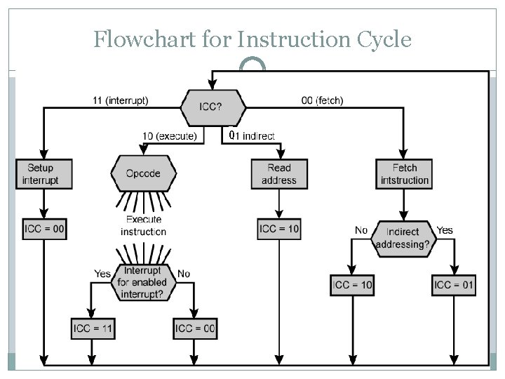
Instruction Cycle Each phase decomposed into sequence of elementary micro-operations E. g. fetch, indirect, and interrupt cycles Execute cycle One sequence of micro-operations for each opcode Need to tie sequences together Assume new 2 -bit register Instruction cycle code (ICC) designates which part of cycle processor is in 00: Fetch 01: Indirect 10: Execute 11: Interrupt

Flowchart for Instruction Cycle 0

Functional Requirements Define basic elements of processor Describe micro-operations processor performs Determine functions control unit must perform

Functions of Control Unit Sequencing Causing the CPU to step through a series of micro-operations Execution Causing the performance of each micro-op This is done using Control Signals

Functions of Control Unit For the control unit to perform its function, it must have inputs that allow it to determine the state of the system outputs that allow it to control the behavior of the system. the control unit must have the logic required to perform its sequencing and execution functions.

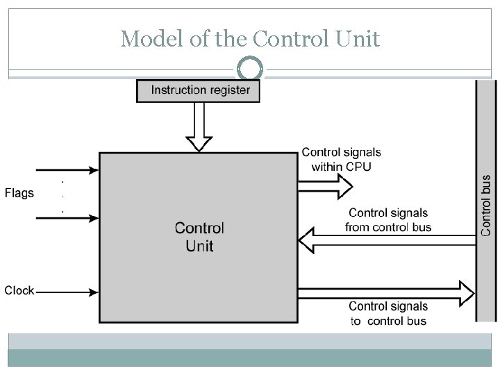
Control Signals Clock One micro-instruction (or set of parallel micro-instructions) per clock cycle referred to as the processor cycle time, or the clock cycle time Instruction register Op-code and addressing mode for current instruction Determines which micro-instructions are performed

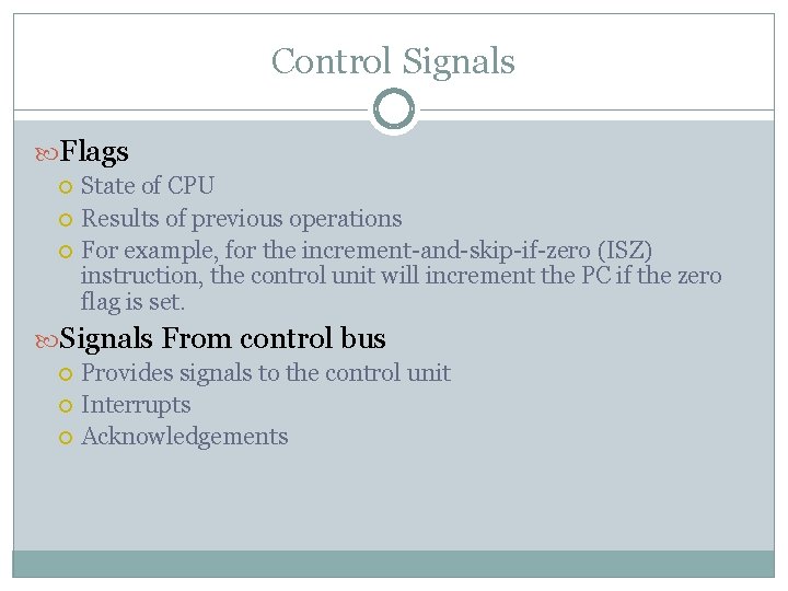
Control Signals Flags State of CPU Results of previous operations For example, for the increment-and-skip-if-zero (ISZ) instruction, the control unit will increment the PC if the zero flag is set. Signals From control bus Provides signals to the control unit Interrupts Acknowledgements

Model of the Control Unit

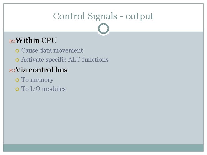
Control Signals - output Within CPU Cause data movement Activate specific ALU functions Via control bus To memory To I/O modules

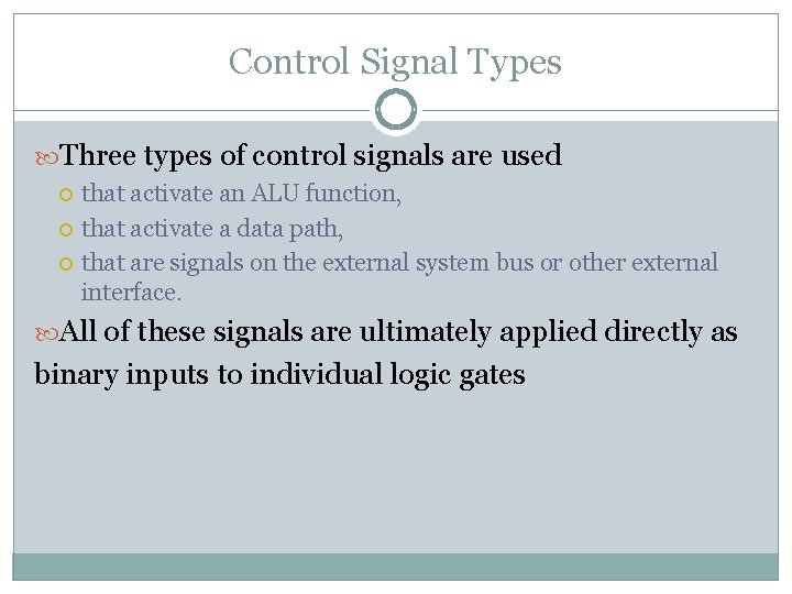
Control Signal Types Three types of control signals are used that activate an ALU function, that activate a data path, that are signals on the external system bus or other external interface. All of these signals are ultimately applied directly as binary inputs to individual logic gates

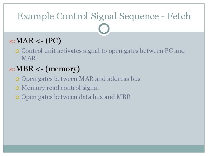
Example Control Signal Sequence - Fetch MAR <- (PC) Control unit activates signal to open gates between PC and MAR MBR <- (memory) Open gates between MAR and address bus Memory read control signal Open gates between data bus and MBR

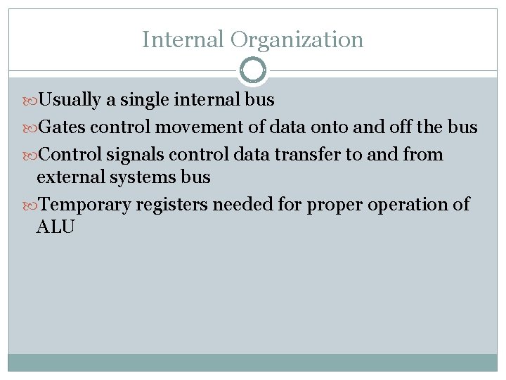
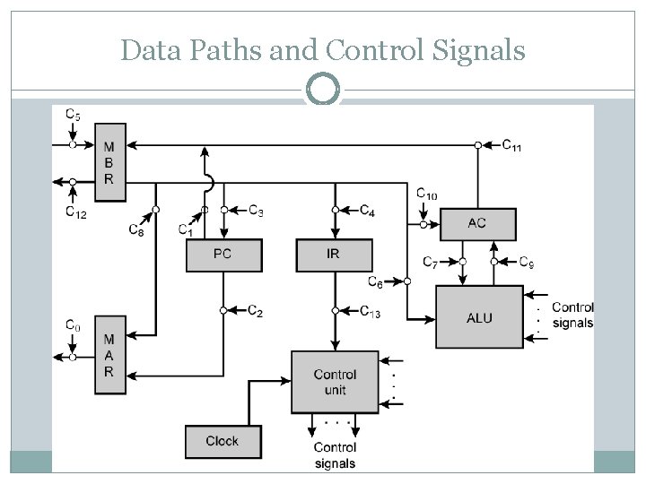
Internal Organization Usually a single internal bus Gates control movement of data onto and off the bus Control signals control data transfer to and from external systems bus Temporary registers needed for properation of ALU

Data Paths and Control Signals

Data Paths and Control Signals

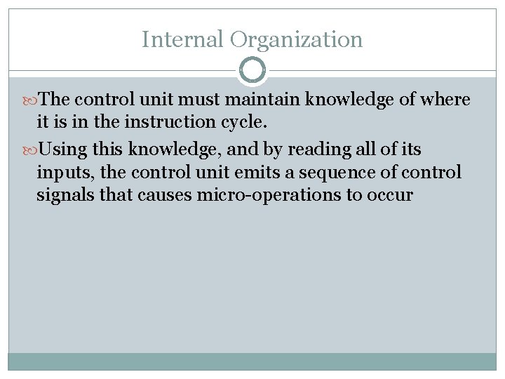
Internal Organization The control unit must maintain knowledge of where it is in the instruction cycle. Using this knowledge, and by reading all of its inputs, the control unit emits a sequence of control signals that causes micro-operations to occur

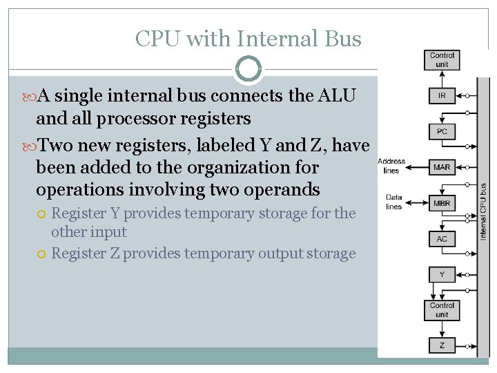
CPU with Internal Bus A single internal bus connects the ALU and all processor registers Two new registers, labeled Y and Z, have been added to the organization for operations involving two operands Register Y provides temporary storage for the other input Register Z provides temporary output storage

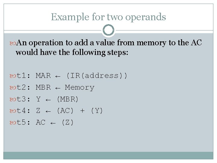
Example for two operands An operation to add a value from memory to the AC would have the following steps: t 1: MAR ← (IR(address)) t 2: MBR ← Memory t 3: Y ← (MBR) t 4: Z ← (AC) + (Y) t 5: AC ← (Z)

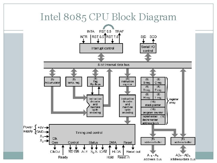
Intel 8085 CPU Block Diagram

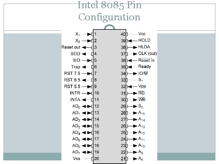
Intel 8085 Pin Configuration

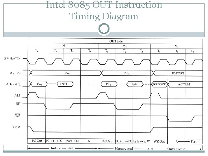
Intel 8085 OUT Instruction Timing Diagram

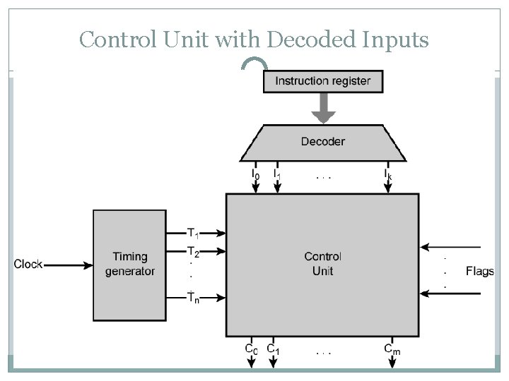
Hardwired Implementation (1) Control unit inputs Flags and control bus Each bit means something Instruction register Op-code causes different control signals for each different instruction Unique logic for each op-code Decoder takes encoded input and produces single output n binary inputs and 2 n outputs

Hardwired Implementation (2) Clock Repetitive sequence of pulses Useful for measuring duration of micro-ops Must be long enough to allow signal propagation Different control signals at different times within instruction cycle Need a counter with different control signals for t 1, t 2 etc.

Control Unit with Decoded Inputs

Problems With Hard Wired Designs Complex sequencing & micro-operation logic Difficult to design and test Inflexible design Difficult to add new instructions

Required Reading Stallings chapter 15