Lecture 3 Combinational Logic Design Chapter 3 Basic

Lecture 3 Combinational Logic Design Chapter 3

Basic Digital Logic Circuits n n We have seen how to implement truth tables and other simple circuits using individual gates. Few circuits are built like this in real world. Instead modules containing many gates are used. We will briefly look at: n n Integrated Circuits Combinational Circuits Arithmetic Circuits Reading: Chapter 3

Integrated Circuits n n Gates are manufactured and sold in units called Integrated Circuits, often called ICs or chips. These are usually either square or rectangular packages of either plastic or ceramic, and have pins to connect them to the outside world. Dual Inline Packages or DIPs have two rows of parallel pins. ICs can be classified according to the number of gates they contain: n n SSI(Small Scale Integrated) circuit: 1 -10 gates MSI(Medium Scale Integrated) circuit: 10 -100 gates LSI(Large Scale Integrated) circuit: 100 -100, 000 gates VLSI(Very Large Scale Integrated) circuit: >100, 000 gates

Integrated Circuits

Combinational Circuits Logic circuits for digital systems may be n combinational : Output is determined by the inputs or n sequential : output is a function of current inputs and previous states.

Combinational Circuits A combinational circuit consists of n Input variables n Output variables n Logic gates and n Interconnections

Design Hierarchy Functional blocks Primitive blocks

Design Hierarchy
 n Reusable (each block")
Design Hierarchy Advantages n Reduce complexity (interconnected 32 NAND gates) n Reusable (each block is designed once)

Design Methods Top Down n Bottom up n

Design Tools n Computer-Aided Design Schematic capture n Libraries of graphic symbols n Logic simulator n Logic synthesizers n n Hardware Description Languages

Analysis Procedure Derivation of Boolean Functions T 1 = B’C T 2 = A’B T 3 = A + T 1 = A + B’C T 4 = T 2 D = (A’B) D = A’BD’ + AD + B’D T 5 = T 2 + D = A’B + D F 1 = A + B’C + BD’ + B’D F 2 = A’B + D

Analysis Procedure Derivation of the Truth Table

Design Procedure n n n From the specifications of the problem determine the number of inputs and outputs Derive the truth table that defines the relations between the inputs and the outputs. Obtain the simplified Boolean function for each output Draw the logic diagram Verify the correctness of the design

Example 3 -1 Design of a Combinational Circuit n Design a combinational circuit with three inputs, and one output. The output must be logic 1 when the inputs is less than 3 (011). Use only NAND gates

Code Converters
")
Code Converters W = A + BC+ BD = A + B(C + D) X = B’C + B’D + BC’D’ = B’(C + D) + BC’D’ Y = CD + C’D’ = (C D)’ Z = D’

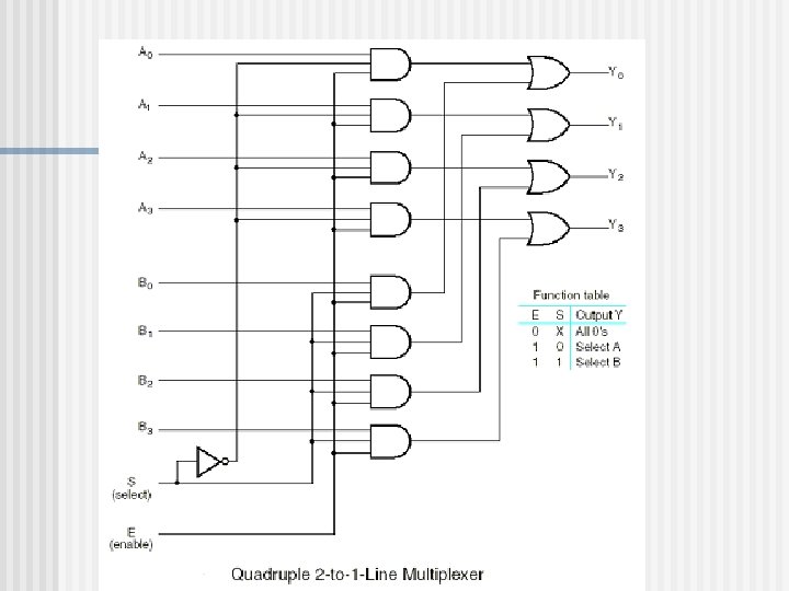
Multiplexers n n n A multiplexer is a circuit with 2 n data inputs, one data input and n control inputs that select one of the outputs. The selected data input is selected “gated” (routed) to the output. The n inputs encode an n-bit number that specifies which input is selected as the output.

E X A M P L E With power and ground added it can be packed in a 14 -pin package.

A Multiplexer Application

Example: Use 4: 1 MUX and apply XY as selecting variables and Z as input for a given function F. F(X, Y, Z) = (1, 2, 6, 7)

A Multiplexer Application Multiplexers can be used in parallel to serial conversion. n Put 8 -bits of data on the input lines. n Step the control lines sequentially from 000 - 111 n

Demultiplexers The inverse of a multiplexer is a demultiplexer. n Single input signal is routed to one of output signals through the selection of control lines. n

Demultiplexers

Decoders n A decoder is a circuit which takes an n-bit number as input and uses it to n select (set to 1) exactly one of its 2 outputs.

E X A M P L E
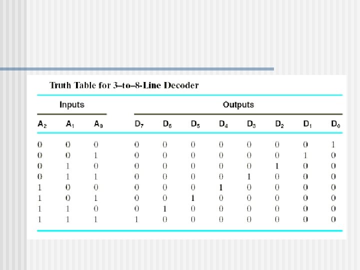

2 -4 Line Decoder

Decoder Expansion

Example: Implement a full-adder circuit with a decoder and OR gates. S (X, Y, Z) = (1, 2, 4, 7) C (X, Y, Z) = ( 3, 5, 6, 7)

Encoders n An encoder is a digital function that performs the inverse operation of a decoder.

Priority Encoder

Adders A hardware circuit for performing addition is an essential part of every CPU. Below is a truth-table for 1 -bit addition along with a circuit known as the half-adder. There are two outputs present: the sum of the inputs, A and B, and the carry to the next(leftward) position.

The Full Adder A half-adder is adequate for summing the low-order bits of two multi-bit input words, but it will not to do for a bit position in the middle of the word because it does not handle the carry into the position from the right. We need a full adder. The truth table and circuit for the full adder will be given next.

The Full Adder

How does the Full Adder Work? From inspection, a full adder is built up from two half adders. The Sum output line is 1 if an odd number of A, B and the Carry in are 1. The Carry out is 1 if either A and B are both 1 (left input to the OR gate) or exactly one of them is 1 and the Carry in bit is also 1. Together the half adders generate both the sum and carry bits.

Binary Ripple Carry Adder

Binary Adder Subtractor

Overflow

Binary Multipliers

A 4 -bit by 3 -bit Binary Multiplier

Decimal Arithmetic Sum can be at most 19=9+9+1 Sum Binary 10 11 12 13 14 15 16 1 1010 1011 1100 1101 1110 1111 0000 17 1 18 1 19 1 0001 0010 0011 C = K + Z 1 Z 3 + Z 2 Z 3
- Slides: 43